Au@Cu2O core–shell nanoparticles as chemiresistors for gas sensor applications: effect of potential barrier modulation on the sensing performance†
Prabhakar
Rai
a,
Rizwan
Khan
a,
Sudarsan
Raj
a,
Sanjit Manohar
Majhi
a,
Kyung-Kuen
Park
a,
Yeon-Tae
Yu
*a,
In-Hwan
Lee
a and
Praveen Kumar
Sekhar
b
aDivision of Advanced Materials Engineering and Research Centre for Advanced Materials Development, College of Engineering, Chonbuk National University, Jeonju 561-756, South Korea. E-mail: yeontae@jbnu.ac.kr; Fax: +82-63-270-2305; Tel: +82-63-270-2288
bNanomaterials and Sensor Laboratory, School of Engineering and Computer Science, Washington State University Vancouver, 14204 NE Salmon Creek Avenue, Vancouver, WA 98686, USA
First published on 14th October 2013
Abstract
Au@Cu2O core–shell nanoparticles (NPs) were synthesized by a solution method at room temperature and applied for gas sensor applications. Transmission electron microscopy (TEM) images showed the formation of Au@Cu2O core–shell NPs, where 12–15 nm Au NPs were covered with 60–30 nm Cu2O shell layers. The surface plasmon resonance (SPR) peak of Au NPs was red-shifted (520–598 nm) after Cu2O shell formation. The response of Au@Cu2O core–shell NPs was higher than that of bare Cu2O NPs to CO at different temperatures and concentrations. Similarly, the response of Au@Cu2O core–shell NPs was higher than that of bare Cu2O NPs for NO2 gas at low temperature. The improved performance of Au@Cu2O core–shell NPs was attributed to the pronounced electronic sensitization, high thermal stability and low screening effect of Au NPs.
Introduction
Heterostructured nanomaterials with chemically distinct components induced by heterointerfaces have led to new applications in the field of catalysis, photovoltaic devices, sensors, and so on.1–3 Recently, enormous efforts have been devoted to fabricating heterostructured materials, heterojunction nanowires and arrays.4–6 Heterojunction nanomaterials with multi-layer structures (which have multi-barrier structures) lead to accumulation of carriers and control of their transport properties which play an important role in modern device physics and have various important applications.7,8 Also, much attention has been focused on creating high performance gas sensors in recent decades, due to the growing awareness about environmental pollution and safety issues. Among various gas sensors, metal oxide semiconductors (MOS) are commercially used for gas monitoring. Resistance changes in metal oxide based gas sensors are used extensively to monitor toxic gases, including CO, hydrocarbons, NOx and hydrogen.9–16 Many metal oxide gas sensors do not exhibit gas sensitivity at room temperature. As a result, gas sensors often require a heating device to achieve the sensitivity. Unfortunately, the high temperature is harmful and is a drawback to the durability of sensors and their performances.17 It is well known that the performance of gas sensors is gauged by their sensitivity, selectivity, response, recovery time, stability, and reproducibility.18–20 Rapid response characteristics with adequate sensitivity, in particular, are required for real-time monitoring of toxic gases and preventing possible disasters from such harmful gases. To meet the issue, it is very important to make efforts in the design and engineering of novel materials to achieve the desired performance. There have been efforts to solve the sensor operating temperature limitation21via nanostructured materials with ultra-high surface-to-volume ratios, element doping, and surface modification with noble metals.22–25 However, noble metal NPs are not stable against heating, which results in a loss of catalytic activity, a serious issue in many applications including gas sensors. The catalytic activity loss is caused by the increased mobility of the metal NPs on the support at higher temperatures.26 It results in either a shunting layer or an active membrane filter effectively obstructing the penetration of the targeting gas into the surface of the gas sensing matrix. In addition, noble metal NPs can be poisoned by many chemicals that contain sulfur (H2S, SO2, and thiols) or phosphorus.27 Nevertheless, the production of gas sensors operating at room temperature with high sensitivity and selectivity with low power consumption remains a challenging task. Therefore, the developments of new sensors to overcome such issues are required.Heterostructures with metal cores and semiconductor shells become the strongest candidates as gas sensors due to their controllable chemical and thermal stabilities within the shell and charge transfer between metal core and semiconductor shells.28–30 Recently, in our lab, the same strategy was applied to Au@SnO2 core–shell nanostructures, which enhanced the sensitivity to CO gas as compared to bare SnO2 at low operating temperature.28 Also, a similar strategy was used in Au@TiO2 core–shell nanostructures for high temperature CO sensing.29 The improved response in metal/n-type MOS is mainly explained by the increase in depletion layer formation due to chemical as well as electronic sensitization of noble metals. Since the response (Rs) of n-type MOS is examined either by Ra/Rg or (Ra − Rg)/Ra for reducing gases, the high Ra value for metal/metal oxide improves the response. Although, the response increases with metal NPs in n-type MOS, the high baseline resistance results in an increase in power consumption for their practical applications. However, such a problem or drawback can be solved using p-type MOS. The transfer of electrons from p-type MOS to metal NPs will increase the hole mobility, thereby decreasing their resistance. Furthermore, in p-type MOS, the response (Rs) is measured either by Rg/Ra or (Rg − Ra)/Ra for reducing gases, and therefore the low Ra value for metal/p-type MOS improves the response.
Among various metal oxides, cuprous oxide (Cu2O), an important p-type semiconducting material with a unique optical and electrical property, is an appealing candidate for solar energy conversion, sensors, photo-catalytic degradation, and coherent propagation of excitons.31–34 The p-type Cu2O has been widely chosen as a sensing material in recent years.35 In this work, Au@Cu2O core–shell NPs have been synthesized and used for the detection of CO and NO2 gases at various temperatures and concentrations and their sensing mechanisms are discussed in detail. The use of Au@Cu2O core–shell NPs towards CO and NO2 gas detection has not been reported before to our knowledge. Also, the advantage of Au@Cu2O core–shell NPs over bare Cu2O NPs is examined and the possible role of Au NPs in sensing mechanisms is discussed. The results demonstrate that Au@Cu2O core–shell NPs are better sensing materials as compared to bare Cu2O NPs.
Experimental
Material synthesis
The Au NPs and Au@Cu2O core–shell NPs were synthesized by using a simple solution process reported elsewhere.28,36 In brief, for synthesis of Au NPs, HAuCl4 solution (250 mL, 1 mM) was heated with mild stirring until boiling. A solution of tri-sodium citrate (25 mL, 34 mM) was then added to the solution with rapid stirring. The resulting solution was kept at 97 °C for 15 min with constant stirring. The resulting solution was finally allowed to cool down at room temperature.For the synthesis of Au@Cu2O core–shell NPs, 1.0 g of PVP was dissolved in 50 mL of 0.01 M Cu(NO3)2 aqueous solution under constant magnetic stirring and the solution was kept for 10 min to dissolve the PVP completely. Afterwards, 1 mL of fresh prepared Au colloid solution was added, followed by the immediate introduction of 20 μL of N2H4·3H2O solution (80 wt%, Sigma-Aldrich) into the reaction mixture. After completion of the reaction, Au@Cu2O core–shell NPs were washed with water and anhydrous ethanol and re-dispersed in ethanol and finally stored in a refrigerator at 4 °C for further investigation. Bare Cu2O NPs were also synthesized by a similar method without Au NPs.
Material characterization
The transmission electron microscopy (TEM) images and high-resolution TEM (HRTEM) images were taken with a JEM-2010 JEOL instrument with a tungsten filament, using an accelerating voltage of 200 kV. The crystallographic structures of the solid samples were determined with a D/Max 2005 Rigaku X-ray diffractometer equipped with graphite monochromatized high-intensity Cu Kα radiation (λ = 1.54187 Å). The UV-visible spectra were recorded on a UV-visible spectrometer (UV-2550, Shimadzu).Gas sensing measurements
The gas sensors were fabricated with the as-synthesized Au@Cu2O core–shell NPs as sensing materials. To measure the sensor response of the Au@Cu2O core–shell NPs for CO and NO2 gases, a sensor device was prepared as follows;28 the synthesized Au@Cu2O colloid was dropped onto the cleaned Al2O3 board (15 mm × 15 mm) with interdigitated platinum electrodes (10 mm × 10 mm) and the colloid was dried on a hot plate. The Au@Cu2O core–shell NPs loaded device was heated treated at 300 °C in a muffle furnace for 5 h. The change in resistance of the device due to the presence of CO and NO2 gases was measured using a high resistance meter (Agilent 34970A). The device was examined in the temperature range of 25–250 °C at various concentrations of CO (100–1000 ppm) and NO2 (5–100 ppm) in a temperature-controlled environment. The background gas was N2, and the dry air was mixed with 10.5% of oxygen. The gas flow rate (100 cm3 min−1) over the sensor device was switched between the sample gas and dry air to record the sensor response to electrical resistance.The sensor response (Rs) was calculated using Rg/Ra for CO gas and Ra/Rg for NO2 gas. Here, Ra is the resistance in dry air and Rg is the resistance in the probe gas.
Results and discussion
Fig. 1 displays the formation of Au@Cu2O core–shell NPs with Au NPs as a core and Cu2O as a shell. The Au NPs are well dispersed, spherical in shape and their size ranges from 12–15 nm as shown in Fig. 1a. The formation of heterogeneous Au@Cu2O core–shell NPs is shown in Fig. 1b and c. The overall size of Au@Cu2O core–shell NPs is 120–80 nm, where the size of the Au NP cores is about 12–15 nm and the Cu2O shell thickness is about 60–30 nm. It was apparent from the image that each core–shell NP only contained a single Au NP core. In order to obtain more detailed growth information on the shell formation of the Au@Cu2O core–shell NPs, HRTEM was applied and the results are shown in Fig. 1d. The local crystalline lattices at the hetero-interface of the Au and Cu2O shells revealed that the well-defined interface and continuity between metallic Au NPs and Cu2O shells are indicative of the strong interaction between exposed Au and Cu2O crystals.36 However, without Au NPs, solid spherical shaped Cu2O NPs are formed with size ranges from 150–200 nm (see Fig. S1 in the ESI†). X-ray diffraction (XRD) patterns of Au@Cu2O core–shell NPs exhibit that the Cu2O shells (JCPDS no. 03-065-3288) have formed on the surface of the face-centered-cubic (fcc) metallic Au nanocrystals (JCPDS no. 98-000-0230) without amorphous or additional phases (see Fig. S2 in the ESI†). The XRD peaks from Cu2O were significantly broadened largely due to the small size of the primary Cu2O nanocrystallites in the shells. | ||
| Fig. 1 TEM images of Au NPs (a), Au@Cu2O core–shell NPs (b and c) and HRTEM of the selected area of single Au@Cu2O core–shell NPs (d). | ||
The formation of Au@Cu2O core–shell NPs is further characterized by UV-visible spectroscopy. The SPR peaks of the Au NPs is red-shifted in Au@Cu2O core–shell nanostructures, caused by the larger refractive index of Cu2O encapsulating the Au cores.36 As shown in Fig. 2, the Au NP absorption peak is recorded at 520 nm, which is red-shifted to 598 nm after Cu2O shell formation. The weak SPR response is attributed to the thick Cu2O shells for individual core–shell Au@Cu2O NPs. The Cu2O characteristic absorption peak for Au@Cu2O core–shell NPs is recorded at 458 nm.
 | ||
| Fig. 2 UV-visible spectra of Au and Au@Cu2O core–shell NPs. | ||
To demonstrate the potential application of the as-prepared Au@Cu2O core–shell NPs in a gas sensor, we examined the detection of CO and NO2 gases based on the present Au@Cu2O core–shell NPs. Also, the advantage of using Au NPs in Au@Cu2O core–shell NPs is examined by comparing their response with that of bare Cu2O NPs. Fig. 3 presents the sensing performance toward CO based on the two types of Cu2O spheres, that is, Au@Cu2O core–shell NPs and Cu2O NPs. It shows that the resistance increases after the introduction of CO gas and reaches a saturation stage. When the supply of CO gas is stopped, the resistance starts to decrease again and returns to its original value. This typically shows the p-type semiconducting behavior. It can be seen that the baseline resistance of Au@Cu2O core–shell NPs is very low as compared to Cu2O NPs. The sensitivity of metal oxides depends on the extent of adsorption and desorption, whereas the response and recovery time depend on the speed of adsorption and desorption processes. Therefore, Au@Cu2O core–shell NPs show better sensing capability than bare Cu2O NPs. The response of Au@Cu2O core–shell NPs is higher than that of Cu2O NPs. For example, the response of Cu2O and Au@Cu2O core–shell NPs for 1000 ppm of CO gas is 3.35 and 5.67, respectively. For both devices, the response increases with increasing gas concentration. Furthermore, reproducibility is also an important factor, which is checked by repeating the response for 1000 ppm three times. It can be seen from Fig. 3 that Au@Cu2O core–shell NPs exhibit better reproducibility than bare Cu2O NPs. The value for response and recovery times is also measured. For example the response time (T90%) for Au@Cu2O core–shell and bare Cu2O NPs is calculated as 3.37 and 5.12 min, respectively, for 1000 ppm of CO gas from Fig. 3. Similarly, the recovery time (T90%) of Au@Cu2O core–shell NPs is calculated as 6.45 min from Fig. 3, whereas bare Cu2O has a very long recovery time. The values indicate that the response and recovery times of Au@Cu2O core–shell NPs are better than those of bare Cu2O NPs. Thus, the sensor fabricated from Au@Cu2O core–shell NPs exhibits a detection limit of 100 ppm, a broader dynamic linear range from 100 to 1000 ppm, higher sensitivity, shorter response time, and recovery time for CO sensing, compared with those obtained by bare Cu2O NPs.
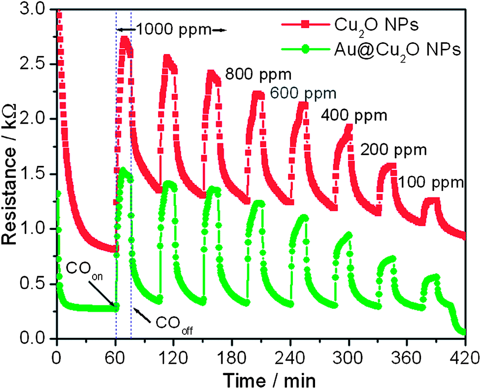 | ||
| Fig. 3 Changes in electrical resistance toward different concentrations of CO at a working temperature of 200 °C obtained at bare Cu2O and Au@Cu2O core–shell NPs. | ||
The effect of testing temperature on the sensing behavior of both devices is also examined and illustrated in Fig. 4. It can be seen that the response increased with increasing temperature for bare Cu2O NPs. However, for Au@Cu2O core–shell NPs the response increases up to 200 °C and then slightly decreased at 250 °C. Au@Cu2O core–shell NPs show the maximum response of 5.67 at 200 °C, whereas bare Cu2O shows a response of 4.35 at 250 °C for 1000 ppm of CO gas. Meanwhile, no response curve is observed for bare Cu2O NPs below 200 °C, whereas Au@Cu2O core–shell NPs show a 3.09 response at 150 °C for 1000 ppm of CO gas. Furthermore, the sensitivity (slope between ‘Rg/Ra’ and ‘concentration’) of these two samples can be compared by comparing the slope of a calibration graph in Fig. 4a and b. The sensor having an Au@Cu2O core–shell layer exhibits a higher sensitivity and better dynamics behavior towards CO than that with bare Cu2O NP layers. Thus, the above results demonstrate that the introduction of Au NPs as a core in the Cu2O system improves its sensing performance in terms of sensitivity, response time, recovery time and lower operating temperature.
 | ||
| Fig. 4 Plot of response versus CO concentration, and working temperature obtained at (a) Au@Cu2O core–shell NPs and (b) bare Cu2O NPs. | ||
Also, the sensing properties of both devices are examined for oxidizing gas, such as NO2, to investigate the role of Au NPs on the sensing performance of Cu2O NPs. The dynamic response of bare Cu2O and Au@Cu2O core–shell NP sensors for room temperature detection with increasing concentration of NO2 gas (5–100 ppm) is displayed in Fig. 5a. The plot reveals that the resistance decreases after the introduction of NO2 gas and reaches saturation. Once the NO2 feed is stopped, the resistance begins to increase again and returns to its original value. Interestingly, the baseline resistance of Au@Cu2O core–shell NPs is very high as compared to that of bare Cu2O NPs. During the exposure of NO2 the response of both devices increases with increasing gas concentration. The maximum response is 3.23 for Au@Cu2O core–shell NPs, whereas it is 1.28 for bare Cu2O NPs for 100 ppm of NO2 gas. This is the first demonstration of NO2 gas sensing by Au@Cu2O core–shell NPs to our knowledge, where a low detection limit has been achieved at room temperature. Previously, Deng et al. studied on NO/NO2 sensing by Cu2O nanostructures and found room temperature sensitivity after addition of reduced graphene.37
 | ||
| Fig. 5 Changes in electrical resistance of bare Cu2O NPs and Au@Cu2O core–shell NPs toward different concentrations of NO2 at (a) room temperature and (b) 250 °C. | ||
In addition, the temperature dependent sensing property is investigated for core–shell NPs. The baseline resistance of Au@Cu2O core–shell NPs is very high as compared to that of bare Cu2O NPs at low temperatures and decreases with increasing temperature as shown in Fig. 5 (also see the ESI, Fig. S3†). Finally, the baseline resistance of Au@Cu2O core–shell NPs becomes lower than that of bare Cu2O NPs above 50 °C. Although, the baseline resistance decreases for both devices but the decrease for Au@Cu2O core–shell NPs is much sharper. More interestingly, the response curve is opposite for both devices at 250 °C as displayed in Fig. 5b. The responses of these devices are plotted against gas concentration at different temperatures and are presented in Fig. 6. The sensitivity of these two samples can be compared by comparing the slope of a calibration graph in Fig. 6a and b. The sensor having Au@Cu2O core–shell layers exhibits a higher sensitivity to NO2 than that with bare Cu2O NP layers at low operating temperatures. It can be seen that the response decreases with increasing temperature for Au@Cu2O core–shell NPs, whereas the sensor response increases for bare Cu2O NPs. For example, the response decreases from 3.23 to 1.47 at 25 °C to 250 °C for Au@Cu2O core–shell NPs. Also, it did not show any response at 200 °C. Meanwhile, the response at 150 °C is slightly higher than that at 250 °C, but the response curve is not stable, and therefore it could be ignored (see the ESI, Fig. S3†). However, the response of Cu2O NPs increases from 1.28 to 2.14 for 100 ppm of NO2 gas, when the temperature is increased from 25 °C to 200 °C. In addition, when the temperature reaches above 200 °C the response slightly decreases to 1.75. However, the response of Au@Cu2O core–shell NPs is higher than that of bare Cu2O NPs below 200 °C and lower above 150 °C at every concentration of NO2 gas. Meanwhile, the difference in the response curve of both devices suggests that they behave like p-type semiconductors below 200 °C and n-type semiconductors above 200 °C for NO2 gas.
 | ||
| Fig. 6 Plot of response versus NO2 concentration, and the working temperature obtained at (a) Au@Cu2O core–shell NPs and (b) bare Cu2O NPs. | ||
The operating principles of p-type transition metal oxide gas sensors are based on the change of sensor conductivity by controlling mobile charge carriers. When the Cu2O sensor is exposed to air, oxygen molecules adsorb on the surface of the materials to form O2−, O−, and O2− ions by capturing electrons from the conduction band. The transfer of electrons to oxygen species generates holes, and therefore the resistance decreases.
When the Cu2O sensor is exposed to CO environments, the adsorbed CO gas then reacts with the chemisorbed oxygen anions at the surface; the reaction can be described as follows:
| 2CO(gas) + 2O−(ads) → 2CO2(gas) + 2e− | (1) |
The gas removes chemisorbed oxygen anions and is oxidized. The electrons from the red–ox reactions between CO and adsorbed surface oxygen are injected into the conduction band of Cu2O, and the recombination between the electrons and holes results in a lower carrier concentration. Subsequently, the resistance of Cu2O increases. The significant variation in resistance can be attributed to the special structural advantages of the Au@Cu2O core–shell NPs. The low baseline resistance of Au@Cu2O compared to that of bare Cu2O NPs can be explained on the basis of electronic and chemical sensitization of Au NPs.10,28 The electronic sensitization of Au NPs results in the transfer of electrons from the conduction band of Cu2O to Au NPs, because the Au work function (5.1 eV) is larger than that of Cu2O (4.84 eV). Thus, the energy band bends higher at the Au–Cu2O interface, which results in greater electron withdrawal and the increase in hole mobility.38 In chemical mechanisms, Au NPs catalytically activate the dissociation of molecular oxygen, whose atomic products then adsorb onto the Cu2O support resulting in a greater degree of electron withdrawal from the Cu2O than for the bare Cu2O, which again results in the increase in hole mobility. Therefore, the resistance of Cu2O decreases with the introduction of Au NPs. A schematic illustration of charge transfer in the Au–Cu2O system is shown in Fig. 7. Since the response is measured by Rg/Ra for CO gas, the lowering of the Ra for Au@Cu2O core–shell NPs results in an increase in response.
 | ||
| Fig. 7 Energy band diagram and conduction of current in Au@Cu2O core–shell NPs. | ||
On the other hand, when the Cu2O sensors are exposed to NO2 gas, which is a better oxidizing agent than oxygen, it adsorbs directly on the surface of Cu2O NPs.39
| NO2(gas) + e− → NO2−(ads) | (2) |
The above reactions result in the decrease in concentration of electrons on the surface of Cu2O and promotes the hole conductivity in the Cu2O device, which results in a decrease in resistance of the material. This change in resistivity can be used for the detection of NO2. However, this phenomenon occurs only at low temperatures (below 200 °C) while at high temperatures (250 °C) the response transient is opposite and behaves like an n-type semiconductor. This change in response transient can not be explained on the basis of transition of p-type Cu2O NPs to n-type because the same sample shows a typical p-type semiconductor sensing property for CO gas at these temperatures. Therefore, this change in response transient is possibly related to the NO2 gas chemistry. It is well known that above 150 °C, NO2 decomposes with the release of oxygen via an endothermic process.40
| 2NO2(g) → 2NO(g) + O2(g) | (3) |
In the case of NO, it reacts with adsorbed oxygen species and forms NO2 gas.41
| NO(g) + O2−(ads) → NO2(g) + 2e− | (4) |
The electrons from the red–ox reactions between NO and adsorbed surface oxygen are injected into the conduction band of Cu2O, and the recombination between the electrons and holes results in a lower carrier concentration. Subsequently, the resistance of Cu2O increases. However, still more work is needed to completely understand such behaviors.
Again, the response of Au@Cu2O is higher than bare Cu2O NPs at low temperature and it can be explained on the basis of baseline resistance. For example, at room temperature, the sensor shows a typical p-type semiconductor sensing behavior and the response is measured by Ra/Rg. Since Ra of Au@Cu2O is higher than bare Cu2O NPs, its response is also higher. A further increase in temperature leads to a decrease in response for Au@Cu2O, whereas an increase in bare Cu2O as shown in Fig. 8a. However, the response of Au@Cu2O is higher than that of bare Cu2O NPs up to 100 °C. From 150 °C to 250 °C, the response transients are not stable, therefore it is difficult to distinguish which sensor device has better sensing performance (see the ESI, Fig. S3†). Again above 200 °C the response transient of Au@Cu2O is better than bare Cu2O NPs. Furthermore, it can be seen from Fig. 8b that the baseline resistance decreases with an increase in temperature, but this decrease in Au@Cu2O is very sharp and possibly this is the reason why the response decreases with increasing temperature.
 | ||
| Fig. 8 Temperature dependent (a) response for 100 ppm NO2 gas and (b) baseline resistance of bare Cu2O and Au@Cu2O core–shell NPs. | ||
The decrease in baseline resistance with temperatures is interesting and needs to be explained. The baseline resistance depends on the height of the potential energy barrier to carrier transport between neighboring grains in the metal oxide, which is a function of temperature. It is examined by the manner in which carrier transport occurs. In metal oxide sensors, the carrier migrates from one grain to another, which is a temperature-dependent property.42 If we consider a migration transport path with resistance Rm, then Rm increases exponentially according to eqn (5)
Rm = Rmo![[thin space (1/6-em)]](https://www.rsc.org/images/entities/char_2009.gif) exp(eVs/RT) exp(eVs/RT) | (5) |
Apart from temperature, the potential energy barrier is also a function of atmosphere oxygen partial pressure and dopant concentration;
 | (6) |
Conclusions
Au@Cu2O core–shell NPs were synthesized and used for the detection of CO and NO2 gases at various temperatures and concentrations. The sensing mechanism was discussed. The Au@Cu2O core–shell NPs were made of 12–15 nm Au NP cores were covered with 60–30 nm Cu2O shell layers. The SPR peak of Au NPs was red-shifted (520–598 nm) after Cu2O shell formation due to the high refractive index of Cu2O NPs. The response of Cu2O NPs to CO was increased with the addition of Au NPs at high temperatures, whereas the response to NO2 was found to be higher at lower temperatures. The response curve to NO2 gas changed above 200 °C due to the dissociation of NO2 into NO and O2. The better performance of Au@Cu2O core–shell NPs was mainly attributed to the pronounced electronic sensitization, high thermal stability and low screening effect of Au NPs.Acknowledgements
This work was supported by the research fund from Chonbuk National University in 2012, BK21 plus program from Ministry of Education and Human-Resource Development and National Research Foundation (NRF) grant funded by the Korea government (MEST) (NRF-2010-0019626, 2012R1A2A2A01006787).Notes and references
- H. Tada, T. Mitsui, T. Kiyonaga, T. Akita and K. Tanaka, Nat. Mater., 2006, 5, 782–786 CrossRef CAS PubMed.
- Y. Khalavka and C. Sonnichsen, Adv. Mater., 2008, 20, 588–591 CrossRef CAS.
- L. Amira and A. P. Alivisatos, J. Phys. Chem. Lett., 2010, 1, 1051–1054 CrossRef.
- J. S. Beveidge, M. R. Buck, J. F. Bondi, R. Misra, P. Schiffer, R. E. Schaak and M. E. Williams, Angew. Chem., Int. Ed., 2011, 123, 10049–10053 CrossRef.
- D. E. Perea, R. M. Dickerson, A. Misra and S. T. Picraux, Nano Lett., 2011, 11, 3117–3122 CrossRef CAS PubMed.
- W. I. Park and G. C. Yi, Adv. Mater., 2004, 16, 87–90 CrossRef CAS.
- M. C. Jeong, B. Y. Oh, M. H. Ham and J. M. Myoung, Appl. Phys. Lett., 2006, 88, 202105 CrossRef.
- H. Huang, H. Gong, C. L. Chow, J. Guo, T. J. White, M. S. Tse and O. K. Tan, Adv. Funct. Mater., 2011, 21, 2680–2685 CrossRef CAS.
- P. Rai, W. K. Kwak and Y. T. Yu, ACS Appl. Mater. Interfaces, 2013, 5, 3026–3032 CAS.
- P. Rai, Y. S. Kim, H. M. Song and Y. T. Yu, Sens. Actuators, B, 2012, 165, 133–142 CrossRef CAS PubMed.
- P. Rai and Y. T. Yu, Sens. Actuators, B, 2012, 173, 58–65 CrossRef CAS PubMed.
- G. Cui, M. Zhang and G. Zou, Sci. Rep., 2013, 3, 1250 CAS.
- Z. F. Dou, C. Y. Cao, Q. Wang, J. Qu, Y. Yu and W. G. Song, ACS Appl. Mater. Interfaces, 2012, 4, 5698–5703 CAS.
- C. W. Na, H. S. Woo, I. D. Kim and J. H. Lee, Chem. Commun., 2011, 47, 5148–5150 RSC.
- N. G. Cho, H. S. Woo, J. H. Lee and I. D. Kim, Chem. Commun., 2011, 47, 11300–11302 RSC.
- Y. E. Chang, D. Y. Youn, G. Ankonina, D. J. Yang, H. G. Kim, A. Rothschild and I. D. Kim, Chem. Commun., 2009, 4019–4021 RSC.
- S. R. Davis, A. V. Chadwick and J. D. Wright, J. Mater. Chem., 1998, 8, 2065–2071 RSC.
- J. Kong, N. Franklin, C. Zhou, M. Chapline, S. Peng, K. Cho and H. Dai, Science, 2000, 287, 622 CrossRef CAS.
- W. Gopel and K. Schierbaum, Sens. Actuators, B, 1995, 26, 121–125 CrossRef.
- Y. Yamada, Y. Seno, Y. Masuoka and K. Yamashita, Sens. Actuators, B, 1998, 49, 248–252 CrossRef CAS.
- G. H. Lu, L. E. Ocola and J. H. Chen, Adv. Mater., 2009, 21, 2487–2491 CrossRef CAS.
- Y. G. Liu, P. Feng, X. Y. Xue, S. L. Shi, X. Q. Fu, C. Wang, Y. Wang and G. Wang, Appl. Phys. Lett., 2007, 90, 042109 CrossRef.
- D. D. Malinovska, H. Nichev, V. Georgieva, O. Angelov, J. C. Pivin and V. Mikli, Phys. Status Solidi A, 2008, 205, 1993–1997 CrossRef.
- S. T. Ren, G. H. Fan, S. L. Qu and Q. Wang, J. Appl. Phys., 2011, 110, 084312 CrossRef.
- G. L. Cui, Z. M. Li, L. Gao and M. Z. Zhang, Phys. Chem. Chem. Phys., 2012, 14, 16321–16325 RSC.
- P. M. Arnal, M. Comotti and F. Schüth, Angew. Chem., Int. Ed., 2006, 45, 8224–8227 CrossRef CAS PubMed.
- V. Subramanian, E. E. Wolf and P. V. Kamat, Langmuir, 2003, 19, 469–474 CrossRef CAS.
- Y. T. Yu and P. Dutta, Sens. Actuators, B, 2011, 157, 444–449 CrossRef CAS PubMed.
- Y. S. Kim, P. Rai and Y. T. Yu, Sens. Actuators, B, 2013, 186, 633–639 CrossRef CAS PubMed.
- L. Wang, H. Dou, Z. Lou and T. Zhang, Nanoscale, 2013, 5, 2686–2691 RSC.
- R. N. Briskman, Sol. Energy Mater. Sol. Cells, 1992, 27, 361–368 CrossRef CAS.
- Z. K. Zheng, B. B. Huang, Z. Y. Wang, M. Guo, X. Y. Qin, X. Y. Zhang, P. Wang and Y. J. Dai, J. Phys. Chem. C, 2009, 113, 14448–144453 CAS.
- S. Sahoo, S. Husale, B. Colwill, T. M. Lu, S. Nayak and P. M. Ajayan, ACS Nano, 2009, 3, 3935–3944 CrossRef CAS PubMed.
- D. Snoke, Science, 1996, 273, 1351–1352 CrossRef CAS.
- A. Paracchino, V. Laporte, K. Sivula, M. Gratzel and E. Thimsen, Nat. Mater., 2011, 10, 456–461 CrossRef CAS PubMed.
- L. Zhang, D. A. Blom and H. Wang, Chem. Mater., 2011, 23, 4587–4598 CrossRef CAS.
- S. Deng, V. Tjoa, H. M. Fan, H. R. Tan, D. C. Sayle, M. Olivo, S. Mhaisalkar, J. Wei and C. H. Sow, J. Am. Chem. Soc., 2012, 134, 4905–4917 CrossRef CAS PubMed.
- C.-H. Kuo, Y.-C. Yang, S. Gwo and M. H. Huang, J. Am. Chem. Soc., 2011, 133, 1052–1057 CrossRef CAS PubMed.
- N. A. Lange, in Lange's Handbook of Chemistry, ed. J. A. Dean, McGraw-Hill, New York, 13th edn, 1985, pp. 3–131 Search PubMed.
- A. F. Holleman and E. Wiberg, Inorganic Chemistry, Academic Press, San Diego, 2001, ISBN 0-12-352651-5 Search PubMed.
- G. Lu, N. Miura and N. Yamazoe, J. Mater. Chem., 1997, 7, 1445–1449 RSC.
- N. Yamazoe, K. Shimanoe and C. Sawada, Thin Solid Films, 2007, 515, 8302–8309 CrossRef CAS PubMed.
- Y. Tan, X. Xue, Q. Peng, H. Zhao, T. Wang and Y. Li, Nano Lett., 2007, 7, 3723–3728 CrossRef CAS.
Footnote |
| † Electronic supplementary information (ESI) available: TEM images of Cu2O, XRD profile of Au@Cu2O core–shell NPs and resistance change of materials at various temperatures and concentrations of NO2 gas. See DOI: 10.1039/c3nr04118b |
| This journal is © The Royal Society of Chemistry 2014 |