
Sublattice-induced symmetry breaking and band-gap formation in graphene
Ralph
Skomski
a,
P. A.
Dowben
*a,
M.
Sky Driver
b and
Jeffry A.
Kelber
b
aDepartment of Physics and Astronomy, The Nebraska Center for Materials and Nanoscience, University of Nebraska-Lincoln, Jorgensen Hall, 855 North 16th Street, Lincoln, NE 68588-0229, USA. E-mail: pdowben1@unl.edu
bDepartment of Chemistry, Center for Electronic Materials Processing and Integration, University of North Texas, Denton, TX 76203, USA
First published on 26th August 2014
Abstract
A reduction of symmetry from C6v to C3v leads to the opening of a band gap in the otherwise gapless semiconductor graphene. Simple models provide a fairly complete picture of this mechanism for opening a band gap and in fact can be discussed in terms of the tight-binding approximation, accurately resolving the wave-vector space to a very high accuracy. This picture is consistent with experiments that yield a band gap due to A and B graphene-site symmetry breaking due to substrate interactions.
 Ralph Skomski | Ralph Skomski is a Research Full Professor at the University of Nebraska (UNL). He is a polymer physicist by education then switched to magnetism as his main research area. He received his PhD from the Technical University Dresden, followed by post-doctoral positions at Trinity College Dublin and Max-Planck Institute Halle. Ralph Skomski is a Fellow of the American Physical Society and widely known for his theoretical work in permanent magnetism and analytical magnetic modeling, with two authoritative books in these fields. He has pioneered the understanding of three-dimensional magnetic nanocomposites and is an expert in magnetic-anisotropy and crystal-field theory. |
 P. A. Dowben | Peter Dowben is a Charles Bessey Professor of Physics at the University of Nebraska (UNL). He received this PhD from the University of Cambridge followed by a post-doctoral position at the Fritz Haber Institute. He is a Fellow of the American Physical Society, a Fellow of the Institute of Physics and a Fellow of the American Vacuum Society. Peter Dowben has pioneered resonant photoemission as a means of investigating metallicity, pioneered angle resolved XPS for the study of boundary segregation and contributed to advances in molecular magneto-electrics along with providing additional demonstrations of boundary magnetization in magneto-electrics. |
 M. Sky Driver | M. Sky Driver received his BS degree in physics and applied mathematics from the University of Idaho in 2006. He continued his studies at the University of Missouri – Kansas City; completing his MS and PhD in physics in 2009 and 2013, respectively. He is currently working as a Postdoctoral Research Associate at the University of North Texas in the Department of Chemistry, studying the surface/interface interactions of novel electronic and spintronic materials. His research interests include the direct growth graphene and h-BN, and the development of novel or emerging electronic materials, including boron carbide-based polymers for neutron voltaic applications. |
 Jeffry A. Kelber | Jeffry Kelber is a Regents Professor of Chemistry at the University of North Texas (UNT). He received his PhD in Inorganic Chemistry from the University of Illinois at Champaign-Urbana. He has received three inventor-recognition awards from the Semiconductor Research Corporation and the Dougherty Award from the Texas Division of the American Chemical Society. His group as focused on the development of emerging electronic materials, including the direct growth of graphene on dielectric substrates, and the development of boron carbide/aromatic composite systems. |
A. Introduction
There are various widely publicized approaches to engineering a band gap in graphene, such as strain engineering,1–4 spatial restriction, for example via graphene nanoribbon fabrication,5–16 controlling the density of electrons as in adsorbate hybridization,17–21 and symmetry breaking,22–41 typically as a result of substrate interactions. All have major flaws when the goal is retention of the unique properties of graphene while opening a band gap.The creation of a band gap with strain has been investigated both theoretically1–3,42–44 and experimentally.44–47 Theoretical models are pretty consistent in showing that a band gap will open in graphene for some types of uniaxial strain but not for isotropic (affine) strain.1–4 The effective mass (meff) for uniaxially strained graphene, which is really the key parameter, in addition to the band gap, has sadly not been realistically considered in many of the model calculations of the strain-induced graphene band gap, with only a few exceptions.4 It is the large increase in meff that diminishes the value of opening a band gap in graphene, as this increase is usually considerable.4 For graphene nanoribbons the situation is worse: not only is there a huge increase in effective mass, but edge scattering will be significant, further diminishing an already lack-luster carrier mobility.11,48–51 Recent transport measurements,52 for graphene nanoribbons of 40 nm width, width have shown impressive mobilities, of 105 to 107 cm2 V−1 s−1. This suggests that edge scatter may not always be a dominant factors for some graphene nanoribbon widths, but these nanoribbons were grown on SiC, where heavy n-doping is likely26,40,47,53,54 and a band gap with the chemical potential placed mid gap is unlikely. This leaves adsorbate or substrate induced band gaps as a more promising avenue for band gap engineering of graphene.
When considering a substrate induced modification of the gapless graphene, a band gap of zero22 to 0.16 eV (ref. 23) has been predicted for the single layer graphene between boron nitride layers while a band gap of 0.35 eV was predicted for graphene placed epitaxial registry on SiO2,24 generally larger band gaps in graphene than the band gap of about 53 meV predicted for graphene on BN25 resulting from symmetry breaking. Obviously charge disorder or breaking of the A and B site symmetry matters.
A band gap of 0.26 eV has been experimentally determined for graphene on SiC,28,40 attributed to A and B site symmetry breaking, but is not a true band gap as the graphene is heavy n-type doped and the chemical potential (Fermi level) does not fall in the gap. Not just substrate symmetry breaking, but Bernal stacking, and the charge gradient due to substrate interactions, are expected to open a band gap for a trilayer graphene on SiC,55 but again, this is not a true band gap as the graphene is heavy n-type doped and the chemical potential (Fermi level) does not fall in the gap. Scanning tunneling microscopy spectroscopy finds a 100 meV gap, at zero bias,56 suggesting Fermi level placement midgap. In fact, both experimental band mapping and the scanning tunneling microscopy results for graphene on SiC may not be indicative of a band gap at all. Similar band structure mappings,53,54 attributed the distortions in the band structure near the Dirac point to electron-plasmon scattering41,53,57,58 and lateral scattering,53,59 not a direct result of A and B site symmetry breaking.
An even larger band gap approximately 0.5–1 eV, is found for graphene on MgO, where again the band gap is believed to be a result of symmetry breaking29–31 in the graphene. This band gap for graphene on MgO, of order of 1/2 eV in experiment,31,32 is found to be larger than predicted by theory.33,34 Importantly, a band gap of about 180 meV has been predicted for graphene on the Al-terminated Al2O3(0001) surface, with an increase in electron effective mass of about 8 × 10⁻³me.35 Experimental studies of graphene grown directly on Al2O3(0001), however, revealed no evidence of a room temperature band gap.60 Thus theory does not always predict a smaller band gap than observed in experiment.
Other extrinsic breaking of symmetry is also possible. For Bernal-stacked bilayer graphene, carriers occupy the non-stacked sites of the two layers equally, in the absence of a perpendicular electric field, leading to the degeneracy of the conduction and valence bands at the charge neutrality (Dirac) point.61 As with the predictions applied to graphene on SiC,41,54,55 the application of a perpendicular electric field opens a band gap up to 0.25 eV and renders the transport insulating.36–39,41 For single layer graphene between boron nitride layers, application of an electric field also leads to an increased band gap in the range of 0.23 eV (ref. 22) to 0.34 eV.23
In some sense, almost all approaches to opening a band gap in graphene also result in symmetry breaking, but all schemes involving sublattice modification seem to involve this mechanism. Our goal here is to provide an overall explanation of the effect, based on the chemical inequivalence of the A and B sites of graphene: breaking the AB sublattice symmetry of the graphene and reducing the symmetry from C6v to C3v.
B. Graphene on h-BN(0001)
Density functional theory calculations for isolated graphene/BN bilayers,25 indicated that the most stable configuration for graphene on BN places the C atoms above N atoms and the center of BN rings (Fig. 1). Such a configuration manifestly breaks the chemical equivalence of graphene A and B lattice sites, resulting in a predicted band gap of 0.053 eV (53 meV).25 Consistent with other theory,25 changing the on-site potential difference between the carbon atoms in graphene, and the boron and nitrogen atoms in the h-BN, has been predicted to increase the induced gap,27 if the graphene is in registry with the boron nitride.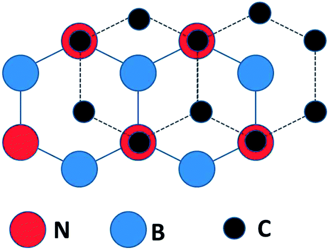 | ||
| Fig. 1 The C sites are alternatively directly over N sites or the centers of the B–N ring in the calculated lowest energy configuration for an isolated graphene/BN(0001) bilayer (after ref. 25). | ||
Experimental formation of graphene/BN bilayers has involved a number of approaches including physical transfer of graphene to BN crystallites,62–64 and direct growth by CVD of graphene on BN deposited by atomic layer deposition (ALD).65,66 Studies involving physically transferred graphene generally have not investigated the relative orientation of the bilayers, and revealed no evidence of a band gap in the graphene.46 For graphene not precisely in registry with the hexagonal boron nitride, the expectation is that a gap may be induced at the graphene “Dirac point” while a new superlattice of Dirac points develop at finite energy,26 yet such graphene overlayers exhibit very high mobilities of 25![[thin space (1/6-em)]](https://www.rsc.org/images/entities/char_2009.gif) 000 cm2 V−1 s−1 (ref. 62) to 37000 cm2 V−1 s−1 (ref. 67) and above, consistent with little or no band gap.
000 cm2 V−1 s−1 (ref. 62) to 37000 cm2 V−1 s−1 (ref. 67) and above, consistent with little or no band gap.
Graphene/BN bilayers with graphene and BN in registry with each other can be formed by direct growth on transition metal substrates. Typically the BN moiety consists of a monolayer resulting from self-limiting pyrolysis of borazine or similar precursors.67–79 However, graphene has been directly grown on BN(0001) nanoflakes by various methods.80,81 Graphene/BN bilayers formed by direct growth on Ni(111) (ref. 65) or Ru(0001) (ref. 65) do indicate that the graphene and BN sheets are in registry with each other, consistent with Fig. 1 and expectations,25 although the precise relative coordination of the two layers was not determined from the reported LEED data.
The metallic substrate can influence the BN electronic structure. This is manifest from a close inspection of the data in Fig. 2. The photoemission/inverse photoemission data (Fig. 2a) indicate no observable band gap at room temperature. This is consistent with the STM dI/dV data for the graphene/BN/Ru(0001) heterojunction (Fig. 2b) and the BN/Ru(0001) heterojunction prior to graphene growth (Fig. 2c) The scanning tunneling microscopy (STM) dI/dV data indicate significant Ru hybridization in valence and conduction bands of the BN monolayer (Fig. 2c): the BN monolayer, for example, exhibits a band gap of ∼2 eV compared to the 5.97 eV gap of bulk h-BN(0001).30,65
 | ||
| Fig. 2 The experimental density of states data for graphene/h-BN/Ru(0001) obtained from the combined PES and ARIPES data (a) and; (b) the STM dI/dV data (b). For comparison the STM dI/dV data for h-BN/Ru(0001) is also shown (c). All binding energies are referenced to the Fermi level as E − EF. From ref. 65. | ||
Consistent with the very small predicted band gap of 0.053 eV (53 meV) for graphene on boron nitride, the combined photoemission/inverse photoemission data (Fig. 2a) and the STM dI/dV data (Fig. 2b) show no evidence of a band gap in the (room temperature) density of states for graphene/h-BN/Ru(0001),30 but again substrate effects are difficult to completely exclude. The direct growth of graphene on multilayer BN may be expected to diminish the effects of the metal substrate interactions with the first BN overlayer, and afford a clearer understanding of graphene/BN interactions and large-area h-BN(0001) multilayers have been fabricated by atomic layer deposition.82
Misalignment of the graphene with a substrate, even a substrate like h-BN, can result from the graphene placement with respect to the substrate lattice. For graphene not grown in registry with the h-BN lattice, a Moiré pattern results as the crystallographic directions of the graphene rotated with respect to the substrate. In terms of electronic structure, this causes a folding of the graphene band structure in momentum space, potentially resulting in the replication of multiple Dirac points at symmetric densities away from the zero energy Dirac point.83–87 Worse yet, graphene bilayers, misaligned from one another might well result in something akin to a 2 dimensional electron gas.88 These misaligned graphene to h-BN or graphene to graphene bilayers represent weak van der Waals interactions, but strong interactions are also deleterious to formation of any band gap, such as introduced by a partial transition metal layer in close proximity to graphene,89,90 which leads to a density of states at the Fermi level.
C. Graphene on MgO(111)
It is not enough to simply open a band gap in graphene, as shown with graphene on SiC:28,40,91 as noted above, the chemical potential need not fall midgap as adsorbates or substrate interactions may also dope the graphene. More promising in this regard has been graphene on oxides (although not Al2O3 (ref. 60)) but where with the correct surface termination or oxide surface reconstruction, the graphene is no longer a gapless semiconductor, but an insulator.31,32,34,35 The low energy electron diffraction (LEED) data, in Fig. 3, indicates that graphene growth on the reconstructed surface of MgO(111) leads to a 1 monolayer (ML) graphene film that is actually of C3v symmetry rather than six-fold symmetry (Fig. 3a).29,30,32 This indicates that in the first layer, the chemical equivalence of the graphene A sites and B sites has been lifted, apparently due to interactions with the MgO substrate. This pattern of 3-fold symmetry is also observed for few-layer graphene on MgO(111),29,30,32 as seen in Fig. 3b. The formation of an oxidized carbon component coinciding with the onset of long-range order and a C3v LEED pattern strongly indicate that the graphene/MgO interface is commensurate and involves both an interfacial reconstruction and chemical reactions. Since the O–O nearest–neighbor distance in bulk-terminated MgO(111) is about 2.8 Å,92 an incommensurate graphene/oxide interface will result if the oxide surface does not reconstruct. Carbon A sites and B sites would thus experience an ensemble of different substrate environments, resulting in the same average environment at both A and B sites. Instead, the 3-fold symmetry observed for single and few-layer films,31 coincident with the formation of an oxidized carbon peak carbon 1s X-ray photoemission peak strongly suggests significant carbon and/or oxide reconstruction at the interface.30,32 Indeed, this first layer may not be pure “graphene”, but a partially oxidized, albeit ordered, form. | ||
| Fig. 3 The low energy electron diffraction (LEED) pattern of 1 ML graphene on MgO exhibits C3v symmetry, as illustrated in (a) where the background-subtracted intensities (arbitrary units) for ‘A’ and ‘B’ spots (circled) have an average intensity of 18.7 ± 3, and 12.9 ± 1 respectively. The uncertainties are the standard deviations. Other spots in the image are weaker and are attributed to multiple diffraction. The LEED pattern was acquired at 80 eV beam energy. (b) The intensity analysis of the average background-subtracted intensity (arbitrary units) LEED pattern (75 eV beam energy) of graphene film, 2.5 ML thick on MgO has the ‘A’ sites is 9.9 (±3), and that of the B sites is 7.5 (±0.9). From ref. 29 and 32. | ||
A band gap is evident in the combined photoemission and inverse photoemission,28,30,31 as seen in Fig. 2, for graphene on MgO(111), and although heavily p-doped by the oxide interface, this graphene is insulating. Charge transport data30,32 for a single layer C(111) film (produced by PVD) on MgO(111) are also shown in Fig. 4. Fig. 5 shows a logarithmic plot of the resistance as a function of reciprocal temperature, which is linear and exhibits the negative magnetoresistance characteristic of a nonmetal. The transport data yield a carrier-hopping activation energy of 0.64 (±0.05) eV,30,32 consistent with a band gap of 0.5 eV or greater that is estimated from the combined photoemission/inverse photoemission.31,32 Given that this picture is also evident in model calculations for single layer graphene between boron nitride layers,23 graphene on BN,25,27 SiO2,24 Al2O3(0001) (ref. 35) and MgO,34 and the possibly controversial53,54,91 experimental band gap for graphene on SiC,28,40 charge disorder or breaking of the A and B site symmetry matters.
 | ||
| Fig. 4 Angle-integrated valence band ultraviolet photoemission (UPS) (left) and k-vector resolved inverse photoelectron (right) spectroscopy data for a graphene film on MgO(111). The photoemission data correspond closely to spectra of graphene on transition metal substrates, but the data here indicate a band gap Eg of ∼0.5 eV. There is considerable uncertainty in the value of Eg due to the limited resolution of the inverse photoemission, as well as final state effects in both spectra. Binding energies are referenced to the Fermi level as E − EF. The π*, π, σ*, and σ weighted features indicated. Adapted from ref. 31. | ||
 | ||
| Fig. 5 Plot of ln(resistance) versus reciprocal temperature for single layer of C(111) on MgO(111). Data shows semiconducting behavior with a charge carrier hopping activation energy of ∼0.6 eV. Blue: data; black line: least squares fit. Adapted from ref. 32. | ||
Other oxides should be considered in the future, but identifying a suitable surface where there is an interface lattice match with graphene, as in the case of MgO(111), is a challenge. For graphene grown on Co3O4(111), there is no evidence of a band gap, and extensive p-doping of the graphene is likely.32,93 Chromia, i.e. Cr2O3, has potential to be more effective than MgO(111) if the interface is stable and suitably terminated. The attraction with chromia94,95 is the voltage controlled high surface polarization.96–98 Both the graphene Co3O4(111) and Cr2O3(001) to graphene interfaces are incommensurate, that is say that while graphene is aligned with the substrate when grown directly on Co3O4(111), the graphene lattice period is not identical with the substrate, at the interface. This makes symmetry reduction through different the chemical interactions at the graphene A and B sites more complex, if not more difficult. Cr2O3(001) is also attractive as having a less polar surface than MgO(111), thus less likely to p-dope the adjacent graphene layer extensively. As emphasized by Ballhausen,99 electrostatic crystal-field and quantum-mechanical ligand-field theories are equivalent as far as symmetry (and symmetry breaking) are concerned. The reason for MgO being an ideal substrate is the six-fold symmetry of the NaCl-type (111) plane in combination with interface (not bulk) lattice parameters that ensure epitaxial growth and a virtually complete AB splitting.
D. Band-gap formation in graphene through sublattice modification
The reduction of symmetry, by breaking the chemical equivalency of the graphene A and B sites, leads to a reduction in symmetry from C6v point group to the C3v point group. In the C3v point group, away from![[capital Gamma, Greek, macron]](https://www.rsc.org/images/entities/i_char_e0ba.gif) the center of the Brillouin zone, there is no mirror plane symmetry in the Brillouin zone line to K, the edge of the graphene Brillouin zone, about which the Dirac cone is centered. With the loss of mirror plane symmetry at K, the π band may not retain pure pz character, particularly if the graphene does not remains flat in the x–y plane as a result of the symmetry reduction. It should be recognized, as throughout surface science, there is an interplay between the energy cost or strain energy for a surface (and in this case graphene) structural reconstructions and reduction in energy opening up a band gap. More importantly, when a reduction of the symmetry is allowed, graphene can lower the total free energy of the system and a band gap will open at the Dirac point.
the center of the Brillouin zone, there is no mirror plane symmetry in the Brillouin zone line to K, the edge of the graphene Brillouin zone, about which the Dirac cone is centered. With the loss of mirror plane symmetry at K, the π band may not retain pure pz character, particularly if the graphene does not remains flat in the x–y plane as a result of the symmetry reduction. It should be recognized, as throughout surface science, there is an interplay between the energy cost or strain energy for a surface (and in this case graphene) structural reconstructions and reduction in energy opening up a band gap. More importantly, when a reduction of the symmetry is allowed, graphene can lower the total free energy of the system and a band gap will open at the Dirac point.
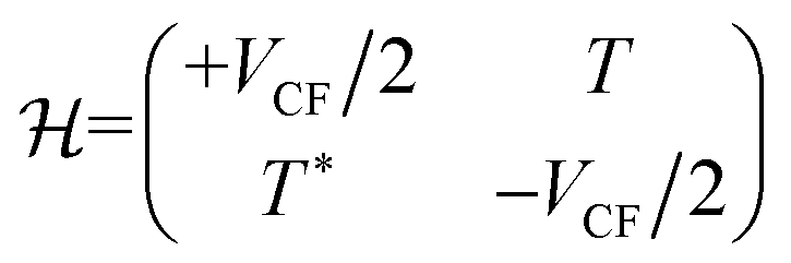
To explain how symmetry breaking substrates affect the band structure of graphene, we have modeled the substrate as a crystal-field source and treated the graphene as a tight-binding pz-electron system. As emphasized by Ballhausen99 as well as others,41 crystal-field and chemical effects are equivalent as far as symmetry-breaking is concerned, and the difference between the present theory and a more complete description of the electronic structure is the same as between Bethe-level crystal-field theory and ligand-field theory. For the theoretical background and the tight-binding calculation, see ref. 4, 41 and 100 and references therein.
Fig. 6 shows the considered structure, distinguishing between the two sublattices in graphene. The bright (A) and dark (B) atoms sit on top of crystallographically nonequivalent sites of the substrate, so that the orbital or “on-site” energies of the pz electrons are different. Ignoring a physically unimportant zero-point energy, the on-site energies for the A and B atoms are EA/B = ±VCF/2. Here the crystal-field parameter VCF increases with decreasing distance between graphene layer and substrate. The corresponding tight-binding Hamiltonian is
 | (1) |
exp(ik·RAB) describes the interatomic hopping between the A and B sites: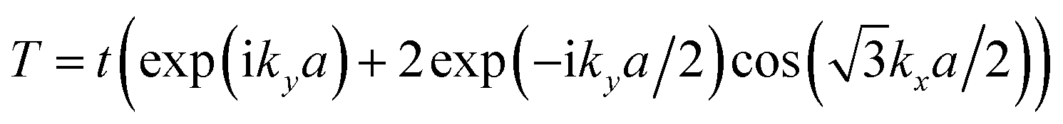 | (2) |
 | ||
| Fig. 6 Atomic structure of graphene. A-site atoms have B-site nearest neighbors only, and vice versa. In the present context, A (yellow) and B (red) atoms corresponds to different substrate positions. | ||
The appearance of T* in the bottom left corner of the Hamiltonian of eqn (1) is mandated by hermiticity, but it can also be interpreted in terms of interchanged sublattices (RAB = −RBA).
The solution of eqn (1) is trivial and yields two energy branches
 | (3) |
 | ||
| Fig. 7 The energy dispersion E+(kx, ky) for (a) perfect graphene (VCF = 0) and (b) graphene on a symmetry-breaking substrate (VCF = 2Vo = 0.8 t). | ||
Near any of the Dirac points (Kx, Ky), the energy can be expanded in terms of the small wave-vector difference q = (kx − Kx, ky − Ky). This leads to T*T = 3a2q2t2/4 where q = (qx2 + qy2)1/2, and the corresponding dispersion relation, E+ = VCF/2 + 3a2q2t2/4VCF, yields the effective mass m* = 2ℏ2VCF/3a2. Since the lattice parameter a does not vary very much from system to system, the effective mass is essentially determined by the band gap VCF. It is convenient to consider the ratio m*/m = 4VCEEHao2/3t2a2, where m is the electron mass, EH = 13.6 eV, and ao = 0.529 Å. Taking VCF = 0.5 eV, t = 2.7 eV, and a = 2.46 Å yields m*/m = 0.058, which can be regarded as a typical value for the effective mass. This is a smaller effective mass than is the case when the band gap is opened by uniaxial strain.4
Note that the gap is the same for all Dirac points (Fig. 8), that is, all spider legs have the same length. The difference between the A and B sites appears in the wave functions ψ±(r) corresponding to the two energy branches of eqn (3): at the Dirac points, the wave functions are entirely of the A type (ψ+) or of the B type (ψ−). For example, n-doping means that only A sites are occupied. In the absence of currents in the graphene sheet, the wave functions must be real. At the Dirac points, this can be achieved by superposing solutions for K and −K, exploiting that exp(iK·RA) + exp(−iK·RA) = 2cos(K·RA). Fig. 8 shows typical pz electron density that might be possible for graphene, as induced by the substrate. For n-doped graphene and positive VCF, the extra electrons occupies the A sites, and the electron density of the dark blue atoms is 4 times higher that of the bright blue atoms. For p-doped graphene, the same argument would of course apply to hole carriers.
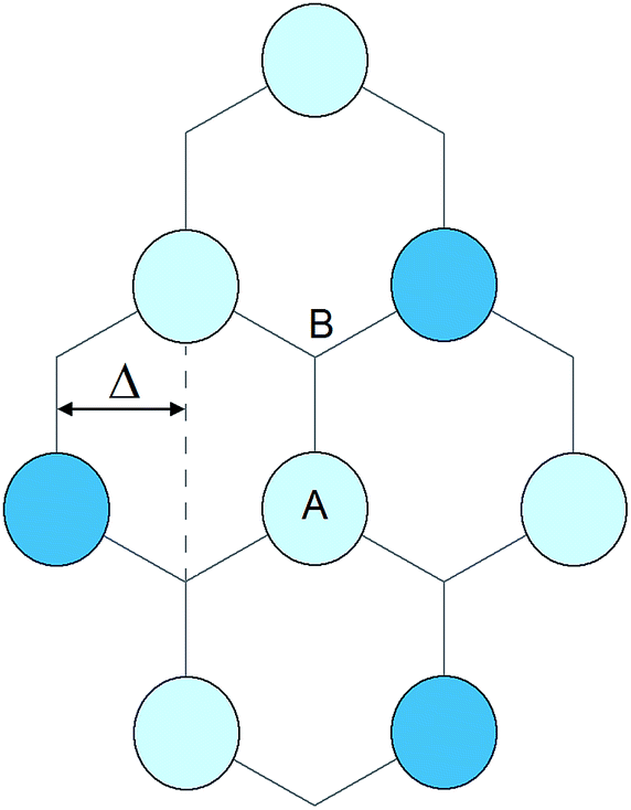 | ||
| Fig. 8 Schematic real-space electron density (top view of pz electrons) for n-doped graphene and positive VCF. | ||
For the derivation and interpretation of Fig. 8, it is convenient to use  . The horizontal distance between columns of atoms,
  , then corresponds to a phase shift of 2π/3 = 120°. This means a shift by 3Δ or 360° reproduces the original charge density. It should be noted that opening the band gap does result in an increase in carrier effective mass, and the greater the band gap, the greater the effective mass, as summarized in Fig. 9.
 | ||
| Fig. 9 The relationship of the band gap near the Dirac point and the relative on-site energies of the A and B sites by ±VCF/2. | ||
E. Conclusions
Band gap engineering of graphene is certainly possible, and this opens up the possibility of devices in very strict 2 dimensional conduction channels, but at the cost of increased effective mass. Effective mobilities for graphene on MgO have not been reported, but for graphene without a band gap (or at least a very nearly negligible band gap), transferred to various substrates, room temperature mobilities above ∼20000 cm2 V−1 s−1 (ref. 62, 63 and 101) are possible, but more often below 3000 cm2 V−1 s−1 are reported.52,102,103 While such mobility limitations are for the most part due to factors other than band structure,41,52,53,57,58,103 the introduction of a band gap can only further decrease carrier mobilities (Fig. 8 and 9).
It is important to realize that extrinsic mechanisms like adsorbate or substrate interactions may also dope the graphene. If the advantages accrued by converting graphene from a gapless semiconductor to a band gap semiconductor, it is important that the graphene then not be over-doped to imitate a degeneratively doped semiconductor. We note that there are flaws in estimating the band gap in graphene with density-functional theory (DFT): on the one hand, DFT is notorious for underestimating band gaps due to correlations, but on the other hand, wave-vector sampling techniques might not sample the density of states with a fine enough wave-vector grid and therefore overestimate a band gap. While correlation effects in graphene are debatable, our present approach explains band-gap openings in graphene with very high k-space accuracy.
Acknowledgements
This work was supported by the Semiconductor Research Corporation under tasks 2123.001 and 2358.001, and by C-SPIN, part of STARnet, a Semiconductor Research Corporation program sponsored by MARCO and DARPA (SRC 2381.002 and 2381.003). Further support was provided through the National Science Foundation funded Nebraska MRSEC DMR-0820521, the Army Research Office W911NF-10-2-0099, and the Nebraska Center for Materials and Nanoscience.Notes and references
- V. M. Pereira, A. H. C. Neto and N. M. R. Peres, Phys. Rev. B: Condens. Matter Mater. Phys., 2009, 80, 045401 CrossRef.
- G. Gui, J. Li and J. Zhong, Phys. Rev. B: Condens. Matter Mater. Phys., 2008, 78, 075435 CrossRef.
- I. I. Naumov and A. M. Bratkovsky, Phys. Rev. B: Condens. Matter Mater. Phys., 2011, 84, 245444 CrossRef.
- P. Kumar, R. Skomski, P. Manchanda, A. Kashyap and P. A. Dowben, Curr. Appl. Phys., 2014, 14, S136–S139 CrossRef PubMed.
- Y. W. Son, M. L. Cohen and S. G. Louie, Phys. Rev. Lett., 2006, 97, 216803 CrossRef.
- V. Barone, O. Hod and G. E. Scuseria, Nano Lett., 2006, 6, 2748–2754 CrossRef CAS PubMed.
- D. Prezzi, D. Varsano, A. Ruini, A. Marini and E. Molinari, Phys. Rev. B: Condens. Matter Mater. Phys., 2008, 77, 041404 CrossRef.
- L. Yang, M. L. Cohen and S. G. Louie, Nano Lett., 2007, 7, 3112–3115 CrossRef CAS PubMed.
- L. Yang, C. H. Park, Y. W. Son, M. L. Cohen and S. G. Louie, Phys. Rev. Lett., 2007, 99, 186801 CrossRef.
- D. Prezzi, D. Varsano, A. Ruini and E. Molinari, Phys. Rev. B: Condens. Matter Mater. Phys., 2011, 84, 041401 CrossRef.
- M. Y. Han, B. Özyilmaz, Y. Zhang and P. Kim, Phys. Rev. Lett., 2007, 98, 206805 CrossRef.
- X. Li, X. Wang, L. Zhang, S. Lee and H. Dai, Science, 2008, 319, 1229–1232 CrossRef CAS PubMed.
- S. Linden, D. Zhong, A. Timmer, N. Aghdassi, J. H. Franke, H. Zhang, X. Feng, K. Müllen, H. Fuchs, L. Chi and H. Zacharias, Phys. Rev. Lett., 2012, 108, 216801 CrossRef CAS.
- T. H. Vo, M. Shekhirev, D. A. Kunkel, M. D. Morton, E. Berglund, L. Kong, P. M. Wilson, P. A. Dowben, A. Enders and A. Sinitskii, Nat. Commun., 2014, 5, 3189 Search PubMed.
- K. Nakada, M. Fujita, G. Dresselhaus and M. S. Dresselhaus, Phys. Rev. B: Condens. Matter Mater. Phys., 1996, 54, 17954 CrossRef CAS.
- K. Wakabayashi, M. Fujita, H. Ajiki and M. Sigrist, Phys. Rev. B: Condens. Matter Mater. Phys., 1999, 59, 8271 CrossRef CAS.
- P. Sessi, J. R. Guest, M. Bode and N. P. Guisinger, Nano Lett., 2009, 9, 4343–4347 CrossRef CAS PubMed.
- R. Balog, B. Jørgensen, L. Nilsson, M. Andersen, E. Rienks, M. Bianchi, M. Fanetti, E. Lægsgaard, A. Baraldi, S. Lizzit, Z. Sljivancanin, F. Besenbacher, B. Hammer, T. G. Pedersen, P. Hofmann and L. Hornekær, Nat. Mater., 2010, 9, 315–319 CrossRef CAS PubMed.
- D. W. Boukhvalov and M. I. Katsnelson, J. Phys.: Condens. Matter, 2009, 21, 344205 CrossRef CAS PubMed.
- J. Berashevich and T. Chakraborty, Phys. Rev. B: Condens. Matter Mater. Phys., 2009, 80, 033404 CrossRef.
- S. Niyogi, E. Bekyarova, M. E. Itkis, H. Zhang, K. Shepperd, J. Hicks, M. Sprinkle, C. Berger, C. N. Lau, W. A. deHeer, E. H. Conrad and R. C. Haddon, Nano Lett., 2010, 10, 4061–4066 CrossRef CAS PubMed.
- J. Sławińska, I. Zasada, P. Kosiński and Z. Klusek, Phys. Rev. B: Condens. Matter Mater. Phys., 2010, 82, 085431 CrossRef.
- R. Quhe, J. Zheng, G. Luo, Q. Liu, R. Qin, J. Zhou, D. Yu, S. Nagase, W.-N. Mei, Z. Gao and J. Lu, NPG Asia Mater., 2012, 4, e6 CrossRef.
- P. Shemella and S. K. Nayak, Appl. Phys. Lett., 2009, 94, 032101 CrossRef PubMed.
- G. Giovannetti, P. A. Khomyakov, G. Brocks, P. J. Kelly and J. van den Brink, Phys. Rev. B: Condens. Matter Mater. Phys., 2007, 76, 073103 CrossRef.
- B. Hunt, J. D. Sanchez-Yamagishi, A. F. Young, M. Yankowitz, B. J. LeRoy, K. Watanabe, T. Taniguchi, P. Moon, M. Koshino, P. Jarillo-Herrero and R. C. Ashoori, Science, 2013, 340, 1427–1430 CrossRef CAS PubMed.
- M. Kindermann, B. Uchoa and D. L. Miller, Phys. Rev. B: Condens. Matter Mater. Phys., 2012, 86, 115415 CrossRef.
- S. Y. Zhou, G.-H. Gweon, A. V. Fedorov, P. N. First, W. A. de Heer, D.-H. Lee, F. Guinea, A. H. C. Neto and A. Lanzara, Nat. Mater., 2007, 6, 770–775 CrossRef CAS PubMed.
- S. Gaddam, C. Bjelkevig, S. Ge, K. Fukutani, P. A. Dowben and J. A. Kelber, J. Phys.: Condens. Matter, 2011, 23, 072204 CrossRef PubMed.
- J. A. Kelber, S. Gaddam, C. Vamala, S. Eswaran and P. A. Dowben, Proc. SPIE, 2011, 8100, 81000Y CrossRef PubMed.
- L. Kong, C. Bjelkevig, S. Gaddam, M. Zhou, Y. H. Lee, G. H. Han, H. K. Jeong, N. Wu, Z. Zhang, J. Xiao, P. A. Dowben and J. A. Kelber, J. Phys. Chem. C, 2010, 114, 21618–21624 CAS.
- J. A. Kelber, M. Zhou, S. Gaddam, F. L. Pasquale, L. M. Kong and P. A. Dowben, ECS Trans., 2012, 45, 49–61 CrossRef CAS PubMed.
- K.-A. Min, J. Park, J. Ryou, S. Hong and A. Soon, Curr. Appl. Phys., 2013, 13, 803–807 CrossRef PubMed.
- S. B. Cho and Y.-C. Chung, J. Mater. Chem. C, 2013, 1, 1595–1600 RSC.
- B. Huang, Q. Xu and S.-H. Wei, Phys. Rev. B: Condens. Matter Mater. Phys., 2011, 84, 155406 CrossRef.
- E. McCann, Phys. Rev. B: Condens. Matter Mater. Phys., 2006, 74, 161403 CrossRef.
- H. Min, B. Sahu, S. K. Banerjee and A. H. MacDonald, Phys. Rev. B: Condens. Matter Mater. Phys., 2007, 75, 155115 CrossRef.
- K. F. Mak, C. H. Lui, J. Shan and T. F. Heinz, Phys. Rev. Lett., 2009, 102, 256405 CrossRef.
- Y. Zhang, T.-T. Tang, C. Girit, Z. Hao, M. C. Martin, A. Zettl, M. F. Crommie, Y. R. Shen and F. Wang, Nature, 2009, 459, 820–823 CrossRef CAS PubMed.
- S. Y. Zhou, D. A. Siegel, A. V. Fedorov, F. El Gabaly, A. K. Schmid, A. H. Castro Neto, D.-H. Lee and A. Lanzara, Nat. Mater., 2008, 7, 259–260 CrossRef CAS.
- A. Bostwick, T. Ohta, J. L. McChesney, K. V. Emtsev, T. Seyller, K. Horn and E. Rotenberg, New J. Phys., 2007, 9, 385 CrossRef.
- G. Cocco, E. Cadelano and L. Colombo, Phys. Rev. B: Condens. Matter Mater. Phys., 2010, 81, 241412 CrossRef.
- S.-M. Choi, S.-H. Jhi and Y.-W. Son, Phys. Rev. B: Condens. Matter Mater. Phys., 2010, 81, 081407 CrossRef.
- Z. H. Ni, T. Yu, Y. H. Lu, Y. Y. Wang, Y. P. Feng and Z. X. Shen, ACS Nano, 2008, 2, 2301–2305 CrossRef CAS PubMed.
- K. S. Kim, Y. Zhao, H. Jang, S. Y. Lee, J. M. Kim, K. S. Kim, J.-H. Ahn, P. Kim, J.-Y. Choi and B. H. Hong, Nature, 2009, 457, 706–710 CrossRef CAS PubMed.
- Z. H. Ni, H. M. Wang, Y. Ma, J. Kasim, Y. H. Wu and Z. X. Shen, ACS Nano, 2008, 2, 1033–1039 CrossRef CAS PubMed.
- J. Hicks, A. Tejeda, A. Taleb-Ibrahimi, M. S. Nevius, F. Wang, K. Shepperd, J. Palmer, F. Bertran, P. Le Fèvre, J. Kunc, W. A. de Heer, C. Berger and E. H. Conrad, Nat. Phys., 2013, 9, 49–54 CrossRef CAS.
- Z. H. Chen, Y. M. Lin, M. J. Rooks and P. Avouris, Phys. E, 2007, 40, 228–232 CrossRef CAS PubMed.
- X. R. Wang, Y. Ouyang, L. Jiao, H. Wang, L. Xie, J. Wu, J. Guo and H. Dai, Nat. Nanotechnol., 2011, 6, 563–567 CrossRef CAS PubMed.
- Y. M. Lin, V. Perebeinos, Z. H. Chen and P. Avouris, Phys. Rev. B: Condens. Matter Mater. Phys., 2008, 78, 161409(R) CrossRef.
- K. Todd, H. T. Chou, S. Amasha and D. Goldhaber-Gordon, Nano Lett., 2009, 9, 416–421 CrossRef CAS PubMed.
- J. Baringhaus, M. Ruan, F. Edler, A. Tejeda, M. Sicot, A. Taleb-Ibrahimi, A.-P. Li, Z. Jiang, E. H. Conrad, B. Berger, C. Tegenkamp and W. A. de Heer, Nature, 2014, 506, 349 CrossRef CAS PubMed.
- E. Rotenberg, A. Bostwick, T. Ohta, J. L. McChesney, T. Seyller and K. Horn, Nat. Mater., 2008, 7, 258–259 CrossRef CAS PubMed.
- T. Ohta, A. Bostwick, J. L. McChesney, T. Seyller, K. Horn and E. Rotenberg, Phys. Rev. Lett., 2007, 98, 206802 CrossRef.
- F. Varchon, R. Feng, J. Hass, X. Li, B. Ngoc Nguyen, C. Naud, P. Mallet, J.-Y. Veuillen, C. Berger, E. H. Conrad and L. Magaud, Phys. Rev. Lett., 2007, 99, 126805 CrossRef CAS.
- V. W. Brar, Y. Zhang, Y. Yayon, T. Ohta, J. L. McChesney, A. Bostwick, E. Rotenberg, K. Horn and M. F. Crommie, Appl. Phys. Lett., 2007, 91, 122102 CrossRef PubMed.
- E. H. Hwang and S. Das Sarma, Phys. Rev. B: Condens. Matter Mater. Phys., 2007, 75, 205418 CrossRef.
- A. Bostwick, T. Ohta, T. Seyller, K. Horn and E. Rotenberg, Nat. Phys., 2007, 3, 36–40 CrossRef CAS.
- Y. Qi, S. H. Rhim, G. F. Sun, M. Weinert and L. Li, Phys. Rev. Lett., 2010, 105, 085502 CrossRef CAS.
- M. A. Fanton, J. A. Robinson, C. Puls, Y. Liu, M. J. Hollander, B. E. Weiland, M. LaBella, K. Trumbull, R. Kasarda, C. Howsare, J. Stitt and D. W. Snyder, ACS Nano, 2011, 5, 8062–8069 CrossRef CAS PubMed.
- A. H. C. Neto, F. Guinea, N. M. R. Peres, K. S. Novoselov and A. K. Geim, Rev. Mod. Phys., 2009, 81, 109 CrossRef.
- C. R. Dean, A. F. Young, I. Meric, C. Lee, L. Wang, S. Sorgenfrei, K. Watanabe, T. Taniguchi, P. Kim, K. L. Shepard and J. Hone, Nat. Nanotechnol., 2010, 5, 722–726 CrossRef CAS PubMed.
- W. Gannett, W. Regan, K. Watanabe, T. Taniguchi, M. F. Crommie and A. Zettl, Appl. Phys. Lett., 2011, 98, 242105 CrossRef PubMed.
- N. Petrone, C. R. Dean, I. Meric, A. M. van der Zande, P. Y. Huang, L. Wang, D. Muller, K. L. Shepard and J. Hone, Nano Lett., 2012, 12, 2751–2756 CrossRef CAS PubMed.
- C. Bjelkevig, Z. Mi, J. Xiao, P. A. Dowben, L. Wang, W.-N. Mei and J. A. Kelber, J. Phys.: Condens. Matter, 2010, 22, 302002 CrossRef PubMed.
- C. Oshima, A. Itoh, E. Rokuta, T. Tanaka, K. Yamashita and T. Sakurai, Solid State Commun., 2000, 116, 37–40 CrossRef CAS.
- T. Brugger, S. Günther, B. Wang, J. H. Dil, M.-L. Bocquet, J. Osterwalder, J. Wintterlin and T. Greber, Phys. Rev. B: Condens. Matter Mater. Phys., 2009, 79, 045407 CrossRef.
- A. B. Preobrajenski, A. S. Vinogradov and N. Mårtensson, Surf. Sci., 2005, 582, 21–30 CrossRef CAS PubMed.
- A. Goriachko, Y. B. He and H. Over, J. Phys. Chem. C, 2008, 112, 8147–8152 CAS.
- M. L. Ng, A. B. Preobrajenski, A. S. Vinogradov and N. Mårtensson, Surf. Sci., 2008, 602, 1250–1255 CrossRef CAS PubMed.
- A. Goriachko, Yunbin, M. Knapp and H. Over, Langmuir, 2007, 23, 2928–2931 CrossRef CAS PubMed.
- M. Morscher, M. Corso, T. Greber and J. Osterwalder, Surf. Sci., 2006, 600, 3280–3284 CrossRef CAS PubMed.
- W. Auwärter, T. J. Kreutz, T. Greber, J. Osterwalder, M. Corso, T. Brugger, S. Berner, J. Osterwalder and T. Greber, Surf. Sci., 1999, 429, 229–236 CrossRef.
- M. Muntwiler, M. Hengsberger, A. Dolocan, H. Neff, T. Greber and J. Osterwalder, Phys. Rev. B: Condens. Matter Mater. Phys., 2007, 75, 075407 CrossRef.
- M. Muntwiler, W. Auwärter, F. Baumberger, M. Hoesch, T. Greber and J. Osterwalder, Surf. Sci., 2001, 472, 125–132 CrossRef CAS.
- Y. Gamou, M. Terai, A. Nagashima and C. Oshima, Sci. Rep. Res. Inst., Tohoku Univ., Ser. A, 1997, 44, 211 CAS.
- A. Nagashima, N. Tejima, Y. Gamou, T. Kawai and C. Oshima, Phys. Rev. Lett., 1995, 75, 3918 CrossRef CAS.
- A. Nagashima, N. Tejima, Y. Gamou, T. Kawai and C. Oshima, Phys. Rev. B: Condens. Matter Mater. Phys., 1995, 51, 4606 CrossRef CAS.
- K. Zumbrägel, K. Wulff, C. Eibl, M. Donath and M. Hengsberger, Phys. Rev. B: Condens. Matter Mater. Phys., 2008, 78, 085422 CrossRef.
- T. Lin, Y. Wang, H. Bi, D. Wan, F. Huang, X. Xie and M. Jiang, J. Mater. Chem., 2012, 22, 2859–2862 RSC.
- X. Ding, G. Ding, X. Xie, F. Huang and M. Jiang, Carbon, 2011, 49, 2522–2525 CrossRef CAS PubMed.
- J. A. Kelber, Direct Graphene Growth on Dielectric Substrates, Graphene, Carbon Nanotubes and Nanostructures: Techniques and Applications, CRC Press, 2013, ch. 5, pp. 89–113 Search PubMed.
- M. Yankowitz, J. Xue, D. Cormode, J. D. Sanchez-Yamagishi, K. Watanabe, T. Taniguchi, P. Jarillo-Herrero, P. Jacquod and B. J. LeRoy, Nat. Phys., 2012, 8, 382–386 CrossRef CAS.
- C. H. Park, L. Yang, Y.-W. Son, M. L. Cohen and S. G. Louie, Nat. Phys., 2008, 4, 213–217 CrossRef CAS.
- C. H. Park, L. Yang, Y.-W. Son, M. L. Cohen and S. G. Louie, Phys. Rev. Lett., 2008, 101, 126804 CrossRef.
- L. Brey and H. A. Fertig, Phys. Rev. Lett., 2009, 103, 046809 CrossRef CAS.
- P. Burset, A. Yeyati, L. Brey and H. Fertig, Phys. Rev. B: Condens. Matter Mater. Phys., 2011, 83, 195434 CrossRef.
- R. V. Gorbachev, A. K. Geim, M. I. Katsnelson, K. S. Novoselov, T. Tudorovskiy, I. V. Grigorieva, A. H. MacDonald, S. V. Morozov, K. Watanabe, T. Taniguchi and L. A. Ponomarenko, Nat. Phys., 2012, 8, 896–901 CrossRef CAS.
- Y. Li, P. Chen, G. Zhou, J. Li, J. Wu, B.-L. Gu, S. B. Zhang and W. Duan, Phys. Rev. Lett., 2012, 109, 206802 CrossRef.
- J. Zhou, L. Wang, R. Qin, J. Zheng, W.-N. Mei, P. Dowben, S. Nagase, Z. Gao and J. Lu, J. Phys. Chem. C, 2011, 115, 25273–25280 CAS.
- T. Ohta, A. Bostwick, J. L. McChesney, T. Seyller, K. Horn and E. Rotenberg, Phys. Rev. Lett., 2007, 98, 206802 CrossRef.
- V. K. Lazarov, R. Plass, H.-C. Poon, D. K. Saldin, M. Weinert, S. A. Chambers and M. Gajdardziska-Josifovska, Phys. Rev. B: Condens. Matter Mater. Phys., 2005, 71, 115434 CrossRef.
- M. Zhou, F. L. Pasquale, P. A. Dowben, A. Boosalis, M. Schubert, V. Darakchieva, R. Yakimova, L. Kong and J. A. Kelber, J. Phys.: Condens., 2012, 24, 072201 CrossRef PubMed.
- X. Chen, H. Kazi, Y. Cao, B. Dong, F. L. Pasquale, J. A. Colón Santana, S. Cao, R. Welch, Ch. Binek, A. Enders, J. A. Kelber and P. A. Dowben, Mater. Chem. Phys. Search PubMed , submitted.
- S. Stuart, E. Sachet, J. P. Maria, J. E. Rowe, M. C. Ulrich and D. Dougherty, http://meetings.aps.org/link/BAPS.2014.MAR.F6.5, Bulletin of the American Physical Society, 2014, F6.5.
- X. He, Y. Wang, N. Wu, A. N. Caruso, E. Vescovo, K. D. Belashchenko, P. A. Dowben and Ch. Binek, Nat. Mater., 2010, 9, 579–585 CrossRef CAS PubMed.
- N. Wu, X. He, A. Wysocki, U. Lanke, T. Komesu, K. D. Belashchenko, Ch. Binek and P. A. Dowben, Phys. Rev. Lett., 2011, 106, 087202 CrossRef.
- S. Cao, X. Zhang, N. Wu, A. T. N'Diaye, G. Chen, A. K. Schmid, X. Chen, W. Echtenkamp, A. Enders, Ch. Binek and P. A. Dowben, New J. Phys., 2014, 16, 073021 CrossRef.
- C. J. Ballhausen, Ligand Field Theory, McGraw-Hill, New York, 1962 Search PubMed.
- S. Reich, J. Maultzsch, C. Thomsen and P. Ordejn, Phys. Rev. B: Condens. Matter Mater. Phys., 2002, 66, 035412 CrossRef.
- S. Kim, J. Nah, I. Jo, D. Shahrjerdi, L. Colombo, Z. Yao, E. Tutuc and S. K. Banerjee, Appl. Phys. Lett., 2009, 94, 062107 CrossRef PubMed.
- H. Lv, H. Wu, K. Xiao, W. Zhu, H. Xu, Z. Zhang and H. Qian, Appl. Phys. Lett., 2013, 102, 183107 CrossRef PubMed.
- D. K. Ferry, J. Comput. Electron., 2013, 12, 76–84 CrossRef CAS PubMed.
| This journal is © The Royal Society of Chemistry 2014 |