Silk/molecular conductor bilayer thin-films: properties and sensing functions†
Eden
Steven
*a,
Victor
Lebedev
b,
Elena
Laukhina
*bc,
Concepció
Rovira
bc,
Vladimir
Laukhin
bcd,
James S.
Brooks
a and
Jaume
Veciana
bc
aDepartment of Physics, National High Magnetic Field Laboratory Florida State University, 1800 East Paul Dirac Drive, Tallahassee, Florida 32310, USA
bInstitut de Ciéncia de Materials de Barcelona (ICMAB-CSIC), Campus UAB, Bellaterra, 08193, Spain
cCIBER de Bioingeniería, Biomateriales y Nanomedicina (CIBER-BBN), Campus UAB, Bellaterra, 08193, Spain
dInstitució Catalana de Recerca i Estudis Avançats (ICREA), ICMAB-CSIC, Campus UAB, Bellaterra, 08193, Spain. E-mail: esteven@magnet.fsu.edu; laukhina@icmab.es
First published on 3rd June 2014
Abstract
Since their discovery, organic conductors have attracted fundamental and device physics interest due to their diverse physical properties. However, conventional electrochemical growth methods produce millimeter-sized crystals that do not translate to the fabrication of large-scale thin-film devices. Of late a chemical-vapor annealing method has been proved to be capable of growing a conductive polycrystalline layer of (BEDT-TTF)2I3 molecular conductor on the surface of soluble polycarbonate (PC) thin films in a bilayer configuration. (Here BEDT-TTF = bis(ethylenedithio)tetrathiafulvalene.) This has resulted in efficient piezoresistive organic molecular sensors. Conversely, solubility and other incompatibilities limit the direct application of the crystallite growth method to other substrates with arbitrary shape and composition. Here we report methods to circumvent these limitations. Specifically, we demonstrate the transfer of the active layer of a PC/(BEDT-TTF)2I3 bilayer film from the non-porous parent PC substrate to porous and humidity-dependent Bombyx mori silk target substrates. SEM analysis, temperature dependent resistance, and electromechanical measurements show no significant damage to the transferred (BEDT-TTF)2I3 layer. The silk/(BEDT-TTF)2I3 bilayer films exhibit additional functions that can be used for humidity sensing, electric current-driven actuators, and strain detection. Of particular significance is the piezoresistive function of the porous silk bilayer structure that allows the investigation of multi-stage diffusion processes.
Conceptual insightsA polycrystalline layer of piezoresistive (BEDT-TTF)2I3-based molecular conductor is transferred from the parent polycarbonate/(BEDT-TTF)2I3 bilayers to silk and other substrates with various shapes and compositions. The transferred layer is robust as confirmed by SEM, temperature dependent resistance, and electromechanical measurements. The silk/(BEDT-TTF)2I3 bilayer films are sensitive to moisture, allowing their use for humidity sensing, electrical current driven actuators, and the study of complex moisture diffusion processes. |
Introduction
Organic molecular conducting materials are well known for their high quality single crystalline form, and for having a wide range of physical properties including insulating, semiconducting, metallic, magnetic and superconducting phases.1–9 Most often, these materials are formed as charge transfer salts in the form D2A, where D+1/2 is a planar organic donor, and A−1 is an acceptor; as a result the D2A salt has unfilled bands and is metallic at room temperature.10–13 Until recently, the soft-organic and small-sized (∼1 mm3) nature of single crystals and the dendritic bulk morphology of electrochemical growth by oxidation methods have prohibited any standard method of scale-up processing into thin films for device or sensor applications. A breakthrough14–16 came with the discovery that the oxidation reaction could proceed by mixing the donor component BEDT-TTF (bis(ethylenedithio)tetrathiafulvalene) in its neutral state into a polycarbonate (PC) thin film that then is exposed to an acceptor like iodine, expressed in a solvent vapor. This produced a self-assembling polycrystalline layer composed of physically and electronically interconnected sub-micron crystallites on the top of the exposed surface of the PC film, which respond reliably to bending strain,17 yielding a new class of flexible organic molecule-based sensors.18,19Unfortunately, the chemical growth method is compatible only with solvent soluble polymer substrates, prohibiting its direct use to cover substrates of interest with variable (sculpted) shapes and compositions. For example, it is very difficult to infuse the BEDT-TTF molecules into silk materials homogeneously prior to the oxidation due to either solvent incompatibilities or the tendencies of the BEDT-TTF molecules to crystallize in silk environments prior to the oxidation process (see ESI, Fig. S1†). The purpose of the present work is to show how the functional thin polycrystalline layers can be transferred from a non-porous PC substrate to a substrate that has both shape and humidity-dependent functions, setting the stage for future applications of molecular conductors. Here we demonstrate methods of transferring the active layer of highly piezoresistive PC/(BEDT-TTF)2I3 (pristine) bilayer films from the parent PC substrate to Bombyx mori silk film target substrates.
The (BEDT-TTF)2I3 salt can be obtained in five different crystal phases, two of which are more common, α- and β-(BEDT-TTF)2I3, where the semimetal α-phase and superconducting β-phase are semiconducting and metallic as polycrystalline layers, respectively.15 The transferred (BEDT-TTF)2I3 layers (for both α- and β-phases) are robust, exhibiting similar surface and electrical properties to those of the pristine bilayers as confirmed by SEM, temperature dependent resistance, and electromechanical measurements. In comparison to the pristine bilayer films, the silk/(BEDT-TTF)2I3 bilayer films exhibit additional functions, allowing electronic monitoring of humidity and electrical current actuated functions (see ESI, Movie S1†). A unique aspect of this novel silk bilayer structure is that the humidity dependent resistance provides new ways to address complex diffusion effects in porous substrates such as the Bombyx mori silk film. By correlating moisture-induced changes in the silk structure to the piezoresistive properties of the (BEDT-TTF)2I3 layer, a non-Fickian, multi-stage moisture absorption process in the silk layer is revealed. In addition to silk substrates, the layer transfer can also be directly applied to rubber, silica, glass, sculpted plastic products, paper, and substrates with various shapes and geometry.
Results and discussion
In the present work we have used PC/(BEDT-TTF)2I3 bilayer films with the α-(BEDT-TTF)2I3 salt for strain studies. By heat treatment of such bilayer films, the α-(BEDT-TTF)2I3 active layer can be transformed into a more thermodynamically stable β-(BEDT-TTF)2I3 active layer15 which we have used for humidity studies and electrical current actuator demonstrations. Both (referred to generically as (BEDT-TTF)2I3) are electrically conducting and piezoresistive at room temperature. To cover different substrates with (BEDT-TTF)2I3 active layers, we have developed two different procedures (Fig. 1) to transfer the (BEDT-TTF)2I3 layers grown at the surface of a parent PC support to receiving substrates.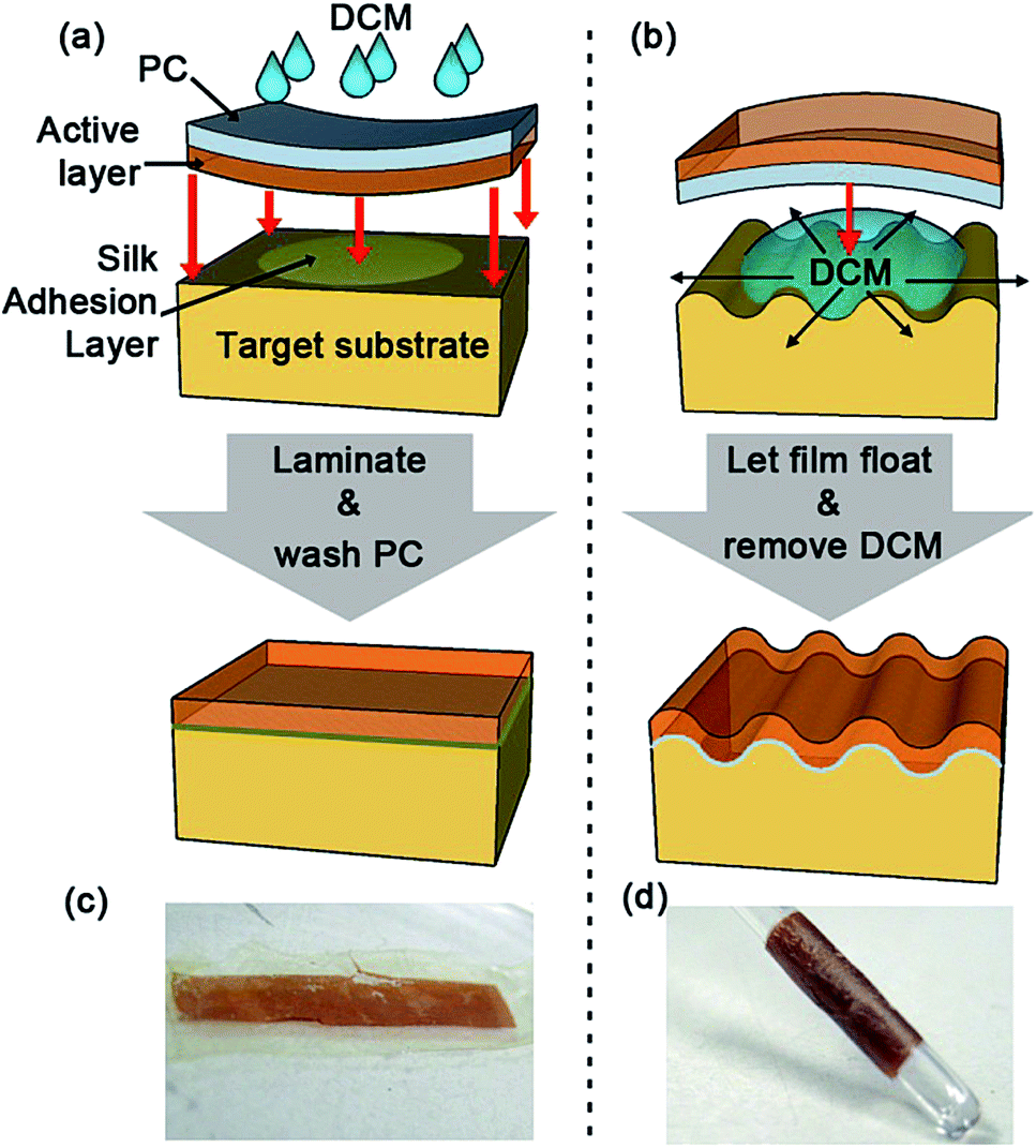 | ||
| Fig. 1 Layer transfer schematics. Overview of the (a) face-down and (b) face-up layer transfer methods. Photographs of the transferred strain sensing layer of α-(BEDT-TTF)2I3 molecular semimetal (c) to a silk film via a face-down approach and (d) to a glass tube of ∅ 3 mm via a face-up approach. | ||
The first procedure, referred hereafter to as the face-down layer transfer, where the active layer face of the pristine bilayer is oriented down toward the receiver substrate, is most suitable for covering various flat substrates (Fig. 1a and c). The second procedure, namely the face-up layer transfer (active layer face oriented up and away from the receiver substrate), is more universal; it allows the covering of sculpted substrates (Fig. 1b and d). In both cases, the transfer involves the separation of the (BEDT-TTF)2I3 layers from a parent PC substrate by dissolving the PC layer using a small amount of dichloromethane (DCM). Additional experimental details are given in the ESI (Fig. S2–S8†).
Face-down layer transfer
The applicability of the face-down approach of covering substrates with molecular metals (see ESI, Fig. S2 and S3†) is considered in detail using examples of the (BEDT-TTF)2I3 layer transfer from a parent PC support to a receiver Bombyx mori silk film; a material considered as one of the ideal substrates for implantable devices.20,21 The silk film is prepared via drop casting an ∼8% (w/v) solution of silk in water on a polystyrene dish. The silk solution is obtained by following the procedure reported in ref. 22, which involves the fiber extraction from raw Bombyx mori cocoons (purchased from Aurora Silk) using a 0.02 M Na2CO3 solution, followed by fiber dissolving in a 9.3 M LiBr solution, purification by dialysis (Slide-A-Lyzer G-2 dialysis cassette, 3500 MWCO), and low temperature centrifugation.To cover the silk film with a (BEDT-TTF)2I3 layer using the face-down layer transfer (see ESI, Fig. S2 and S3†), the silk film is first water-annealed23 for 24 hours at 50 mbar to render it insoluble in water. Then, a thin Bombyx mori silk solution is deposited on the silk film to act as an adhesive layer. The bilayer (BL) films are laminated onto the wet silk surface by putting the top conductive (BEDT-TTF)2I3 layer of the BL film face down on the substrate. The conductive layer of the BL film can be pre-treated by argon plasma for 10 seconds to improve its homogeneous adhesion to the receiver silk film. Lamination is completed by using a commercial smooth polytetrafluoroethylene-based plate. To remove the PC layer, we drop DCM over the film at an angle to allow the solvent containing dissolved PC to flow away. The complete removal of the PC layer can be checked by either measuring the electrical resistance of the film or through direct observation under an optical microscope (see ESI, Fig. S4†).
Surface and interface structures
The face-down layer transfer allowed us for the first time to study the texture of the reverse side of the conductive α-(BEDT-TTF)2I3 layer formed at the interface with the PC film. Micro-scale surface analysis was performed using a SEM (Quanta FEI 200 FEG-ESEM) with an energy dispersive X-ray (EDX) spectrometer. As presented in Fig. 2a, we observed a small number of crystallite aggregates (zone b) on the reverse side of the otherwise smooth conducting layer (zone a). Using EDX analysis the contribution of elemental I and S atoms to the composition of zone a was found to be (18.2 ± 0.5) and (81.8 ± 0.5) atomic%, respectively.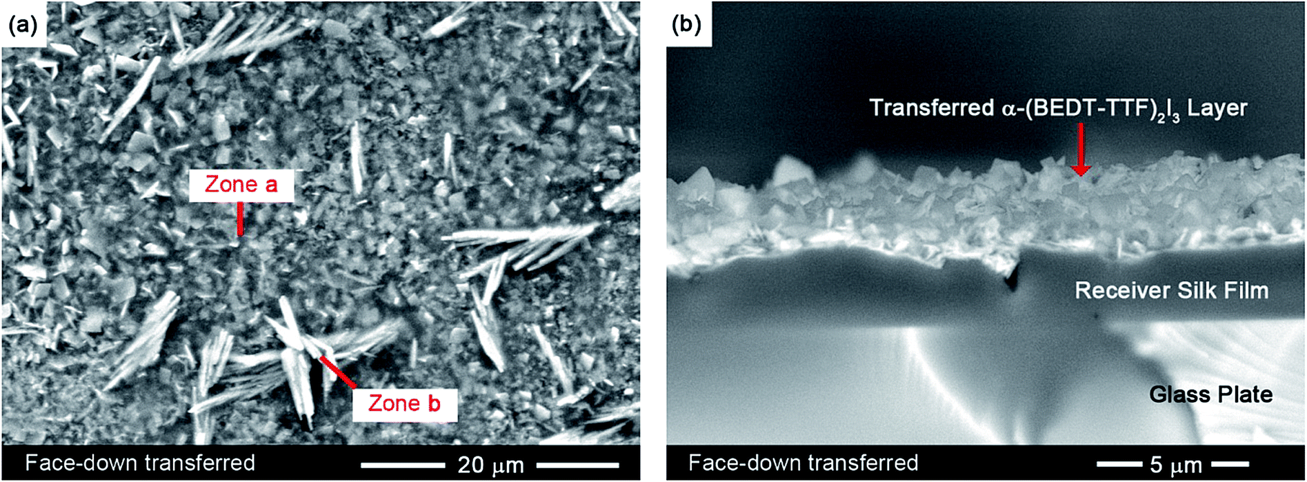 | ||
| Fig. 2 SEM images of face-down transferred α-(BEDT-TTF)2I3 layers. (a) Surface and (b) cross-section profile of a silk/α-(BEDT-TTF)2I3 bilayer; the silk film was cast on a glass slide. The surface profile reveals the back side arrangement of the conductive α-(BEDT-TTF)2I3 layer initially formed on the parent PC film. Zones a and b correspond to the reacted and un-reacted (BEDT-TTF) compound, respectively. | ||
Therefore, zone a has an average (BEDT-TTF)2I3.5 composition that is in reasonable agreement with the expected stoichiometric formula α-(BEDT-TTF)2I3. In contrast, zone b contains a very small amount of iodine: the contribution of I and S to their compositions was found to be (1.5 ± 0.5) and (98.5 ± 0.5) atomic%, respectively. Based on this observation, the minor crystallite aggregates of crystals have average (BEDT-TTF)I0.1 composition. This suggests that during the BL film preparation,13–15 un-reacted BEDT-TTF may crystallize on the back side of the conductive layer.
The cross-section of the silk/α-(BEDT-TTF)2I3 bilayer was also studied by SEM. As is evident from Fig. 2b, the transferred α-(BEDT-TTF)2I3-based layer has a good intimate contact with the receiver silk film similar to that of the pristine PC/α-(BEDT-TTF)2I3 bilayer films. Using the same film lamination principle, the face-down layer transfer may be used for covering various flat substrates including paper sheets; the paper sheets can be covered with combinations of α- and β-(BEDT-TTF)2I3 as desired to form conductive sensing paper (see ESI, Fig. S5 and S6†).
Electronic properties
In addition to similar surface and interfacial structures, the silk/(BEDT-TTF)2I3 and PC/(BEDT-TTF)2I3 bilayer films also exhibit similar temperature dependent resistance and electromechanical behavior. The α- and β-(BEDT-TTF)2I3 layers before and after layer transfer were examined by four probe direct current (DC) resistance measurements with carbon paste electrodes using a Keithley 6221 current source and a Keithley 2182A nanovoltmeter. As is evident in Fig. 3a and b, both original (PC) and transferred (silk) α- and β-(BEDT-TTF)2I3 layers demonstrate basically the same temperature-dependent electronic transport properties. It should be noted that in comparison with the original PC/α-(BEDT-TTF)2I3 layer, the silk/α-(BEDT-TTF)2I3 transferred layer exhibits a slightly broader semimetal-to-insulator transition. | ||
| Fig. 3 Electronic and electromechanical properties of the face-down transferred sensing layer. Temperature dependence of the normalized resistance of the original (PC – solid line) and transferred (silk – dashed line) layers of (a) α- and (b) β-(BEDT-TTF)2I3. (c) Resistance changes of the transferred silk/α-(BEDT-TTF)2I3 layer with time upon an application of 7 cycles of monoaxial elongations performed at a strain rate of 0.3 μm s−1. The layer was transferred on a silk film using the face-down transfer approach. Resistance and elongation data were obtained every 0.5 s during the multi-cyclic deformation on a film with a length of 1.2 cm. | ||
The data presented in Fig. 3c show that the electrical resistance of the transferred α-(BEDT-TTF)2I3 layer on a silk film exhibits a reversible linear response to relative strain (ε). The value of strain sensitivity (gauge factor) is 9, in good agreement with previously reported values.9 The gauge factor is defined as the ratio between the relative resistance change (ΔR/R0) and the relative strain value (ε = ΔL/L0), where ΔR = R − R0, ΔL = L − L0, R is the resistance at length L after elongation, and R0 is the resistance at the initial gauge length L0.
Humidity dependence
In contrast to the pristine PC/(BEDT-TTF)2I3 bilayer film, the silk/(BEDT-TTF)2I3 BL film exhibits electric current-actuated functions (see ESI, Movie S1†) and a humidity dependent resistance. Due to the softness of the piezoresistive molecular conductor crystals and their intimate contact with the silk substrate, the resistance is well-coupled to the swelling/de-swelling of the silk substrate under varying humidity conditions. This also allows us to study the water absorption mechanism of Bombyx mori silk via electrical transport measurements. The humidity dependent resistance measurement was performed inside an environmental chamber at 23 °C in a 4-contact configuration using a lock-in amplifier (see ESI, Fig. S9†). A separate humidity sensor (HIH-5030) was mounted in close proximity to the BL film.As is evident in Fig. 4a, the resistance of the BL film reversibly tracks the relative humidity (RH) changes in the surrounding environment. A delay in the humidity response is observed (Fig. 4b) even though the RH is varied slowly (∼0.025% per s), indicating a diffusion-limited moisture absorption process of the Bombyx mori silk film. The humidity response can be modelled by considering the general solution to a resistor–capacitor (RC) charging circuit where the charging voltage varies with time. In this model (eqn (1)), for any specific time t, the supply voltage Vs is analogous to RH, the capacitor voltage Vc is analogous to the moisture uptake (and swelling of the silk that produces a change in the film resistance), Vr is the initial capacitor voltage (analogous to the initial moisture content) at the start of the charging process, and τ is the diffusion relaxation time constant analogous to RC. In equilibrium and/or for τ ≥ 0, the moisture uptake (∼Vc) is directly proportional to the RH (∼Vs). Since in the bilayer film we measure the piezoresistance which is analogous to the capacitor voltage, we may recast eqn (1) as eqn (2a) under the assumption in eqn (2b) that RH drives the time dependence.
| Vc(t) = Vs(t)(1 − e−t/τ) + Vre−t/τ | (1) |

| R(t) − R0 = Rs(t)(1 − e−t/τ) + Rre−t/τ | (2a) |
| Rs(t) = ARH(t) | (2b) |
 | ||
| Fig. 4 Humidity monitoring via electrical response of Bombyx mori silk/β-(BEDT-TTF)2I3. (a) Cyclic RH monitoring. Maximum RH sweep rate ∼0.025% per s. (b) Fit to the data using a capacitor charging model. (c) Time dependent resistance of a flash humidity exposed BL film at 23 °C and 73% RH. Inset: log–log plot of the normalized resistance vs. time. The value of power factor, n, is extracted from the slope indicated by the dotted line. (d) Fick t1/2 plot of the time dependent resistance during the step-function humidity exposure. | ||
Explicitly, the analogy is that R(t) is the resistance of the BL film at any given time, R0 is the resistance of a completely dried film, Rs(t) is the resistance of the saturated film at a given RH value, Rr is the resistance due to the trapped residual moisture content at the beginning of the absorption process, and τ is the time constant of the humidity response. In Fig. 4b, R0, Rr, proportionality constant A, and τ are determined to be 6.8 kΩ, 1 kΩ, 33.4 Ω per RH%, and 645 s.
Although this model fits well to the data in Fig. 4b, the model breaks down at faster sweep rates. For the measurement obtained at a higher RH rate (0.125% per s), it is not possible to fit the data perfectly using the model (see ESI, Fig. S10†). This leads us to believe that the moisture absorption process is more complex than that described by the simple RC circuit model.
To study the moisture absorption process in more detail, a step function exposure experiment was performed. The BL film was first dried overnight at 23 °C and 30% RH, after which the film was suddenly exposed to a constant, saturated 73% RH environment. In Fig. 4c, the time dependent resistance after the sudden exposure is presented, showing features that deviate from the Fickian moisture absorption process.24,25 First, there is no clear saturation level26 that is typically observed in a Fickian process, at least within the given time scale. Instead, the resistance continues to slowly increase at longer times. Second, the normalized resistance (ΔR(t)/ΔRmax) varies with time (t) according to the following function, ΔR(t)/ΔRmax ∼ tn, where ΔR(t) = R(t) − R(at 30% RH), ΔRmax = R(at 73% RH) − R(at 30% RH), and n = 0.83 (Fig. 4c). In a Fickian process, n = 0.5 at the initial stage of absorption.24,27 These features are similar to the cases reported in the literature26 involving a dual-stage moisture diffusion process,25,26 where the first and second stages are attributed to void-filling and hydrogen bonding processes.28 As shown in Fig. 4d, there are 3 distinct stages of diffusion. The first stage can be attributed to film expansion mainly due to the filling of voids in the silk film. As the absorption transitions to the second stage, moisture continues to fill the voids but also penetrates and forms hydrogen bonds with the silk protein, swelling the protein internally. Finally in the third stage, all the voids have been filled but internal swelling continues to progress deeper into the silk structures. This result highlights the complex mechanisms of water transport processes in Bombyx mori silk.
Face-up layer transfer
For applications requiring the covering of sculpted substrates (see ESI, Fig. S7 and S8†), the face-up approach is used, where the top conductive (BEDT-TTF)2I3 layer of the bilayer films faces up on the substrate. Whereas the face-down layer transfer relies on the effectiveness of mechanical lamination, the face-up layer transfer is based on the thinning and swelling of the underlying PC resulting in an active layer that naturally conforms to the shape of the target substrate. In this case, unlike the face-down layer transfer (Fig. 2) where the PC is completely removed, the face-up layer transfer (Fig. 5) requires a thin PC-based under-layer to maintain the integrity of the transferred conducting (BEDT-TTF)2I3 layer and for adhesion to the substrate. The general approach of the face-up layer transfer (Fig. 1b) is outlined in the following: (i) a pool of DCM is deposited on a target substrate; (ii) the BL film is placed on the surface of the pool with the PC support facing down and the conducting side of the BL film facing up; (iii) after the BL film floats and softens for some seconds, the DCM-based pool is removed using an absorbent; (iv) the conductive sensing (BEDT-TTF)2I3 layer then conforms to the surface geometry of the target substrate (Fig. 5a). The SEM image of highest magnification (Fig. 5b) demonstrates that minimal cracking occurs after the conductive layer is transferred.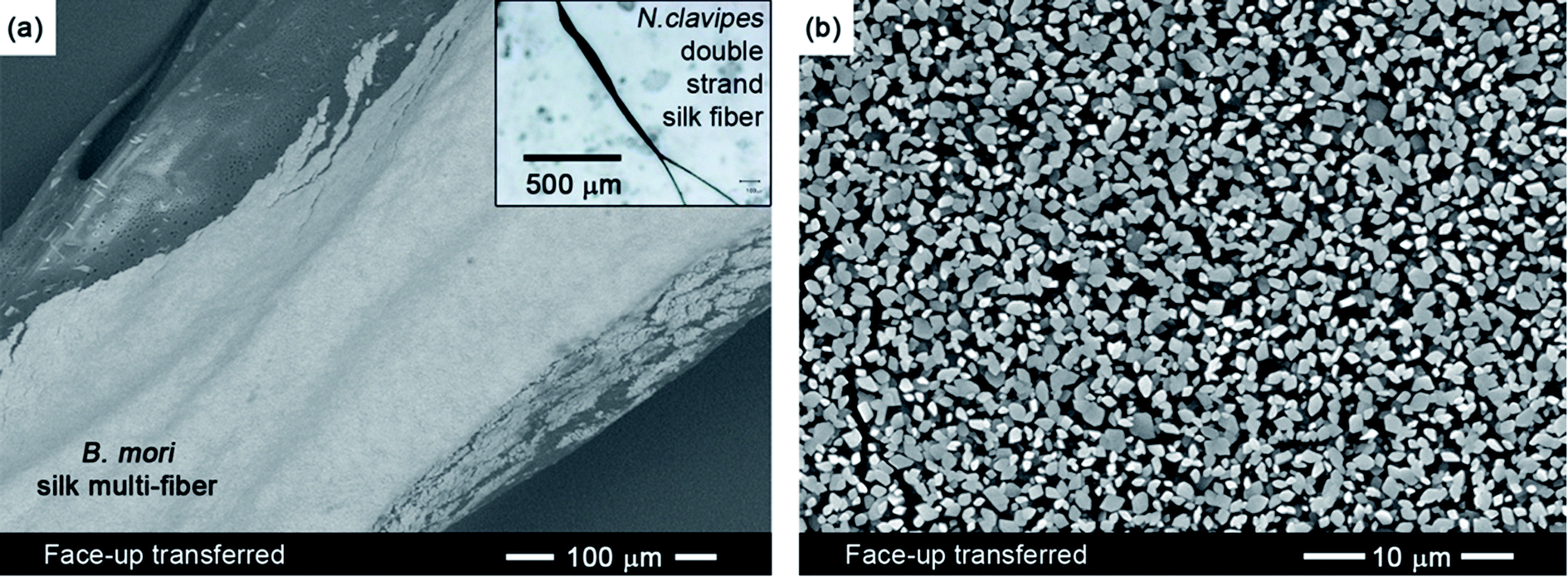 | ||
| Fig. 5 SEM images of the face-up transferred α-(BEDT-TTF)2I3 layer. (a) Low and high (b) magnification images of the face-up transferred layer on a Bombyx mori silk multi-fiber. SEM images were acquired using a scanning electron microscope (SEM) HITACHI S-3000N on a Hitachi S-570 system operating at 10 kV. The inset in (a) corresponds to a photograph of covered Nephila clavipes double-strand dragline silk fibers. | ||
Conclusions
In this work, we highlight the robustness of the BL film grown by the one-stage oxidative/annealing approach and when combined with the layer transfer processes we have developed, the BL film is demonstrated to be highly versatile. To the best of our knowledge this work gives the first demonstration of the capability to cover substrates, which are different in composition and geometric form, with flexible all-organic electrical strain sensing layers of molecular conductors (see ESI, Movie S2†). The layer transfer processes do not significantly change the electronic transport and electromechanical properties of the strain sensing polycrystalline layers of the (BEDT-TTF)2I3 conductors that are initially formed on parent PC substrates. In addition to various potential device applications, such as for humidity sensors and electrical current driven actuators, the sensing layer can also be used to study water diffusion processes. Our results should open the door to novel applications of organic molecular metals in sensing and other related technologies, and for thin film porous substrate materials, new ways to study complex diffusion processes where there is a coupling between the material volume and the diffusion species.Acknowledgements
Work by E.S. is supported by NSF-DMR 1005293 and 1309146. A portion of this work was performed at the National High Magnetic Field Laboratory, which is supported by NSF Cooperative Agreement no. DMR-0654118, by the State of Florida, and by the DOE. This work was supported in part by the Spanish Dirección General de Investigación (DGI) (project POMAs, CTQ2010-19501/BQU), the Generalitat de Catalunya (2009SGR00516). E.L. thanks CIBER-BBN, an initiative funded by the VI National R&D&i Plan 2008-2011, Iniciativa Ingenio 2010, Consolider Program, CIBER Actions and financed by the Instituto de Salud Carlos III with assistance from the European Regional Development Fund and V.L. acknowledges a grant FI-DGR from the Generalitat de Catalunya.Notes and references
- T. Ishiguro, K. Yamaji and G. Saito, Organic Superconductors, Springer, Heidelberg, 2nd edn, 1998 Search PubMed.
- H. Akamatu, H. Inokuchi and Y. Matsunaga, Nature, 1954, 173, 168 CrossRef.
- J. Ferraris, D. O. Cowan, V. Walatka and J. H. Perlstein, J. Am. Chem. Soc., 1973, 95, 948 CrossRef CAS.
- S. S. P. Parkin, E. M. Engler, R. R. Schumaker, R. Lagier, V. Y. Lee, J. C. Scott and R. L. Greene, Phys. Rev. Lett., 1983, 270 CrossRef CAS.
- P. M. Chaikin, J. F. Kwak, T. E. Jones, A. F. Garito and A. J. Heeger, Phys. Rev. Lett., 1973, 31, 601 CrossRef CAS.
- E. B. Yagubskii, I. F. Schegolev, V. N. Laukhin, R. P. Shibaeva, E. E. Kostyuchenko, A. G. Khomenko, Y. V. Sushko and A. V. Zvarykina, Pis'ma v ZhETF, 1984, 40, 387 CAS.
- D. Jerome, Chem. Rev., 2004, 104, 5565 CrossRef CAS PubMed.
- X. Yan, M. J. Naughton, R. V. Chamberlin, S. Y. Hsu, L. Y. Chiang, J. S. Brooks and P. M. Chaikin, Phys. Rev. B: Condens. Matter Mater. Phys., 1987, 36, 1799 CrossRef CAS.
- M. Tokumoto, H. Anzai, H. Bando, G. Saito, N. Kinoshita, K. Kajimura and T. Ishiguro, J. Phys. Soc. Jpn., 1985, 54, 869 CrossRef.
- K. Bechgaard, C. S. Jacobsen, K. Mortensen, H. J. Pedersen and N. Thorup, Solid State Commun., 1980, 33, 1119 CrossRef CAS.
- G. Saito, Organic Molecular Solids, CRC, Boca Raton, FL, USA, 1997, ch. 10 Search PubMed.
- R. P. Shibaeva and E. B. Yagubskii, Chem. Rev., 2004, 104, 5347 CrossRef CAS PubMed.
- G. Saito and Y. Yoshida, Bull. Chem. Soc. Jpn., 2007, 80, 1 CrossRef CAS.
- J. K. Jeszka and A. Tracz, Polym. Adv. Technol., 1992, 3, 139 CrossRef CAS.
- E. Laukhina, C. Rovira and J. Ulanski, Synth. Met., 2001, 21, 1407 CrossRef.
- T. Haneda, A. Tracz, G. Saito and H. Yamochi, J. Mater. Chem., 2011, 21, 1621 RSC.
- E. Laukhina, R. Pfattner, L. R. Ferreras, S. Galli, M. Mas-Torrent, N. Masciocchi, V. Laukhin, C. Rovira and J. Veciana, Adv. Mater., 2010, 22, 977 CrossRef CAS PubMed.
- V. Laukhin, I. Sanchez, A. Moya, E. Laukhina, R. Martin, F. Ussa, C. Rovira, A. Guimera, R. Villa, J. Aguilo, J.-C. Pastor and J. Veciana, Sens. Actuators, A, 2011, 170, 36 CrossRef CAS PubMed.
- L. R. Ferreras, R. Pfattner, M. Mas-Torrent, E. Laukhina, L. Lopez, V. Laukhin, C. Rovira and J. Veciana, Mater. Chem., 2011, 21, 637 RSC.
- D.-H. Kim, J. Viventi, J. J. Amsden, J. Xiao, L. Vigeland, Y.-S. Kim, J. A. Blanco, B. Panilaitis, E. S. Frechette, D. Contreras, D. L. Kaplan, F. G. Omenetto, Y. Huang, K.-C. Hwang, M. R. Zakin, B. Litt and J. A. Rogers, Nat. Mater., 2010, 9, 511 CrossRef CAS PubMed.
- S.-W. Hwang, H. Tao, D.-H. Kim, H. Cheng, J.-K. Song, E. Rill, M. A. Brenckle, B. Panilaitis, S. M. Won, Y.-S. Kim, Y. M. Song, K. J. Yu, A. Ameen, R. Li, Y. Su, M. Yang, D. L. Kaplan, M. R. Zakin, M. J. Slepian, Y. Huang, F. G. Omenetto and J. A. Rogers, Science, 2012, 337, 1640 CrossRef CAS PubMed.
- D. N. Rockwood, R. C. Preda, T. Yucel, X. Wang, M. L. Lovett and D. L. Kaplan, Nat. Protoc., 2011, 6, 1612 CrossRef CAS PubMed.
- Q. Lu, X. Hu, X. Wang, J. A. Kluge, S. Lu, P. Cebe and D. L. Kaplan, Acta Biomater., 2010, 6, 1380 CrossRef CAS PubMed.
- J. T. Alfrey, E. F. Gurnee and W. G. Lloyd, J. Polym. Sci., Part B: Polym. Lett., 1966, 12, 249 Search PubMed.
- Y. J. Weitsman, Composites, Part A, 2006, 37, 617 CrossRef PubMed.
- M. H. Shirangi, X. J. Fan and B. Michel, in Micro- and Opto-Electronic Materials, Structures, and Systems, ed. X. J. Fan and E. Suhir, Springer US, 2010, p. 29 Search PubMed.
- Z. Ahmad, M. P. Ansell and D. Smedley, IOP Conf. Ser.: Mater. Sci. Eng., 2011, 17, 012011 CrossRef.
- H. G. Carter and K. G. Kibler, J. Compos. Mater., 1978, 12, 118 CrossRef PubMed.
Footnote |
| † Electronic supplementary information (ESI) available: Images of formation of BEDT-TTF crystals on Bombyx mori silk, photos of different preparation stages for both face-down and face-up; as well as electronic and electromechanical properties of (BEDT-TTF)2I3-covered paper and set-up of humidity experiments and obtained data, and two movies demonstrating silk/β-(BEDT-TTF)2I3 electric current-driven actuator and deformation sensitivity test using a flexible pipette. See DOI: 10.1039/c4mh00074a |
| This journal is © The Royal Society of Chemistry 2014 |