Polymer memristor for information storage and neuromorphic applications
Yu
Chen
*ac,
Gang
Liu
*b,
Cheng
Wang
a,
Wenbin
Zhang
b,
Run-Wei
Li
*b and
Luxing
Wang
a
aKey Lab for Advanced Materials, Institute of Applied Chemistry, East China University of Science and Technology, 130 Meilong Road, Shanghai 200237, China. E-mail: chentangyu@yahoo.com
bKey Laboratory of Magnetic Materials and Devices, Ningbo Institute of Materials Technology and Engineering, Chinese Academy of Sciences, 1219 West Zhongguan Road, Ningbo, Zhejiang 315201, China. E-mail: liug@nimte.ac.cn; runweili@nimte.ac.cn
cThe State Key Laboratory of ASIC & System, Fudan University, 220 Handan Road, Shanghai 200433, China
First published on 2nd June 2014
Abstract
Polymer materials have been considered as promising candidates for the implementation of memristor devices due to their low-cost, easy solution processability, mechanical flexibility and ductibility, tunable electronic performance through innovative molecular design cum synthesis strategy and compatibility with complementary metal oxide semiconductor (CMOS) technology as well. The digital-type polymer memristor behaves as resistive random access memory with non-volatility, high density, more speed, low power consumption, large ON/OFF ratio, high endurance and long retention, and is recognized as an appealing candidate for the next generation “universal memory”. As a logic component, the analog-type memristor, with the ability to emulate the fundamental synaptic functions of short-term/long-term plasticity (STP/LTP), spike-timing dependent-plasticity (STDP), spike-rate dependent plasticity (SRDP) and “learning-experience” behaviors, can be used to construct artificial neural networks for neuromorphic computation. In this review, we shall attempt to summarize the recent progress in research on the materials, switching characteristics and mechanism aspects of two terminal polymer memristors, for both information storage and neuromorphic applications that inspire great interest in the industrial and academic communities.
 Yu Chen | Yu Chen is a full professor of East China University of Science and Technology in Shanghai. He received his Ph.D. in Organic Chemistry at Fudan University in 1996. In 2000, he joined Prof. Michael Hanack's group at the University of Tuebingen as an Alexander von Humboldt research fellow. At the end of October 2002, he moved to the University of Washington, and worked with Prof. Alex K.Y. Jen as a research associate. He has published more than 160 papers, reviews and communications in international peer-review journals. His current work mainly concerns polymeric functional materials for optoelectronics and photonics. |
 Gang Liu | Gang Liu is currently an Associate Professor at the Ningbo Institute of Materials Technology and Engineering (NIMTE), CAS. After receiving his Ph.D. degree from the National University of Singapore in 2010, he worked as a research associate at the Nanyang Technological University and then as a research fellow at the National University of Singapore from January 2010 to August 2012. In August 2012, he joined the CAS Key Laboratory of Magnetic Materials and Devices of NIMTE. His research interests include the design, preparation and engineering of polymer-based nanocomposite materials, as well as their applications in electronics and optoelectronics. |
 Cheng Wang | Cheng Wang was born in Zhejiang, China in 1988 and received his B.S. degree from the School of Chemistry and Molecular Engineering, East China University of Science and Technology in 2011. He then joined Prof. Dr Yu Chen's group as a Ph.D. student. To date he has published 10 papers in international journals. His current work concerns the design and synthesis of polymer functional materials for polymer memoristors. |
 Wenbin Zhang | Wenbin Zhang received his bachelor degree in Materials Chemistry from the Xi'an University of Technology (China) in July 2011. Since then, he has been a master student at the Ningbo Institute of Materials Technology and Engineering (NIMTE), CAS. His research interests include the design and synthesis of memristive polymers and nanocomposite materials for information storage and neuromorphic computation applications. |
 Run-Wei Li | Run-Wei Li is currently a full professor and the deputy director at the Ningbo Institute of Materials Technology and Engineering (NIMTE), the Chinese Academy of Sciences (CAS). After receiving his Ph.D. degree from the Institute of Physics (CAS) in July 2002, he worked as a JSPS research fellow at the Osaka University. In September 2003, he moved to the Kaiserslautern University as an Alexander von Humboldt research fellow. Since March 2008, he has been “One Hundred Talents” professor of CAS. His research work is mainly focused on the functional materials and devices for new types of storage and sensors. |
 Luxing Wang | Luxin Wang, born in Jiangsu, China in 1989, studied Materials Chemistry at the East China University of Science and Technology (ECUST) and received his B.S. degree from ECUST in 2012. He then joined Prof. Dr Yu Chen's group as a Ph.D. student. So far he has published several articles in international peer-review journals. His present work is mainly focused on the design and synthesis of electroactive functional materials for polymer memory devices. |
1 Introduction
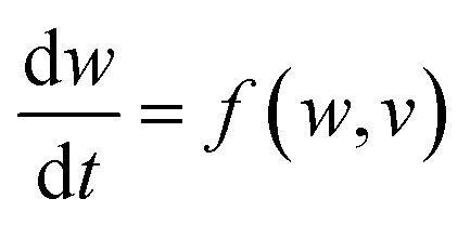
With symmetry arguments of the six mathematical relations that correlate four fundamental circuit variables of electric current i, voltage v, charge q and magnetic flux φ, Leon Chua in 1971 reasoned that there should exist the fourth basic circuit element beyond the long-known resistor, capacitor and inductor to complement the functional relation between the charge and the flux, dφ = Mdq (Fig. 1).1,2 He named the circuit element the memristor, which is short for the memory-resistor, with M representing the memristance. Briefly, the behavior of a memristor is defined by the following equations:| I = G(w,v)v | (1) |
 | (2) |
 | ||
| Fig. 1 Fundamental passive circuit elements of the resistor, capacitor, inductor and memristor and the correlations between the circuit variables. | ||
Experimentally, a memristor should be composed of an insulator sandwiched between a pair of conducting electrodes. However, none of the practical systems was found to demonstrate suitable physical properties that bridged the gap between the theoretical inception and the material realization at that moment. More importantly, with the rapid development of transistor based integrated circuits over the past forty years, researchers were less willing to pay equal attention to this newly predicted gadget. This situation lasted for almost half a century. Then, the game changed quietly in the early 2000s, when the semiconductor community began to realize that the state-of-the-art memory technology faced the monstrous crisis of the difficulties in hyper-resolution fabrication, electrostatic control and power management in the ten-nanometer regime.3,4 More efforts have been devoted to designing and developing novel device concepts and architectures to prolong the pleasant scene that the semiconductor industry has been enjoying for decades.5,6 In 2008, scientists at the HP Lab announced the first physical implementation of the memristor made from titanium oxide.7 They demonstrated that by coupling the electric field-induced ion drift and solid-state electronic transport in nanoscale devices, i–v anomalies of switching and hysteretic characteristics, multiple conductance states and negative differential resistance can be achieved and well-understood. Since then, plenty of work has been performed to investigate the memristive behavior of inorganic materials.8–13
The original definition of the memristor was further extended by Leon Chua in 2011, when he argued that regardless of the device materials and physical operating mechanisms, all two-terminal systems that present a frequency-dependent, pinched hysteretic loop confined to the first and third quadrants of the v–i plane are memristors.14–16 With this broadened definition, it is immediately realized that the distinctive “fingerprint” of the memristive system has been to a great extent observed and documented for over two centuries prior to the HP nanoscale demonstration in 2008.17–20
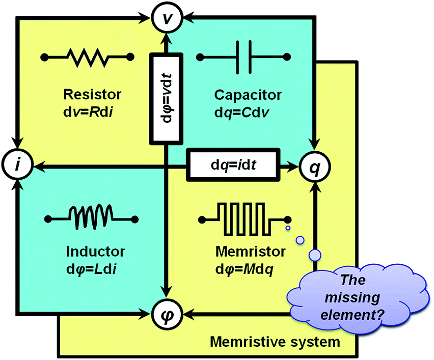
One particular example of the memristor is the resistive random access memory (RRAM) with digital-type (or abrupt) current switching and large ON/OFF ratio characteristics (Fig. 2a).21–26 Generally, the size of a single RRAM cell can be down-scaled to a few tens of nanometers,27 while the cross-point array structure and the three-dimensional stacking capability, in which the memory cells have an area of about 4F2 (F is the minimum feature size of the device), enable the fabrication of high-density devices.28–30 Nevertheless, the resistive switching occurs in a few nanoseconds,31,32 which promises fast writing, reading and erasing during operation. With the benefits of non-volatility, high density, more speed, low power consumption, high endurance, long retention, good down-scaling capability, three-dimensional stacking ability and compatibility with complementary metal oxide semiconductor technology,11,33–36 resistive random access memory provides several key performance characteristics that exceed conventional transistor based data storage technology, and is recognized as an appealing candidate for the next generation “universal memory”.4
 | ||
| Fig. 2 i–v characteristics of memristors showing (a) digital-type (abrupt) and (b) analog-type (incremental) conductance switching behaviors. The inset of (a) shows a metal/insulator/metal sandwich structure. The inset of (b) shows a schematic illustration of biological synapse. | ||
On the other hand, memristors with analog-type switching behavior, which are characterized by continuous and incremental change of device resistance or conductance with a relatively lower ON/OFF ratio, trigger recent research campaign in synaptic mimicking and neuromorphic computing (Fig. 2b).37–42 Artificial neural networks with the synaptic density approaching 1010 synapses per cm2 and high biomimicking inter-neuron connectivities have been constructed from crossbar memristor structures, demonstrating not only the fundamental synaptic functions of short-term/long-term plasticity (STP/LTP), spike-timing dependent-plasticity (STDP), spike-rate dependent plasticity (SRDP) and “learning-experience” behavior on the device level, but also the cooperation and interaction behaviors of multiple synapses on the network level.43,44 With such memristor based neuromorphic systems, the conventional von Neumann computers may be ultimately revolutionized to perform the judging, decision-making and learning actions that are intrinsic to mammalian species.
In comparison to metal oxides, chalcogenides, amorphous silicon and other inorganic counterparts, polymer materials exhibit attractive features of low-cost potential, easy processability, mechanical flexibility and ductibility, as well as the tunable electronic performance through a molecular design cum synthesis strategy.23–25 In particular, the solution processing capability of polymer materials allows them to be handled via dip coating, blade casting, spray coating, spin coating, roller-coating and even ink-jet printing, making the more elaborated processes of vacuum deposition of functional thin films eliminatable. Extensive studies have been conducted on the investigation of conductance/resistance switching, electrical hysteresis, memory and memristive effects in polymer and polymer-based composite materials, toward the development of novel polymer functional materials and device structures for memory performance optimization and neuromorphic mimicking.45–54 In this review, we will summarize the recent research progress on the material preparation, switching characteristic and mechanism aspects of two terminal polymer memristors, for both information storage and neuromorphic applications that inspire great interest in the industrial and academic communities.
2 Polymer resistive random access memory materials and mechanisms
Individual or package of molecules are capable of conducting and switching electrical currents, as well as storing electrical bits of information.55 Instead of encoding “0” and “1” as the amounts of charge stored in a silicon-based cell, polymer resistive random access memory (polymer memory for short) stores information in a different manner, for instance, based on the low and high conductance in response to an external electric field.23–26 The conductance states can be read nondestructively and do not require power supply to maintain a given state. As such, the severe problems of charge leaking in the state-of-the-art flash memory devices that are faced by the Si-based technologies during the downscaling competition can be well solved, and the polymer memories are considered as leading candidates for future information storage applications.56,57Since electrical conductivity is the product of charge carrier concentration and mobility, changes in either the carrier concentration or mobility, or both, can lead to changes in the material or device conductance states. In polymer memories, the conductance bistability may arise from changes in the intrinsic properties of the switching media, and several switching mechanisms, including charge transfer, phase change, conformation change and reduction-oxidation (redox) interactions have been proposed.45 Due to the lack of advanced characterizing and analyzing tools, less direct physical evidences are available to support the above mentioned models. Thus, identifying the operation mechanism is still difficult at the moment, which hinders the further development of the functional materials and improvement in the device performance (in particular the endurance and reliability of the switching devices).21 Nevertheless, well-established conduction mechanisms including Ohmic conduction, Schottky emission, thermionic emission, space-charge-limited current, tunneling current, ionic conduction, hopping conduction and others have been adopted to account for charge transport in each conductance state.
2.1 Blends or mixtures of memory polymer materials
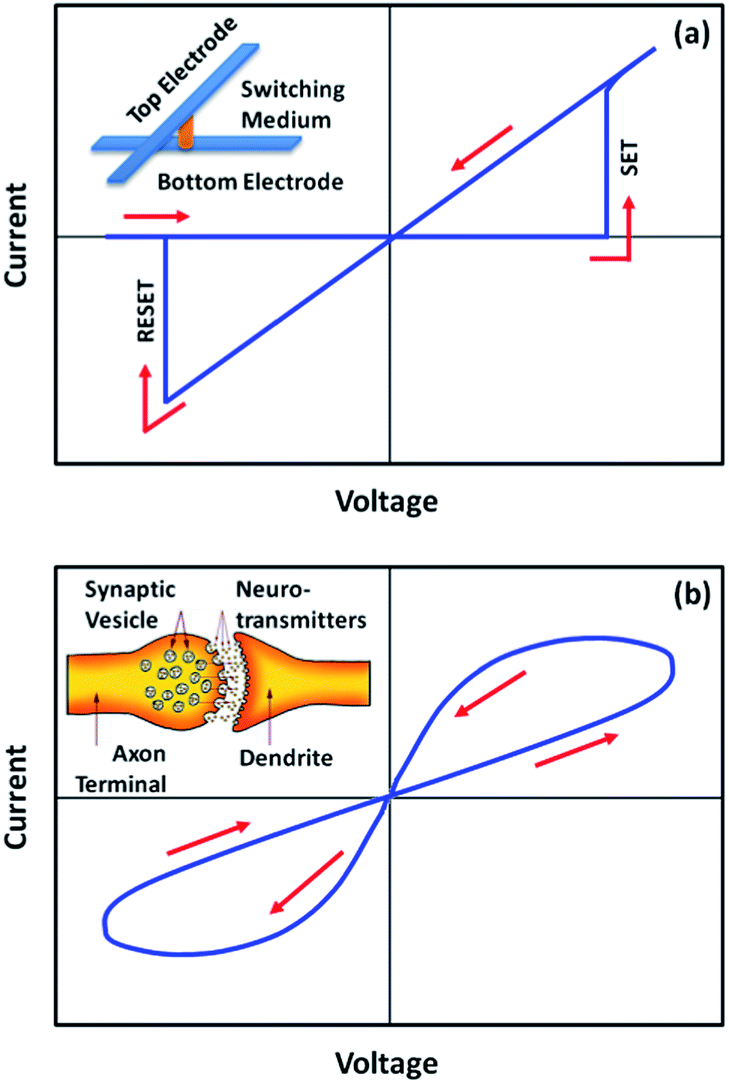
Various polymer materials, in the form of blends or mixtures,57–68 matrices for nanoparticles or inorganic compounds,69–90 single-component active materials,91–145 polymer–C60/polymer–graphene nanocomplexes,146–160 and even biomacromolecules,161–164 have been explored for memory applications with low switching voltage, large ON/OFF state current ratio, long retention time and high endurance capabilities.In the pioneering studies of polymer memories, blends or mixtures of polymers, in which both or all the constituting components are electroactive, are often used as the switching media. For instance, Forrest et al. spun a layer of polyethylene dioxythiophene:polystyrene sulfonic acid (PEDOT:PSS) onto the surface of a Si p–i–n thin film diode that was predeposited onto a stainless steel substrate (Fig. 3).57,58 When a sufficiently high current density was applied through the electrode/PEDOT:PSS/Si/electrode structure, the device can be permanently open-circuited, with the device conductivity decreased by five to six orders of magnitudes. Facilitated by the X-ray photoelectron spectroscopy and temperature induced conductivity measurements, it was found that the application of large current would cause the re-distribution of PEDOT+:PSS− segments in the polymer layer, leading to an aggregation of the insulating PSS− chains near the electrode/polymer interface. Such a morphology not only prevented charge injection from the cathode into the nearby conducting PEDOT+:PSS− grains, but also blocked the conducting pathway between grains. This large irreversible reduction in conductivity and large conductivity contrast ratio (ON/OFF ratio) allows the polymer/semiconductor junction to function as a write-once-read-many-times (WORM) memory element, which is promising for the fast, permanent, large-scale and ultralow-cost archival storage of massive digital images.
 | ||
| Fig. 3 (a) Schematic illustration of the WORM memory and the chemical structure of PEDT:PSS. (b) Sulfur 2P spectra at the cathode/polymer interface for a n-Si/PEDT:PSS/Au heterojunction device before (solid line) and after (dashed line) switching from the conductive to insulating state. Insets show the current-driven morphological change that causes the conductivity switching. (c) i–v characteristics of the PEDT:PSS based memory pixel showing conductivity switching behavior. Reproduced with permission from ref. 57 and 58. | ||
Pal and Bandyopadhyay studied the effect of a supramolecular matrix on the switching property of Rose Bengal (RB) molecules.59 Initially, the electron-acceptor moieties presented in Rose Bengal perturbed the conjugation of the dye molecule, leading to a high resistance of the device. When a negative bias was applied, electrons were injected into the film, neutralizing the deactivating groups and restoring the conjugation of Rose Bengal. Consequently, a highly conducting state was obtained in the device with the ON/OFF ratio of ∼104. When the voltage was subsequently swept positively, electrons were removed from the Rose Bengal molecules, breaking the conjugation of each molecule and switching the device to the poorly conducting state. When electrostatic self-assembly (ESA) films consisting of RB anions and poly(allylamine hydrochloride) (PAH) cations were used as the switching media, the ON state current was comparable to that of the spin-cast RB film, while the OFF state current was 1–3 orders of magnitude higher, which in turn resulted in a much lower ON/OFF ratio. In the ESA-based device, the lone pair of electrons on the free amino groups of PAH could release the twisted stress of the RB molecule and restore the conjugation to some extent, leading to the observed increase in the OFF state current.
Lu et al. also blended polymers with organic dyes to explore the memory behavior.60 Upon mixing the AB-type block copolymer of PStCH-b-P4VP containing pendant electron-donating 3-(4-(diethylamino) phenyl)-1-(4-(4-vinylbenzyloxy) phenyl) prop-2-en-1-one (StCH) and 4-vinylpyridine (4VP) moieties with the organic dye of tetra(4-carboxylphenyl) porphyrin (TCPP), strong charge transfer interactions between the P4VP blocks and TCPP molecules were established. Tuning the loading ratio of TCPP in the PStCH-b-P4VP matrix could modulate the interaction between the P4VP and TCPP components, which in turn influenced the electrical behavior of the composite significantly (Fig. 4). Composites with 0%, 1% and 3% of TCPP in the PStCH-b-P4VP matrix behaved as WORM, dynamic random access memory (DRAM) and DRAM memories, respectively. It was also found that the OFF states of devices containing 0% and 1% TCPP were both dominated by Pool–Frenkel emission, while that for the 3% TCPP-containing device was controlled by space-charge-limited current. On the other hand, all three devices showed Ohmic conduction behavior in the ON state. With more acceptor content in the composites, the 3% TCPP device also exhibited a lower switching voltage in comparison to that of the 1% TCPP device, suggesting that the memory characteristics can be well modulated by the charge transfer interaction between the electron donor and acceptor groups. Similar demonstration was also provided by Liu and Chen, when they mixed triphenylamine (TPA)-based polyimide (PI) with coronene or diimide derivative PDI-DO.61 Flexible memory devices with DRAM, Flash and WORM switching characteristics were realized on the poly(ethylene naphthalate) substrate.
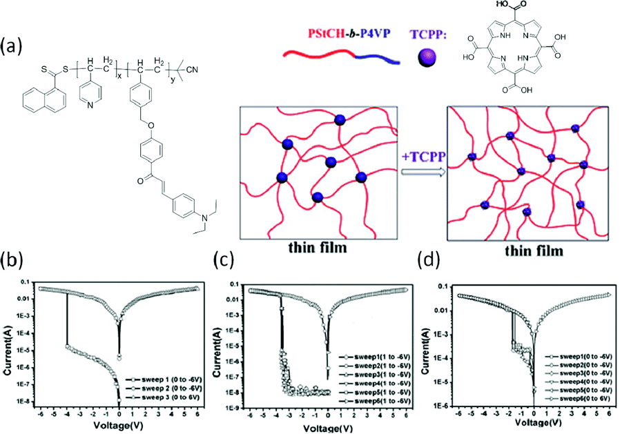 | ||
| Fig. 4 Chemical structure of PStCH-b-P4VP and TCPP and an illustration of their composite (a) and i–v characteristics of PStCH-b-P4VP memory devices containing (b) 0%, (c) 1% and (d) 3% TCPP contents, respectively. Reproduced with permission from ref. 60. | ||
Carbon-based nanomaterials also form interactive memory composites with polymer materials.62 The composition and aggregated domain size of the filled additives are key parameters to tune their memory characteristics. Chen et al. reported the fabrication of polymer memory with blends of [6,6]-phenyl-C61-butyric acid methyl ester (PCBM) and conjugated rod-coil poly[2,7-(9,9-dihexylfluorene)]-block-poly-(2-vinylpyridine) diblock copolymers (PF-b-P2VP).63 The use of conjugated rod-coil copolymers provides an essential platform for the formation of the self-organized nanostructure, with the π–π interaction between the conjugated rods acting as an additional factor to control the thin film morphology and device properties. It was demonstrated that static random access memory (SRAM) behavior with an ON/OFF ratio of 107 was achieved in devices containing only PF10-b-P2VP37 or PF10-b-P2VP68 polymers. Shallow charge traps of the block copolymer and rapid back transfer were employed to explain the volatile nature of the pure polymer devices. Though the P2VP segments were less efficient to trap charge carriers, increase in the P2VP content nevertheless delayed the back transfer of trapped carriers, leading to a longer retention time of the ON state in the PF10-b-P2VP68 device. When PCBM was introduced into the polymer films, electric-field induced charge transfer interaction occurred between the polymer and PCBM components, and WORM memory behaviors were observed in both the PF10-b-P2VP37 and PF10-b-P2VP68 devices. Further increase in the PCBM content resulted in a percolated pathway for charge carrier transport, and led to conductor behavior in the composite devices. The influence of the block length ratio of block copolymers or PCBM composition provided an easy approach to tune the memory characteristics of the solution-processable data storage nano-materials.64–67
The operation parameters of polymer memory devices usually suffer from severe fluctuations, which lead to consequently false programming and error readout limitations that hinder their practical applications. Therefore, obtaining reproducible and uniformly distributed switching parameters is always a big challenge for the polymer memory communities. Li et al. designed a very smart strategy to overcome this problem by controlling the resistance of the polymer device gradually and exactly via manipulating the doping level of a toluenesulfonic acid (TsOH):poly(schiff base) (PA) system (Fig. 5).68 It was found that the Pt/PA–TsOH/Pt devices exhibited smooth, self-rectifying i–v characteristics during the resistive switching process, with a rectifying ratio of 10–100, an ON/OFF ratio of 600 and a small dispersive index of less than 5% for both the switching voltage and the ON/OFF ratio in over 1200 switching cycles. The promising uniformity of the PA–TsOH system is superior to those reported RRAM devices, suggesting that the controllable protonic doping is an effective way to optimize the uniformity of resistive switching behaviors. Using protonic acids with larger molecular weights and sizes can further increase the self-rectifying property of poly(schiff base), as well as enhance the device retention capability of the doped system. Nevertheless, by using different reset voltages and compliance current levels, multilevel storage was established during the consecutive modulation of the device resistance, which is extremely important for increasing the data storage capacity exponentially.
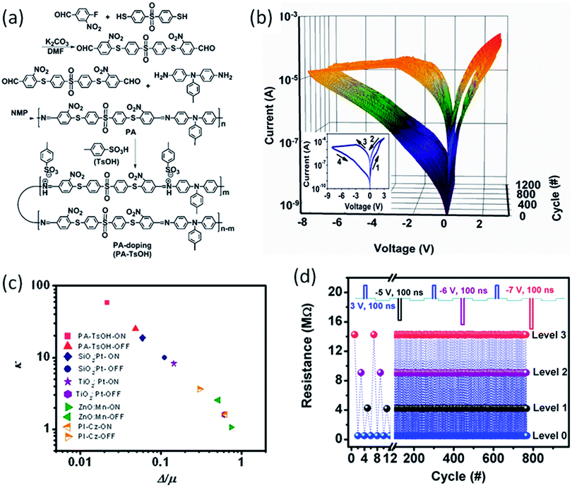 | ||
| Fig. 5 (a) Synthesis route of the monomer and poly(schiff base). (b) i–v characteristics of the PA–TsOH system. The inset of (b) is the first I–V cycle of the Pt/PA–TsOH/Pt devices. (c) Plots of the Weibull exponent (k) as a function of the standard deviation to mean ratio (Δ/μ) for the switching parameters of the Pt/PA–TsOH/Pt devices (red) and the reported devices (navy, purple, olive, orange). (d) Multilevel operation of the Pt/PA–TsOH/Pt devices in a pulse mode. The inset of (d) illustrates the voltage pulse utilized for the device programming. The reading voltage is −0.5 V. Reproduced with permission from ref. 68. | ||
2.2 Polymer matrices for nanoparticles and inorganic compounds
Other than interacting with the guest components, the polymer materials also form an inert matrix for the nanoparticles, carbon nanomaterials and inorganic compounds.69 Yang et al. fabricated a memory device with polystyrene (PS) as the inert matrix and gold nanoparticles (Au–DT) and 8-hydroxyquinoline (8HQ) as the switching materials.70,71 It was demonstrated that the pristine device was in a low conductivity state and underwent an abrupt transition to a high conductivity state under an external bias with an ON/OFF ratio of ∼104 (Fig. 6). The application of a negative bias could reprogram the device back to the low conductivity state. Since the OFF–ON transition occurred in less than 25 ns, which was much faster than the occurrence of any electrochemical rearrangement, conformational change or isomerization, the conductance switching might originate from an electric field-induced electronic process. Through the i–v curve fitting, optical spectroscopic and atomic force microscopic measurements, it was confirmed that the electric-field-induced charge transfer between the Au–DT and 8HQ, and the subsequent charge tunneling among the latter, were responsible for the high conductivity state after transition. Other than serving as the matrix for metal nanoparticle and nanowire dispersion,72–74 the polymers containing hetero atoms also act as chelating agents to drag metal species from the chemically active electrode into the organic layer to form particulated conductive filaments.75,76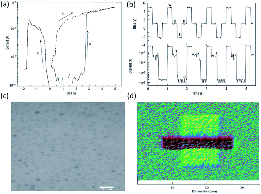 | ||
| Fig. 6 (a) i–v characteristics and (b) write–read–erase cycles of the Al/PS + Au–DT + 8HQ/Al devices, (c) transmission electron micrograph of the gold nanoparticles, (d) the scanning surface potential AFM image of the Au–DT + 8HQ + PS film with Al as the bottom electrode and silicon wafer as the substrate. Reproduced with permission from ref. 70. | ||
The unique physicochemical and morphological properties of carbon nanotubes (CNTs) have made them promising materials for application in electronics and optoelectronics.77 Liu and Kang et al. prepared Al/PVK–CNT/ITO sandwiched structures.78 By varying the CNT content in poly(N-vinylcarbazole) (PVK) composite thin films, the electrical conductance of the sandwiched structure could be tuned in a controlled manner (Fig. 7). Distinctly different electrical conductance behaviors, such as (i) insulator, (ii) bistable memory and (iii) conductor, were discernible from the i–v characteristics. The turn-on voltage of the bistable devices decreased with the increase in CNT content of the composite film. Both the WORM and rewritable devices were stable under a constant voltage stress or a continuous pulse voltage stress, with an ON/OFF state current ratio of more than 103. Furthermore, the CNT content-dependent while temperature-independent electrical bistabilities observed in the Cu or Au top electrode device clearly ruled out the possibility of the interfacial effect or filamentary conduction in the PVK–CNT memory systems. Through i–v modeling and theoretical estimation, charge trapping/detrapping in CNT has been proposed to account for the electrical bistability.
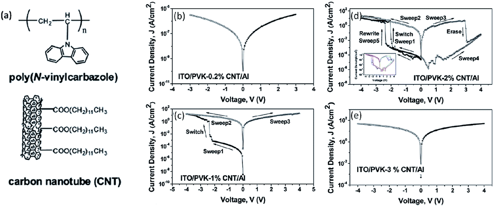 | ||
| Fig. 7 Chemical structures of PVK and CNT (a), and i–v characteristics of Al/PVK–CNT/ITO devices containing 0.2% (b), 1% (c), 2% (d) and 3% (e) carbon nanotube content. Reproduced with permission from ref. 78. | ||
In comparison to its allotropes of fullerene and carbon nanotube, pseudo two-dimensional graphene exhibits fascinating properties of quantum electronic transport, tunable bandgap, high charge carrier mobility, excellent mechanical elasticity and strength, and others.25 The crystalline carbon nanosheets also serve as charging and discharging media in flexible non-volatile bistable memories.79 Kim et al. have sandwiched graphene nanosheets between insulating poly(methyl methacrylate) (PMMA) polymer layers to construct memory devices. With the presence of graphene charge-storage media in the as-fabricated devices, the i–v characteristics of the Al/PMMA/graphene/PMMA/ITO/PET structure showed a room temperature conductance bistability and a non-volatile memory effect (Fig. 8). The ON/OFF ratio of the devices was larger than 1 × 10⁷, which could be reproduced in a single cell for 1.5 × 10⁵ cycles or retained for over 24 h. No interference was observed when the devices dimension was scaling down by 50%, nor bended into curves with a surface curvature radius of 10 mm.
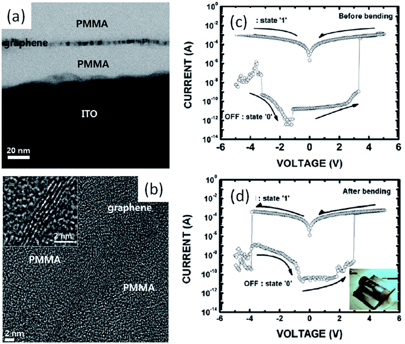 | ||
| Fig. 8 Cross-sectional (a) TEM and (b) HRTEM images of the PMMA/graphene/PMMA structure; i–v characteristics of the Al/PMMA/graphene/PMMA/ITO/PET devices (c) before and (d) after bending. Reproduced with permission from ref. 79. | ||
Further, the polymer–carbon nanomaterial composites have been integrated into flexible devices, one diode–one resistor (1D1R) arrays and a three dimensional matrix to demonstrate promising practical implementation of the polymer memories.80–84 For instance, the composite of insulating PI and semiconducting PCBM was used as the switching medium to construct the polymer memory on poly(ethylene terephthalate) (PET) flexible substrates.81–83 The switching voltage, ON/OFF ratio, endurance and retention capability were well maintained when the devices were bended to various degrees, indicating the stability of the memories under stresses. Nevertheless, the combination of the Al/p-type Si Schottky diode and PI:PCBM resistive switching unit greatly improved the sensing efficiency of the memory arrays, leading to the possibility of high-density integrated polymer memories (Fig. 9).82 Then the same group demonstrated a conceptual design of 3D-stacked 8 × 8 crossbar polymer memory with PI:PCBM composites as the switching media.84 Individual memory cells in different layers can be independently written, read and erased with excellent memory performance in terms of ON/OFF ratio, endurance and retention capability.
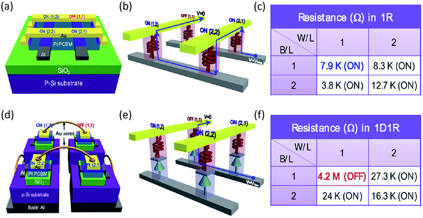 | ||
| Fig. 9 Schematic illustration of (a) the device structure, (b) cross-talk interference during reading the (1,1) OFF cell with neighboring (1,2), (2,1) and (2,2) ON cells, (c) resistance values of each cell of a 1R polymer memory array of 2 × 2 cells, (d) the device structure, (e) current flow during reading the (1,1) OFF cell with neighboring (1,2), (2,1) and (2,2) ON cells and (f) resistance values of each cell of a 1D1R polymer memory array of 2 × 2 cells. Reproduced with permission from ref. 82. | ||
Polymer materials also serve as the matrix for inorganic compound nanoparticles.85,86 Lee et al. blended titanium dioxide nanoparticles (TiO2 NPs) with PVK and fabricated an 8 × 8 array structured device.87 The embedment of TiO2 NPs into the PVK thin film resulted in bistable resistance states and a unipolar non-volatile memory effect. By varying the concentration of TiO2 NPs, the ON/OFF ratio of the devices were significantly modulated, where the PVK–TiO2 volume ratio of 150![[thin space (1/6-em)]](https://www.rsc.org/images/entities/char_2009.gif) :1 gave a much lower thermally-activated OFF state current and the highest ON/OFF ratio over 105. Arrhenius temperature-dependent electrical measurements indicated that in the temperature range of 150 to 300 K, filamentary conduction and tunneling transport accounted for the ON state of the ITO/PVK–TiO2 NPs (volume ratio of 150:1)/Al device, while thermal dissolution of the conductive filaments by the high current in the resetting process accounted for the unipolar nature of the memory effect.
:1 gave a much lower thermally-activated OFF state current and the highest ON/OFF ratio over 105. Arrhenius temperature-dependent electrical measurements indicated that in the temperature range of 150 to 300 K, filamentary conduction and tunneling transport accounted for the ON state of the ITO/PVK–TiO2 NPs (volume ratio of 150:1)/Al device, while thermal dissolution of the conductive filaments by the high current in the resetting process accounted for the unipolar nature of the memory effect.
Molybdenum disulfide (MoS2) is another 2D nanomaterial used for novel electronics and optoelectronics.88 The intrinsic bandgap, high mobility and large specific surface area allow MoS2 to compete with graphene in high performance field-effect transistors, gas sensors, light emitting diodes, lithium ion batteries and others.89 The unique energy level and quantum confinement effect also render MoS2 as charge trapping units for memory applications. Huang and Zhang et al. used poly(vinylpyrrolidone) (PVP) to enhance the mass exfoliation of MoS2 from its layered bulk material, and incorporated the PVP-coated MoS2 composite (MoS2–PVP) into flexible memories (Fig. 10).90 The device with a configuration RGO (reduced graphene oxide)/MoS2–PVP/Al exhibited a non-volatile rewritable memory effect arising from the charge trapping/detrapping behavior of MoS2 in the PVP dielectric matrix.
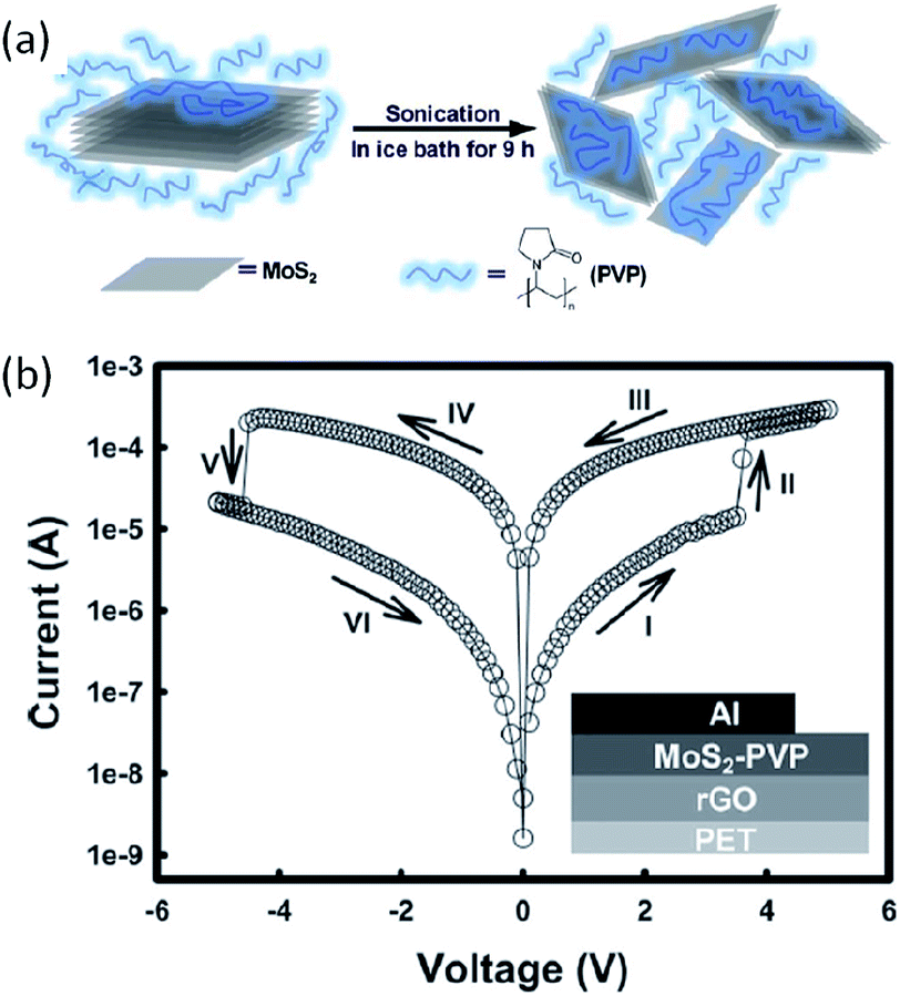 | ||
| Fig. 10 (a) Schematic illustration of polymer-assisted exfoliation of MoS2, and (b) i–v characteristics of the rGO/MoS2–PVP/Al flexible memory device. Inset shows the schematic diagram of the memory device structure. Reproduced with permission from ref. 90. | ||
2.3 Single-component polymer active materials
Doping or mixing of polymers with guest components provides an easy approach to fine-tune the electrical properties and therefore the memory performance of bistable devices. However, it may not always give rise to uniformly dispersed and compatible components, and thus may result in phase separation and ion aggregation, which are unfavorable to the device performance. To avoid such problems, much attention have been paid to processable memory polymer materials, which can provide the required electronic properties within a single macromolecule, while still process good chemical, mechanical and morphological characteristics.23–26The extensive study of current–voltage–electroluminescence characteristics of conjugated polymers indicates that the space and trapped charges play an important role in the electrical performance of the electronic and optoelectronic devices.91–93 Pal et al. in 2002 used poly[3-(6-methoxyhexyl)thiophene] (P6OMe), which was capable of retaining space charges, to construct non-volatile data storage devices.94 It was found that the memory performance was directly related to the relaxation dynamics of the accumulated space charges.95,96 Depending on amplitude of the applied voltages, hysteresis has been observed in the i–v characteristics with different densities of charges stored at the metal/polymer interfaces. By varying the delay between two applied voltage pulses, during which the space charges were relaxed or redistributed, the stored charges were proved to dominate the charge injection from the electrode and hence the device current. The slow relaxation process has resulted in the conductance states that could be retained for more than 1 h, or refreshed/erased at will.
Ling and Kang et al. prepared a conjugated copolymer (PFOxPy, Fig. 11) containing both electron-donor and -acceptor groups.97 Interestingly, the Al/PFOxPy/ITO structured device showed volatile memory behavior, with the ON state electrically sustainable by a refreshing voltage pulse. When a reverse pulse was used, the device could also be reset to the initial OFF state, and thus behaved as a DRAM device. Fairly good reliability and performance of the PFOxPy DRAM device has been demonstrated, with a high ON/OFF current ratio of up to 106, excellent endurance of both the ON and OFF states for up to 108 read cycles at a read voltage of 1.0 V, and retention capability for more than 10 h. Molecular simulation of the molecular orbitals of the basic unit (BU), which includes all the functional moieties and segments of PFOxPy, showed that PFOxPy is a p-type material and holes dominate the conduction process. The continuous positive electrostatic potential (ESP) surface provided a charge carrier migration channel along the conjugated backbone, while the negative ESP region served as a trap to block the transport. Since the depth of the traps is shallow, the filled traps could easily be detrapped, leading to the low write/erase voltages and volatility of PFOxPy based devices.
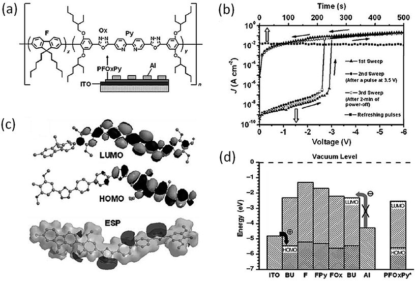 | ||
| Fig. 11 (a) Chemical structure of PFOxPy, (b) i–v characteristics of the Al/PFOxPy/ITO device, (c) simulated LUMO, HOMO, and ESP surfaces of the BU of PFOxPy, and (d) LUMO and HOMO energy levels for the basic unit (BU) and functional segments of PFOxPy along with the work function of the electrodes. The energy levels of the copolymer measured by cyclic voltammetry are indicated with an asterisk. Reproduced with permission from ref. 97. | ||
Instead of being placed in the conjugated backbone of the polymer alternatively or randomly, the electron-donor and acceptor groups can also been tethered to the end of the polymer backbone or to the pendants.98 For instance, devices based on a covalently bridged conjugated Disperse Red 1–poly[9,9-bis(4-diphenylaminophenyl)-2,7-fluorene]–Disperse Red 1 (DR1–PDPAF–DR1) triad exhibited electrical bistability in the i–v characteristics with the rewritable nature, an ON/OFF ratio of up to 103, good endurance (108 cycles) and retention (104 s) capability (Fig. 12).99 The DR1 acceptor can also be connected to the pendant carbazole units of PVK to give the DR1-functionalized PVK copolymer (PVDR).100 Nanoaggregated PVDR displayed helical columnar stacks with large grain sizes, which benefited the occurrence and stabilization of the intermolecular charge hopping process. As a result, Al/PVDR/ITO devices constructed from the pre-assembled solution of PVDR showed improved WORM memory performance with much greater stability than that of the non-nanoaggregated PVDR devices (Fig. 13).
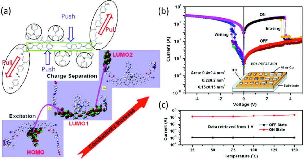 | ||
| Fig. 12 (a) Chemical structure of DR1–PDPAF–DR1 and plausible excitation and charge separation processes simulated with DFT theory, (b) i–v characteristics of the Al/DR1–PDPAF–DR1/ITO device, and (c) temperature-independent ON and OFF state currents of the Al/DR1–PDPAF–DR1/ITO device. Reproduced with permission from ref. 99. | ||
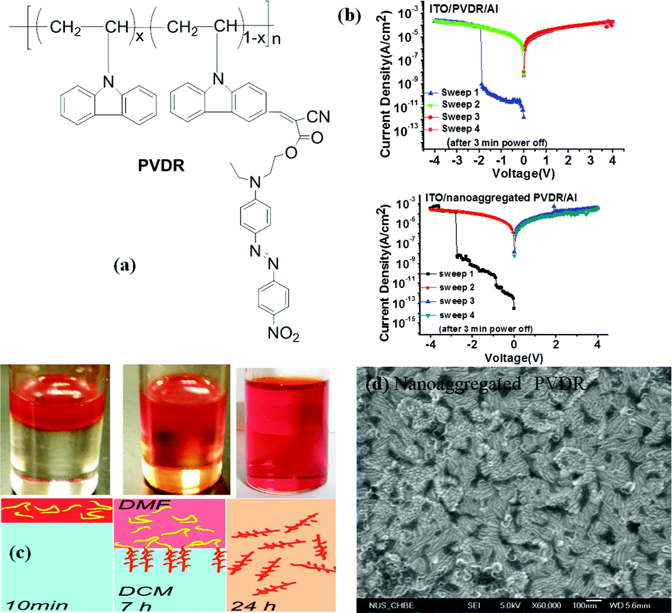 | ||
| Fig. 13 (a) Chemical structure of PVDR, (b) i–v characteristics of the Al/PVDR/ITO and Al/nanoaggregated PVDR/ITO devices, (c) schematic illustration of the interfacial self-assembly process of PVDR. The top red layer is PVDR dissolved in DMF, and the bottom layer is DCM. The volume/volume ratio of these two solvents was 1/10, and (d) the HRSEM image of the surface morphology of the spin-coated nanoaggregated PVDR film on the ITO substrate. Reproduced with permission from ref. 100. | ||
The use of azobenzene moieties as the spacers between electron donor and acceptor groups in the pendant chains of vinyl based polymers was extensively investigated by Kang, Chen and Lu et al.101–107 Polymers with electron accepting terminal moieties (–Br or –NO2) in the pendant azobenzene exhibited WORM memory behavior, while those with electron-donating terminal moieties (–OCH3) showed rewritable memory behavior.101 Moreover, the switching threshold voltages of the device varied almost linearly with the D–A pair content in the copolymer.102 When stronger electron acceptors (2CN) were used, an even higher ON/OFF ratio could be obtained in the WORM device (Fig. 14).103,104 Optical absorption spectroscopic and X-ray photoelectron measurements, high-resolution transmission electron microscopy imaging, and the density functional theory calculations of the polymer films at both the ON and OFF states indicated that the observed electrical bistability could be attributed to the field-induced charge-transfer interaction between the carbazole electron-donor unit and the terminal electron-acceptor unit, and subsequent charge trapping at the intermediate azobenzene chromophores.104,107
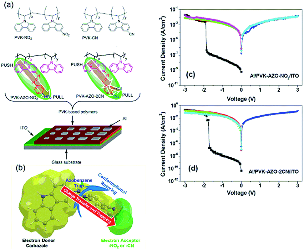 | ||
| Fig. 14 (a) Chemical structure of the AZO based polymers, (b) schematic diagram of the electronic transition and conformational reconfiguration of the AZO based polymers, and i–v characteristics of (c) the Al/PVK–AZO–NO2/ITO and (d) Al/PVK–AZO–2CN devices. Reproduced with permission from ref. 103. | ||
By introducing the transition-metal complex into the backbone or pendants, the optoelectronic and electronic properties of functional polymers can be easily tuned.108–111 Choi et al. inserted the redox active ferrocene into the conjugated backbone of PFT2 randomly.110 The copolymer exhibited two reversible peaks at 0.58 eV and 0.97 eV, respectively, which were assigned to the oxidation of ferrocene and the bithiophene conjugated backbone of PFT2–Fc. When fabricated into Al/LiF/PFT2–Fc/ITO devices, rewritable memory behavior with a set/reset voltage of −1.9 V/+1.4 V, an ON/OFF ratio of 103, an endurance of more than 100 cycles and a retention time longer than 7 h were achieved.
Huang and Zhao et al. systematically investigated the memory characteristics of phosphorescent Ir(III) complexes-containing iamPx series polymers.112–115 For instance, in iamP1–iamP3 the cationic Ir(III) complexes were placed in the main-chain of the conjugated copolymer for non-volatile rewritable memory exploration. The Al/iamPx/ITO devices exhibited low reading, writing and erasing voltages of −1.6 V, 2.8 V and −1.0 V, respectively, as well as a high ON/OFF ratio of more than 105 that can be sustained for up to 104 s or 108 read cycles. Such promising memory characteristics have been ascribed to the polarized charge-transfer state between 9,9′-dioctylfluorene moieties and cationic Ir(III) complex moieties.
Conformational reconfiguration may also lead to conductance switching in carbazole based polymers. Kang and Lim et al. explored the memory performance of two carbazole-containing polymers with different spacer units.116 Fluorescence spectroscopic measurements indicated that the carbazole pendants would rotate along the spacer axis to form partial face-to-face excimer configuration under electrical stimulation, which favored intra-/intermolecular charge hopping between adjacent pendants with overlapped orbitals. As a result, the device based on poly(2-(N-carbazolyl)ethylmethacrylate) (PMCz) with a shorter space unit exhibited WORM memory behavior with an ON/OFF current ratio up to 106, while the device based on poly(9-(2-((4-vinylbenzyl)oxy)ethyl)-9H-carbazole) (PVBCz) with a longer space unit exhibited volatile memory behavior with an ON/OFF current ratio of approximately 103 (Fig. 15). With the absence of a spacer unit between the pendant carbazole group and the vinyl backbone, regioregular PVK exhibited only one conductivity state (ON state), therefore suggesting that the inherent difference in the degree of regioregularity and the ease of conformational relaxation of the field-induced regioregular carbazole groups should be the primary origin of the differences in memory behavior among the three carbazole-containing polymers.117–119
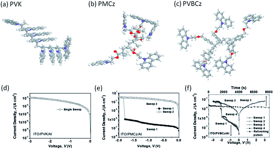 | ||
| Fig. 15 Optimized molecular geometry and the i–v characteristics of (a and d) PVK, (b and e) PMCz and (c and f) PVBCz. Reproduced with permission from ref. 116. | ||
Triphenylamine (TPA)-containing polymers are also demonstrated to exhibit promising electronic and optoelectronic properties.120–126 For instance, flexible dual functional devices with multi-colored electrochromic and volatile memory characteristics have been fabricated from a solution-processable electroactive TPA-containing polyimide (Fig. 16).123,124 The incorporation of the electron-donating, packing-disruptive starburst TPA moiety with the methoxyl group at the para-position of phenyl groups not only enhances the thermal stability and solubility of the polymer, but also helps to lower the oxidation potential associated with increasing electrochemical stability and multi-stage EC characteristic. Consequently, the polymer device showed electrochromism with high contrast ratio, high coloration efficiency, low switching time, and the outstanding stability for long-term electrochromic operation in both visible and near-infrared regions.
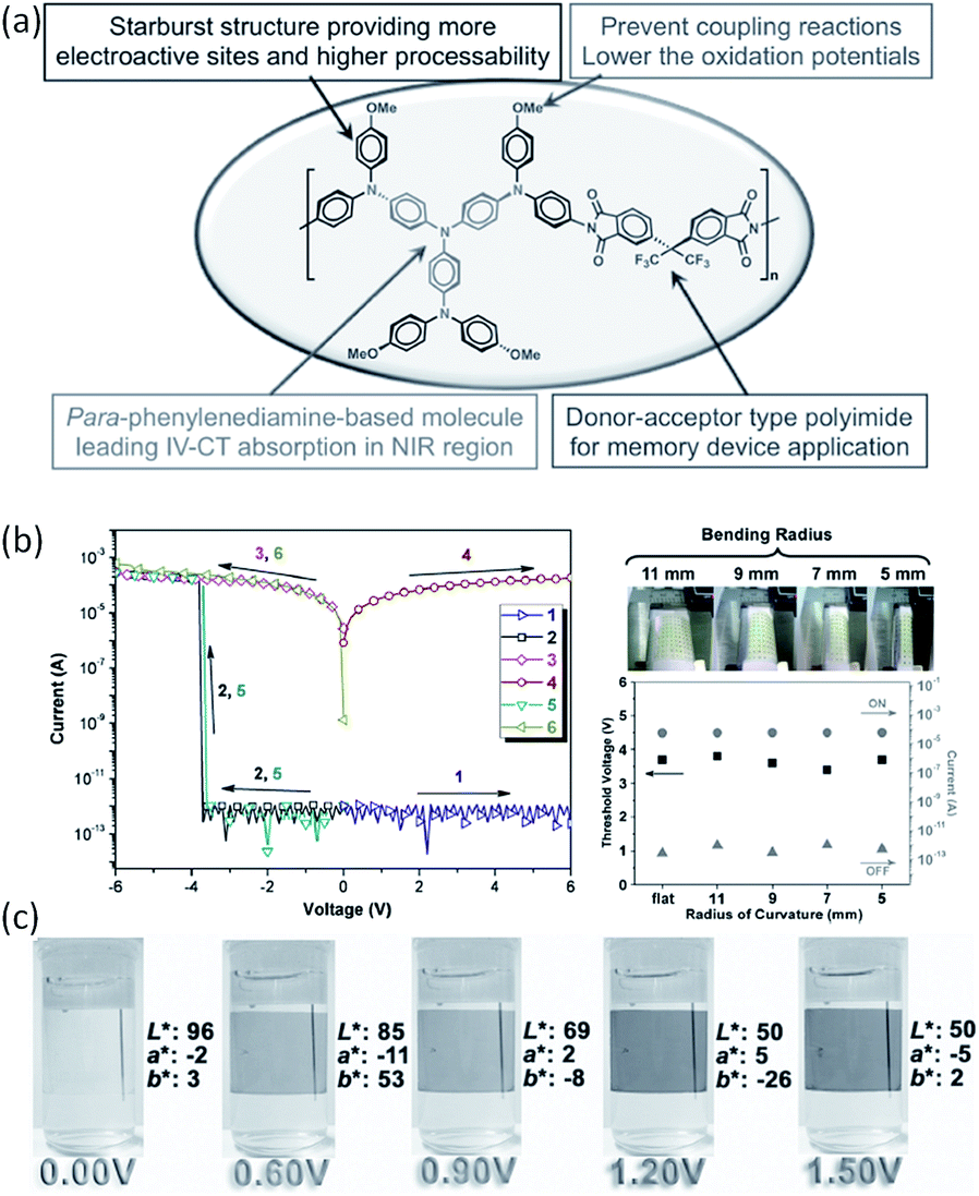 | ||
| Fig. 16 (a) Design strategy, (b) i–v characteristics and (c) electrochromic performance of a starburst triphenylamine-based polyimide. Reproduced with permission from ref. 124. | ||
Polyimides, as mentioned previously, are promising candidates for electronic applications owing to their excellent thermal and structural stability.127,128 Plenty of efforts have been devoted in developing high-performance memory polyimides since 2006.129–137 For example, Ree et al. synthesized a carbazole-containing polyimide (6F-HAB-CBZ PI) and fabricated an electrically programmable non-volatile memory device.130 The PI film demonstrated interesting and excellent unipolar switching behaviors, where the pristine OFF state device can be set to the ON state by applying a positive or a negative bias with a current compliance preset of a low level, and then switched off by applying a positive or a negative bias with a current compliance preset of a higher level. Again, the Joule heating effect with higher resetting current accounted for the unipolar switching behavior.
In the pioneering approaches using doped or mixed polymeric systems for memory applications, the occurrence of aggregation of nanoparticles or irregular phase separation originating from the poor compatibility between polymers and nanoparticles or small molecules usually caused non-uniform dispersion and thus poor reproducibility of device performance.138 To achieve homogeneous dispersion of electroactive components and controlled electrical properties, both random and block copolymers with controlled molecular weight distribution, well-defined nanostructure and morphology have been developed.139–145 Lee et al. synthesized block copolymers of poly(9-(4-vinylphenyl)carbazole)-b-poly(2-vinylpyridine) (PVPCz-b-P2VP) containing both electron donating carbazole (PVPVz) and accepting pyridine (P2P) blocks (Fig. 17).142 By adjusting the PVPCz:P2VP block ratios, various morphologies from spheres to lamellar, as well as different electrical behaviors from metallic conductors, switching memory and insulators, have been reproducibly demonstrated. Devices based on the lamellar structured polymer showed an ON/OFF ratio of 103 over long duration or with stable endurance.
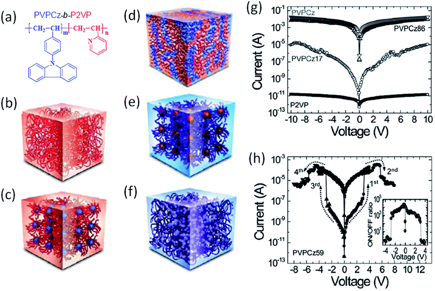 | ||
| Fig. 17 (a) Chemical structure, (b–f) schematic nanostructure illustrations and (g and h) i–v characteristics of block copolymers of PVPCz-b-P2VP with different PVPCz:P2VP ratios. Reproduced with permission from ref. 142. | ||
2.4 Polymer–fullerene and polymer–graphene nano-complexes
As mentioned above, carbon nanomaterials have been widely used in polymer memory applications.25,62,77 To avoid the uniform aggregation of the phase separation issue in fullerene (C60)–polymer composites, Ling and Ree et al. directly attached the electron accepting fullerene moieties to the pendants of the electron donating polymer (Fig. 18).146,147 The covalent tethering of C60 to PVK lead to good solubility of the nanocomplex in a wide range of organic solvents. When sandwiched between Al and ITO electrodes, the as-fabricated Al/PVK–C60/ITO structure behaved as non-volatile rewritable memory with an ON/OFF ratio of more than 105, write/erase voltages around −2.8 V/+3.0 V, a retention time over 12 h and 108 endurance cycles under ambient conditions.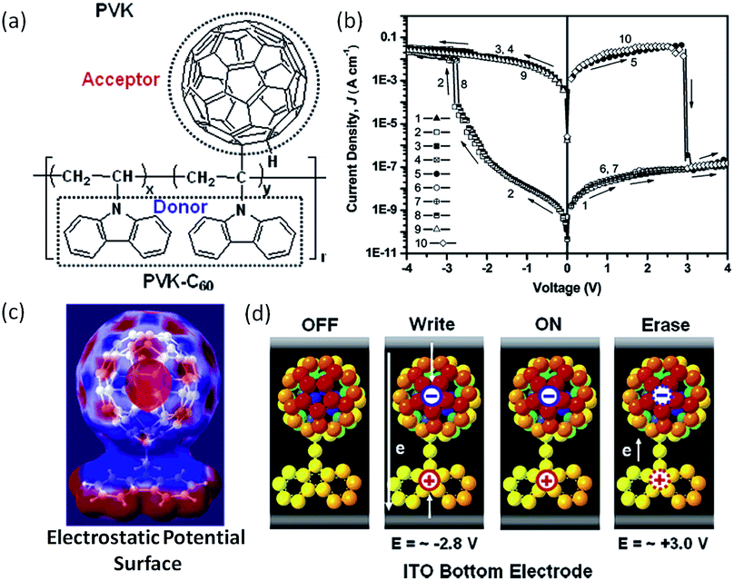 | ||
| Fig. 18 (a) Chemical structure, (b) i–v characteristics, (c) simulated electrostatic potential surface and (d) switching mechanism of PVK–C60. Reproduced with permission from ref. 146. | ||
Similar to the fullerene allotrope, chemical functionalization also plays a key role in tailoring the structure, processability, and electronic properties of graphene nanosheets.148–151 By using the “grafting to” or “grafting from” method, a variety of polymers have been covalently incorporated onto the surface as well as the edge of GO nanosheets.152–154 Chen and Kang et al. firstly grafted PVK with GO nanosheets for the fabrication of an Al/PVK–GO/ITO sandwich structure (Fig. 19).148,149 A significant bandgap of ∼2 eV was generated in the PVK–GO complex through charge transfer interaction between the PVK donor and GO acceptor moieties. With this bandgap, the PVK–GO nanocomplex was made switchable between two conductance states with excellent accuracy. Triphenylamine (TPA)-based conjugated polymer was also grafted to GO to form a resistance switchable TPAPAM–GO nanocomplex.149 It was proposed that the field-induced injection of electrons from the peripheral molecules of PVK or TPA to the central GO plane could reduce the insulating GO nanosheet to the more conductive RGO with less charge carriers scattering and enhanced in-plane transport, therefore switching the virgin low conductive device to the high conductive state. The electronic transition process was reversible, and the application of a high enough voltage with opposite polarity could induce reverse transfer of electrons, and reduced the conductivity back to its initial value.
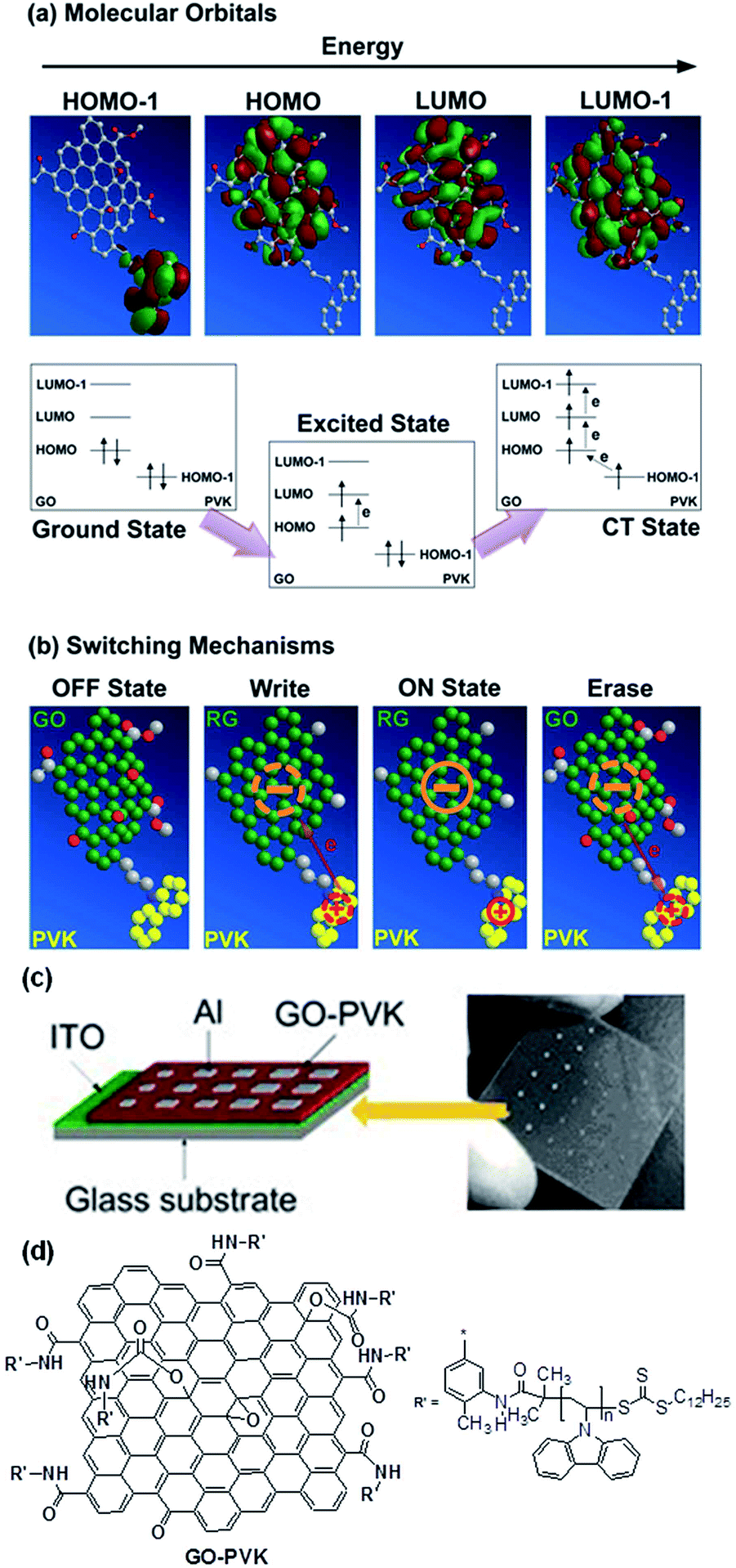 | ||
| Fig. 19 (a) Molecular orbitals and electric field-induced electronic processes from the ground state to the charge transfer state, (b) plausible switching mechanism of GO–PVK. The schematic 3D chemical structure of GO–PVK is simplified for better understanding of the electronic process in the molecule, (c) memory device structure and (d) molecular structure of GO–PVK. Reproduced with permission from ref. 148. | ||
With the recovered crystalline quality and electronic structures, RGO was also functionalized with electroactive polymers through similar routes, albeit that the covalent attachment occurred only at the RGO laminate edges. For instance, 1,3-dipolar cycloaddition reaction of azomethine ylides was adopted directly to functionalize the RGO nanosheets.155–160 The reaction between sarcosine, RGO and poly-[{4,4′-(9H-fluorene-9,9-diyl)bis(N,N-diphenyl benzene amine)}{4-(9H-carbazol-9-yl)benzaldehyde}(9,9-dihexyl-9H-fluorene)] (PFCF–CHO) led to a highly soluble conjugated polymer-grafted RGO (PFCF–RGO).158 Non-volatile rewritable memory effects were demonstrated in the sandwich structure of Al/PFCF–RGO/ITO, with the switching voltage of around −1.2 V and the ON/OFF ratio over 104, outperforming the memory devices based on polymer-grafted GO nanosheets.
2.5 Electroactive biomacromolecules and nanocomposites
Recently, nano-structured biomaterials have also been explored to bridge nanoscale electrical circuits with nanoscale electronic devices.161–164 Yang et al. in 2006 reported the fabrication of a memory device using tobacco mosaic virus (TMV) conjugated with platinum nanoparticles (TMV–Pt, Fig. 20).163,164 The TMV is a positive-sense single-stranded RNA plant virus composed of 2, 130 identical coat proteins and placed in Group IV under the Baltimore classification system for viruses. Generally, the rigid virion is a 300 nm-long tube with 18 nm outer and 4 nm inner diameters. The wild-type TMV-U1 was chosen as the template for nano-structure synthesis because the platinum ions could be bonded to the specific functional groups on the protein surface of the virus to form uniformly distributed nanoparticles. The resultant TMV–Pt composite exhibited unique conductance switching behavior and acted as the first demonstrated bio-memory device. The device can be turned on and off at 3.1 and 22.4 V, respectively, with an ON/OFF ratio of ∼103. The controlled sample without TMV did not exhibit any switching behavior, indicating that the virus was crucial for the construction of bio-memory devices.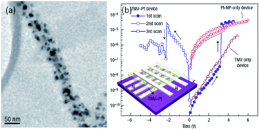 | ||
| Fig. 20 (a) Transmission electron microscopic image and (b) i–v characteristics of the TMV–Pt system. Reproduced with permission from ref. 163. | ||
3 Polymer synaptic biomimicking materials and mechanisms
Neuromorphic computing that could emulate the brain function is an attractive computation paradigm to complement the von Neumann computer system achieved with the state-of-the-art CMOS technology.165 Synapse is the cellular unit for learning and memory, while artificial synapses are considered as the fundamental components to construct neuromorphic circuits.166,167 On the other hand, the nonlinear transmission characteristics and the self-adaptive nature of the analog-type memristors provide them essential capability toward synaptic mimicking and neuromorphic computing.40Bandyopadhyay and Higuchi et al. in 2011 introduced the concept of polymer memristor for the first time, by replicating the potential distribution of the dopant–titania complex with a metal–organic hybrid polymer (CP), in which a metal ion was directly bonded to an organic ligand (Fig. 21).47 The i–v characteristics of a Au–CP–Au lateral structure traced in the voltage range of ±5 V showed current jumping from the initial low level to a high level at −5 V, as well as another jump from the high level to the initial level at +5 V. The bistable switching behavior exhibited a typical “pinch-off” feature of a memristive device, and could be operated at different voltage levels with different current responses, therefore providing multilevel storage capability to replace the existing binary computing devices.
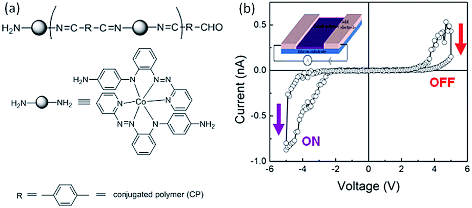 | ||
| Fig. 21 (a) Chemical structure and (b) i–v characteristics of the metal–organic hybrid polymer (CP). Reproduced with permission from ref. 47. | ||
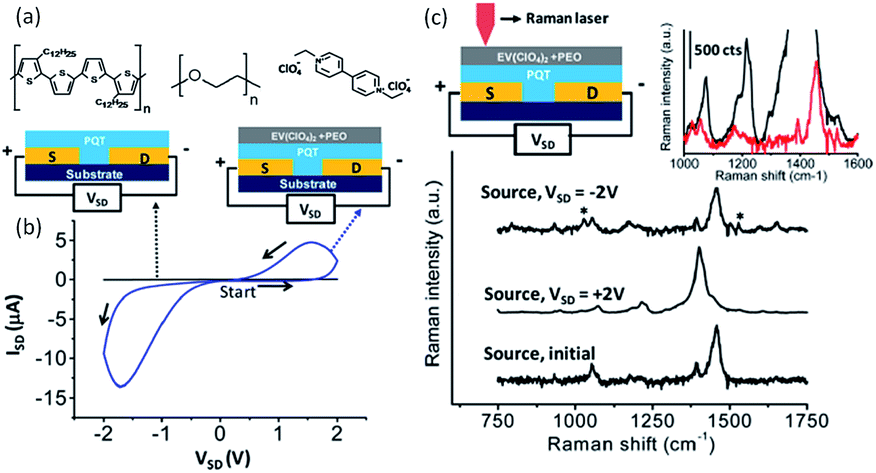
McCreery et al. used polythiophene as the electroactive component and ethylviologen perchlorate as the redox counter-electrode materials to build both polymer memristors (Fig. 22).50,51 The conductivity of the device could be reversibly switched between high and low conductance states with a “write/erase” (W/E) bias, while read with the same or a separate readout circuit. In situ and spatially resolved Raman spectroscopic measurements revealed that reversible oxidation of polythiophene to its polaron form, which was accompanied and stabilized by the one-electron reduction of viologen species, accounted for the observed incremental switching of the device conductance. Such spectroscopic evidence of the concurrent redox reactions of both polythiophene and viologen in solid-state devices correlated electrochemical redox reactions with the device conductance switching, and provided essential guidance for further improvements in device performance.
 | ||
| Fig. 22 (a) Chemical structure of polythiophene, polyethyloxide and ethylviologen perchlorate, (b) i–v characteristics of the two- and three-terminal devices made from polythiophene, polyethyloxide and ethylviologen perchlorate, and (c) schematic illustration of the in situ Raman spectroscopic measurements, as well as the spectra obtained before and after conductance switching. Reproduced with permission from ref. 51. | ||
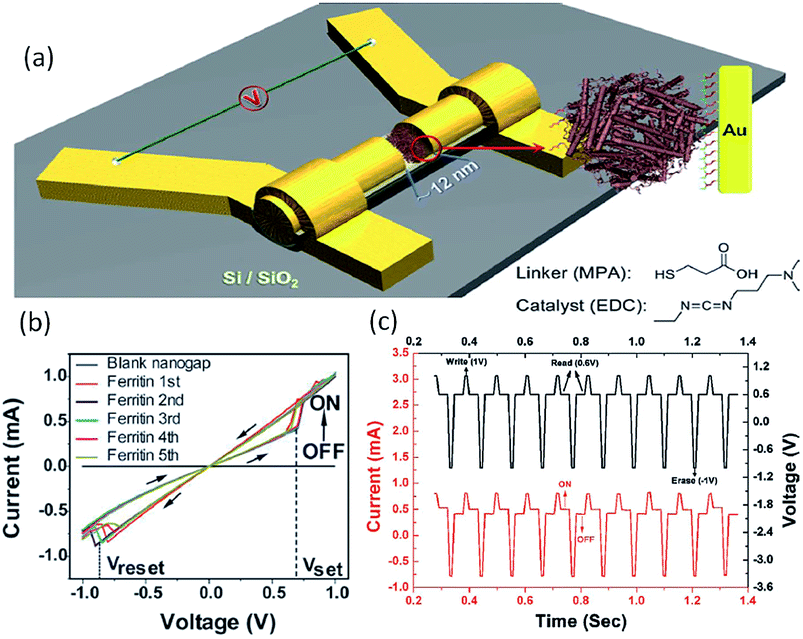
Biomacromolecules have also been explored for potential logic applications. For instance, Chen et al. exploited natural ferritin and an on-wire lithography (OWL) technique to fabricate protein-based nano memristors.52,53 Ferritin was chosen as the electroactive biomaterial because it is the major intracellular ion storage protein with reversible electrochemical redox activity.168,169 The i–v characteristics of a two terminal device with the 12 nm nanogap without the inclusion of ferritin exhibited no conductance within the noise limit of the measurement (Fig. 23). When ferritin was immobilized into the nanogap, reversibly programmable resistance switching was observed. The device could be set and reset with voltages of +0.7 V/−0.8 V, respectively, which was the biomolecular analog of the titanium dioxide thin film devices. By controlling the amount of ferritin introduced into the nanogap, the device conductance was further modulated in both the ON and OFF states. Nevertheless, although the write–read–erase cyclic operations were also shown, the ability to process digital information within a single cell, in addition to the data storage function, was not demonstrated in the ferritin-, nor CP-/polythiophene-based devices.
 | ||
| Fig. 23 (a) Schematic illustration, (b) i–v characteristics and (c) of write–read–erase operations the ferritin-based nanogap devices. Reproduced with permission from ref. 52. | ||
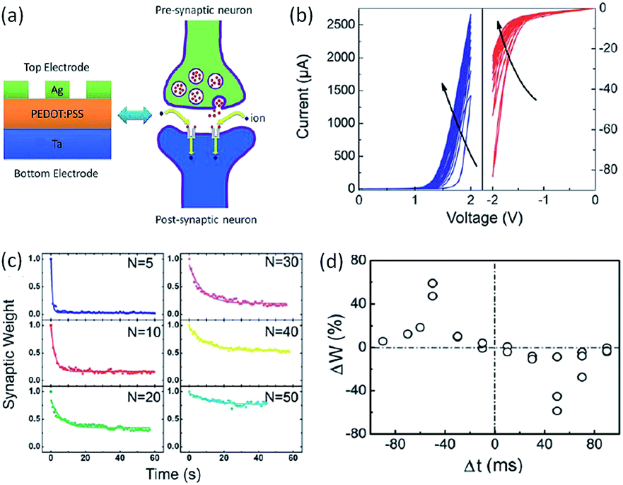
The capability of mimicking bio-synapse was first evaluated in polymer systems by Zeng and Pan in 2013.54,170–172 They fabricated the polymer memristor with the simple structure of Ag/poly(3,4-ethylenedioxythiophene):poly(styrenesulphonate) (PEDOT:PSS)/Ta. Essential synaptic plasticity and learning behaviors, including short-term plasticity, long-term plasticity, spike-timing dependent plasticity and spike-rate-dependent plasticity, have been emulated (Fig. 24). When the Ag/PEDOT:PSS/Ta memristor was scanned consecutively with positive voltages from 0 V to 2 V, the current value increased incrementally. When the device was scanned continuously from 0 V to −2 V, the current value decreased with the number of scans. The continuous adjustment of the device conductivity well mimicked the modulation of synaptic weight by consecutive spikes in a biological synapse.166 The rectification effect observed in the system enabled the emulation of single direction information transmission in biological synapses and neurons. Upon removing the applied voltage stimulation, the current dropped fast at the beginning, then gradually decayed, and finally stabilized to an intermediate value. As the numbers of the electrical stimulus increased, the relaxation time of the current decay increased correspondingly, mimicking the short-term plasticity (STP) to long-term plasticity (LTP) transition in biological systems. When the device was stimulated again, only a few stimuli were able to recover the initial memory level, suggesting that the information can be recalled easily after it has been forgotten. Through transmission electron microscopic and energy-dispersive X-ray spectroscopic analysis, it was demonstrated that the movement of the Ag interface by redox reaction of the active TE, as well as the elastic effect of the polymer matrix, accounted for the conductance switching, memory and learning processes of the Ag/PEDOT:PSS/Ta memristor.
 | ||
| Fig. 24 (a) Schematic illustration, (b) the i–v curve with nonlinear transmission characteristics, (c) STP-to-LTP transition and (d) STDP behavior of a Ag/PEDOT:PSS/Ta memristor. Reproduced with permission from ref. 54. | ||
4 Concluding and outlook remarks
With the rapid development of information technology in recent years, digital gadgets, such as pads and smart phones, have become an essential part of our daily life.173 As the performance of these devices advances, their complexity increases with the concomitant shrinkage in device dimensions. However, the device shrinking campaign is not endless. Beyond certain size (for example 16 nm as the predicted threshold), silicon based devices will become less stable to store individual bits. On the “International Semiconductor Road Map”, current memory technologies are pacing towards the end of the road.4 On the other hand, the state-of-the-art von Neumann computer systems are unable to process complicated tasks of learning, judging or decision making, no matter how fast they can run. From both the technological and the economic points of view, the development of novel information storage and processing materials and devices has become an emergent issue in electronics industry.As memory, the digital-type polymer memristors or RRAM devices exhibit an ON/OFF ratio as high as 103 to 106, which promise a significantly low misreading rate of the three-dimensional memory stacking architecture.174 Moreover, power supply is not required to maintain the stored information, and the devices are non-volatile and suitable for long-term mass data storage. As logic devices, the analog-type polymer memristors are capable of mimicking the learning and memorizing function of a biological synapse. With all the above mentioned and other advantages of mechanical flexibility, high data storage capacity and large-scale connectivity through three-dimensional stacking, over the current state-of-the-art memories and other upcoming technologies, the polymer memristor promises itself great potential as an alternative, or at least a supplement, to silicon for the next generation information technology applications.
Despite considerable advances in fundamental research on the polymer memristor during the last decade, it is still in the infancy and obstacles persist against the commercially viable devices. The underlying switching and conduction mechanisms in polymer memristors have yet to be clearly understood. Relationships among the electrical transition phenomena, device parameters (including programming/erasing voltage and speed, ON/OFF ratio, retention time, reprogramming ability and cyclability), material structures, and chemicophysical properties should also be explored to understand the solid-state physics and electronics. In spite of the great challenges faced by it at the moment, the polymer memristor proves to be one of the most promising electronic technologies of the 21st century.
Acknowledgements
The authors are grateful for the financial support of the National Natural Science Foundation of China (51333002, 21074034, 51303194, 61328402), Research Fund for the Doctoral Program of Higher Education of China (20120074110004), the State Key Project of Fundamental Research of China (973 Program, 2012CB933004), the Chinese Academy of Sciences, the Fundamental Research Funds for the Central Universities, the State Key Laboratory of ASIC & System of Fudan University (11KF007), Ningbo Science and Technology Innovation Team (2011B82004), Ningbo Natural Science Foundation (2013A610031) and the Shanghai Leading Talents program.Notes and references
- L. O. Chua, IEEE Trans. Circuit Theory, 1971, 18, 507–519 CrossRef.
- L. O. Chua and S. M. Kang, Proc. IEEE, 1976, 64, 209–223 CrossRef.
- K. K. Likharev, “Electronics below 10 nm” in Nano and Giga Challenges in Microelectronics, Elsevier, Amsterdam, 2003 Search PubMed.
- International Technology Roadmap for Semiconductors (ITRS), 2009, edn; http://public.itrs.net/.
- J. Chen, M. A. Reed, A. M. Rawlett and J. M. Tour, Science, 1999, 286, 1550–1552 CrossRef CAS.
- C. Joachim, J. K. Gimzewski and A. Aviram, Nature, 2000, 408, 541–548 CrossRef CAS PubMed.
- D. B. Strukov, G. S. Snider, D. R. Stewart and R. S. Williams, Nature, 2008, 453, 80–83 CrossRef CAS PubMed.
- J. J. Yang, D. B. Strukov and D. R. Stewart, Nature Nanotechnol., 2013, 8, 13–23 CrossRef CAS PubMed.
- Y. Yang and W. Lu, Nanoscale, 2013, 5, 10076–10092 RSC.
- D. H. Kwon, K. M. Kim, J. H. Jang, J. M. Jeon, M. H. Lee, G. H. Kim, X. S. Li, G. S. Park, B. Lee, S. Han, M. Kim and C. S. Hwang, Nat. Nanotechnol., 2010, 5, 148–153 CrossRef CAS PubMed.
- M. J. Lee, C. B. Lee, D. S. Lee, S. R. Lee, M. Chang, J. H. Hur, Y. B. Kim, C. J. Kim, D. H. Seo, S. Seo, U. I. Chang, I. K. Yoo and K. Kim, Nat. Mater., 2011, 10, 625–630 CrossRef CAS PubMed.
- J. Yao, L. Zhong, D. Natelson and J. M. Tour, J. Am. Chem. Soc., 2011, 133, 941–948 CrossRef CAS PubMed.
- M. Wuttig and N. Yamada, Nat. Mater., 2007, 6, 824–832 CrossRef CAS PubMed.
- L. O. Chua, Appl. Phys. A, 2011, 102, 765–783 CrossRef CAS.
- L. O. Chua, Proc. IEEE, 2012, 100, 1920–1927 CrossRef.
- T. Prodromakis, C. Toumazou and L. Chua, Nat. Mater., 2012, 11, 478–481 CrossRef CAS PubMed.
- A. Volta, Philos. Trans. R. Soc. London, 1800, 90, 403–431 CrossRef.
- H. Davy, Nicholson's Journal of Natural Philosophy, Chemistry and the Arts, 1800, 4, 326–328 Search PubMed.
- O. W. Richardson, The Emission of Electricity from Hot Bodies, Longmans, Green and Co., 1st edn, 1916, vol. 304 Search PubMed.
- H. J. Reich and W. A. Depp, J. Appl. Phys., 1938, 9, 421 CrossRef PubMed.
- D. S. Jeong, R. Thomas, R. S. Katiyar, J. F. Scott, H. Kohlstedt, A. Petraru and C. S. Hwang, Rep. Prog. Phys., 2012, 75, 076502 CrossRef PubMed.
- X. J. Zhu, J. Shang and R.-W. Li, Front. Mater. Sci., 2012, 6, 183–206 CrossRef.
- C. L. Liu and W. C. Chen, Polym. Chem., 2011, 2, 2169–2174 RSC.
- B. Cho, S. Song, Y. Ji, T. W. Kim and T. Lee, Adv. Funct. Mater., 2011, 21, 2806–2829 CrossRef CAS.
- Y. Chen, B. Zhang, G. Liu, X. D. Zhuang and E. T. Kang, Chem. Soc. Rev., 2012, 41, 4688–4707 RSC.
- W. P. Lin, S. J. Liu, T. Gong, Q. Zhao and W. Huang, Adv. Mater., 2014, 26, 570–606 CrossRef CAS PubMed.
- J. Y. Son, Y. H. Shin, H. Kim and H. M. Jang, ACS Nano, 2010, 4, 2655–2658 CrossRef CAS PubMed.
- A. Sawa, Mater. Today, 2008, 11, 28–36 CrossRef CAS.
- W. W. Zhuang, W. Pan, B. D. Ulrich, J. J. Lee, L. Stecker, A. Burmaster, D. R. Evans, S. T. Hsu, M. Tajiri, A. Shimaoka, K. Inoue, T. Naka, N. Awaya, A. Sakiyama, Y. Wang, S. Q. Liu, N. J. Wu and A. Ignatiev, Tech. Dig. – Int. Electron Devices Meet., 2002, 193–196 CAS.
- I. G. Baek, D. C. Kim, M. J. Lee, H. J. Kim, E. K. Yim, M. S. Lee, J. E. Lee, S. E. Ahn, S. Seo, J. H. Lee, J. C. Park, Y. K. Cha, S. O. Park, H. S. Kim, I. K. Yoo, U. I. Chung, J. T. Moon and B. I. Ryu, Tech. Dig. – Int. Electron Devices Meet., 2005, 750–753 Search PubMed.
- C. Yoshida, K. Tsunoda, H. Noshiro and Y. Sugiyama, Appl. Phys. Lett., 2007, 91, 223510 CrossRef PubMed.
- W. Guan, S. B. Long, Q. Liu, M. Liu and W. Wang, IEEE Electron Device Lett., 2008, 29, 434–437 CrossRef CAS.
- Q. F. Xia, W. Robinett, M. W. Cumbie, N. Banerjee, T. J. Cardinali, J. J. Yang, W. Wu, X. M. Li, W. M. Tong, D. B. Strukov, G. S. Snider, G. Medeiros-Ribeiro and R. S. Williams, Nano Lett., 2009, 9, 3640–3645 CrossRef CAS PubMed.
- V. V. Zhirnov, R. K. Cavin, III, S. Menzel, E. Linn, S. Schmelzer, D. Braeuhaus, C. Schindler and R. Waser, Proc. IEEE, 2010, 98, 2185–2200 CrossRef.
- K.-H. Kim, S. Gaba, D. Wheeler, J. M. Cruz-Albrecht, T. Hussain, N. Srinivasa and W. Lu, Nano Lett., 2012, 12, 389–395 CrossRef CAS PubMed.
- S. Yu, H.-Y. Chen, B. Gao, J. Kang and H. S. P. Wong, ACS Nano, 2013, 7, 2320–2325 CrossRef CAS PubMed.
- J. Borghetti, G. S. Snider, P. J. Kuekes, J. J. Yang, D. R. Stewart and R. S. Williams, Nature, 2010, 464, 873–876 CrossRef CAS PubMed.
- T. Ohno, T. Hasegawa, T. Tsuruoka, K. Terabe, J. K. Gimzewski and M. Aono, Nat. Mater., 2011, 10, 591–595 CrossRef CAS PubMed.
- T. Chang, S. H. Jo and W. Lu, ACS Nano, 2011, 5, 7669–7676 CrossRef CAS PubMed.
- Z. Q. Wang, H. Y. Xu, X. H. Li, H. Yu, Y. C. Liu and X. J. Zhu, Adv. Funct. Mater., 2012, 22, 2759–2765 CrossRef CAS.
- K. Kim, C. L. Chen, Q. Truong, A. M. Shen and Y. Chen, Adv. Mater., 2013, 25, 1693–1698 CrossRef CAS PubMed.
- S. Yu, B. Gao, Z. Fang, H. Yu, J. Kang and H. S. P. Wong, Adv. Mater., 2013, 25, 1774–1779 CrossRef CAS PubMed.
- Y. V. Pershin and M. Di Ventra, Neural Network, 2010, 23, 881–886 CrossRef PubMed.
- A. Z. Stieg, A. V. Avizienis, H. O. Sillin, C. Matrin-Olmos, M. Aono and J. K. Gimzewski, Adv. Mater., 2012, 24, 286–293 CrossRef CAS PubMed.
- A. Stikeman, Technol. Rev., 2002, 105, 131 Search PubMed.
- J. C. Scott, Science, 2004, 304, 62–63 CrossRef CAS PubMed.
- A. Bandyopadhyay, S. Sahu and M. Higuchi, J. Am. Chem. Soc., 2011, 133, 1168–1171 CrossRef CAS PubMed.
- T. Berzina, S. Erokhina, P. Camorani, O. Konovalov, V. Erokhin and M. P. Fontana, ACS Appl. Mater. Interface, 2009, 1, 2115–2118 CrossRef CAS PubMed.
- V. Erokhin, T. Berzina, K. Gorshkov, P. Camorani, A. Pucci, L. Ricci, G. Ruggeri, R. Sigala and A. Schüz, J. Mater. Chem., 2012, 22, 22881–22887 RSC.
- L. C. T. Shoute, N. Pekas, Y. Wu and R. L. McCreery, Appl. Phys. A, 2011, 102, 841–850 CrossRef CAS.
- R. Kumar, R. G. Pillai, N. Pekas, Y. Wu and R. L. McCreery, J. Am. Chem. Soc., 2012, 134, 14869–14876 CrossRef CAS PubMed.
- F. Meng, L. Jiang, K. Zheng, C. F. Goh, S. Lim, H. H. Hng, J. Ma, F. Boey and X. Chen, Small, 2011, 7, 3016–3020 CrossRef CAS PubMed.
- F. Meng, B. Sana, Y. Li, Y. Liu, S. Lim and X. Chen, Small, 2014, 10, 277–283 CrossRef CAS PubMed.
- S. Li, F. Zeng, C. Chen, H. Liu, G. Tang, S. Gao, C. Song, Y. Lin, F. Pan and D. Guo, J. Mater. Chem. C, 2013, 1, 5292–5298 RSC.
- M. A. Reed, C. Zhou, C. J. Muller, T. P. Burgin and J. M. Tour, Science, 1997, 278, 252–254 CrossRef CAS.
- R. Waser, R. Dittmann, G. Staikov and K. Szot, Adv. Mater., 2009, 21, 2632–2663 CrossRef CAS.
- S. Moller, C. Perlov, W. Jackson, C. Taussig and S. R. Forrest, Nature, 2003, 426, 166–169 CrossRef PubMed.
- X. Xu, R. A. Register and S. R. Forrest, Appl. Phys. Lett., 2006, 89, 142109 CrossRef PubMed.
- A. Bandyopadhyay and A. J. Pal, Adv. Mater., 2003, 15, 1949–1952 CrossRef CAS.
- J. Liu, P. Gu, F. Zhou, Q. Xu, J. M. Lu, H. Li and L. Wang, J. Mater. Chem. C, 2013, 1, 3947–3954 RSC.
- A. D. Yu, T. Kurosawa, Y. H. Chou, K. Aoyagi, Y. Shoji, T. Higashihara, M. Ueda, C. L. Liu and W. C. Chen, ACS Appl. Mater. Interface, 2013, 5, 4921–4929 CrossRef CAS PubMed.
- J. Liu, Z. Yin, X. Cao, F. Zhao, A. Lin, L. Xie, Q. Fan, F. Boey, H. Zhang and W. Huang, ACS Nano, 2010, 4, 3987–3992 CrossRef CAS PubMed.
- S. L. Lian, C. L. Liu and W. C. Chen, ACS Appl. Mater. Interface, 2011, 3, 4504–4511 CrossRef CAS PubMed.
- Y. C. Lai, K. Ohshimizu, W. Y. Lee, J. C. Hsu, T. Higashihara, M. Ueda and W. C. Chen, J. Mater. Chem., 2011, 21, 14502–14508 RSC.
- J. C. Hsu, Y. Chen, T. Kakuchi and W. C. Chen, Macromolecules, 2011, 44, 5168–5177 CrossRef CAS.
- A. D. Yu, C. L. Liu and W. C. Chen, Chem. Commun., 2012, 48, 383–385 RSC.
- T. Suga, S. Takeuchi and H. Nishide, Adv. Mater., 2011, 23, 5545–5549 CrossRef CAS PubMed.
- B. L. Hu, X. J. Zhu, X. X. Chen, L. Pan, S. S. Peng, Y. Z. Wu, J. Shang, G. Liu, Q. Yan and R. W. Li, J. Am. Chem. Soc., 2012, 134, 17408–17411 CrossRef CAS PubMed.
- J. Y. Ouyang, Nano Rev., 2010, 1, 5118 Search PubMed.
- J. Y. Ouyang, C. W. Chu, C. R. Szmanda, L. P. Ma and Y. Yang, Nat. Mater., 2004, 3, 918–922 CrossRef CAS PubMed.
- R. J. Tseng, J. X. Huang, J. Y. Ouyang, R. B. Kaner and Y. Yang, Nano Lett., 2005, 5, 1077–1080 CrossRef CAS PubMed.
- D. I. Son, D. H. Park, J. B. Kim, J. W. Choi, T. W. Kim, B. Angadi, Y. Yi and W. K. Choi, J. Phys. Chem. C, 2011, 115, 2341–2348 CAS.
- S. Bae, S. Y. Lee and S. C. Hong, React. Funct. Polym., 2011, 71, 187–194 CrossRef CAS PubMed.
- S. I. White, P. M. Vora, J. M. Kikkawa and K. I. Winey, Adv. Funct. Mater., 2011, 21, 233–240 CrossRef CAS.
- W. J. Woo, T. L. Choi, J. Lee, S. K. Lee, M. S. Jung, N. Kim and J. M. Kim, J. Phys. Chem. B, 2006, 110, 23812–23816 CrossRef PubMed.
- W. J. Joo, T. L. Choi, K. H. Lee and Y. Chung, J. Phys. Chem. B, 2007, 111, 7756–7760 CrossRef CAS PubMed.
- S. K. Hwang, J. R. Choi, I. Bae, I. Hwang, S. M. Cho, J. Huh and C. Park, Small, 2013, 9, 831–837 CrossRef CAS PubMed.
- G. Liu, Q. D. Ling, E. Y. H. Teo, C. X. Zhu, D. S. H. Chan, K. G. Neoh and E. T. Kang, ACS Nano, 2009, 3, 1929–1937 CrossRef CAS PubMed.
- D. I. Son, T. W. Kim, J. H. Shim, J. H. Jung, D. U. Lee, J. M. Lee, W. I. Park and W. K. Choi, Nano Lett., 2010, 10, 2441–2447 CrossRef CAS PubMed.
- H. Jo, J. Ko, J. A. Lim, H. J. Chang and Y. S. Kim, Macromol. Rapid Commun., 2013, 34, 355–361 CrossRef CAS PubMed.
- S. Song, J. Jang, Y. Ji, X. Park, T. W. Kim, Y. Song, M. H. Yoon, H. C. Ko, G. Y. Jung and T. Lee, Org. Electron., 2013, 14, 2087–2092 CrossRef CAS PubMed.
- B. Cho, T. W. Kim, S. Song, Y. Ji, M. Jo, H. Hwang, G. Y. Jung and T. Lee, Adv. Mater., 2010, 22, 1228–1232 CrossRef CAS PubMed.
- Y. Ji, B. Cho, S. Song, T. W. Kim, M. Choe, Y. H. Kahng and T. Lee, Adv. Mater., 2010, 22, 3071–3075 CrossRef CAS PubMed.
- S. Song, B. Cho, T. W. Kim, Y. Ji, M. Jo, G. Wang, M. Choe, Y. H. Kahng, H. Hwang and T. Lee, Adv. Mater., 2010, 22, 5048–5062 CrossRef CAS PubMed.
- J. H. Jung, J. H. Kim, T. W. Kim, M. S. Song, Y. H. Kim and S. Jin, Appl. Phys. Lett., 2006, 89, 122110 CrossRef PubMed.
- J. H. Shim, J. H. Jun, M. H. Lee, T. W. Lim, D. I. Son, A. N. Han and S. W. Kim, Org. Electron., 2011, 12, 1566–1570 CrossRef CAS PubMed.
- B. Cho, T. W. Kim, M. Choe, G. Wang, S. Song and T. Lee, Org. Electron., 2009, 10, 473–477 CrossRef CAS PubMed.
- J. N. Coleman, M. Lotya, A. O'Neill, S. D. Bergin, P. J. King, U. Khan, K. Young, A. Gaucher, S. De, R. J. Smith, I. V. Shvets, S. K. Arora, G. Stanton, H. Kim, K. Lee, G. T. Kim, G. S. Duesberg, T. Hallam, J. J. Boland, J. Wang, J. F. Donegan, J. C. Grunlan, G. Moriarty, A. Shmeliov, R. J. Nicholls, J. Perkins, E. M. Grieveson, K. Theuwissen, D. W. McComb, P. D. Nellist and V. Nicolosi, Science, 2011, 331, 568–571 CrossRef CAS PubMed.
- B. Radisavljevic, A. Radenovic, J. Brivio, V. Giacometti and A. Kis, Nat. Nanotechnol., 2011, 6, 147–150 CrossRef CAS PubMed.
- J. Liu, Z. Zeng, X. Cao, G. Lu, L. H. Wang, Q. L. Fan, W. Huang and H. Zhang, Small, 2012, 8, 3517–3522 CrossRef CAS PubMed.
- A. J. Campbell, D. D. C. Bradley and D. G. Lidzey, J. Appl. Phys., 1997, 82, 6326–6342 CrossRef CAS PubMed.
- G. Yu and A. J. Heeger, J. Appl. Phys., 1995, 78, 4510–4515 CrossRef CAS PubMed.
- B. Crone, A. Dodabalapur, Y.-Y. Lin, R. W. Filas, Z. Bao, A. LaDuca, R. Sarpeshkar, H. E. Katz and W. Li, Nature, 2000, 403, 521–523 CrossRef CAS PubMed.
- H. S. Majumdar, A. Bandyopadhyay, A. Bolognesi and A. J. Pal, J. Appl. Phys., 2002, 91, 2433–2437 CrossRef CAS PubMed.
- H. S. Majumdar, A. Bolognesi and A. J. Pal, Thin Solid Film, 2004, 446, 296–300 CrossRef CAS PubMed.
- H. S. Majumdar, C. Botta, A. Bolognesi and A. J. Pal, Synth. Met., 2005, 148, 175–178 CrossRef CAS PubMed.
- Q. D. Ling, Y. Song, S. L. Lim, E. Y. H. Teo, Y. P. Tan, C. X. Zhu, D. S. H. Chan, D. L. Kwong, E. T. Kang and K. G. Neoh, Angew. Chem., Int. Ed., 2006, 45, 2947–2951 CrossRef CAS PubMed.
- X. D. Zhuang, Y. Chen, B. X. Li, D. G. Ma, B. Zhang and Y. X. Li, Chem. Mater., 2010, 22, 4455–4461 CrossRef CAS.
- Q. D. Ling, E. T. Kang, K. G. Neoh, Y. Chen, X. D. Zhuang, C. X. Zhu and D. S. H. Chan, Appl. Phys. Lett., 2008, 92, 143302 CrossRef PubMed.
- X. D. Zhuang, Y. Chen, G. Liu, B. Zhang, K. G. Neoh, E. T. Kang, C. X. Zhu, Y. X. Li and L. J. Niu, Adv. Funct. Mater., 2010, 20, 2916–2922 CrossRef CAS.
- S. L. Lim, N. Li, J. M. Lu, Q. D. Ling, C. X. Zhu, E. T. Kang and K. G. Neoh, ACS Appl. Mater. Interface, 2009, 1, 60–71 CrossRef CAS PubMed.
- N. Fan, H. Liu, Q. Zhou, H. Zhuang, Y. Li, H. Li, Q. Xu, N. Li and J. M. Lu, J. Mater. Chem., 2012, 22, 19957–19963 RSC.
- G. Liu, B. Zhang, Y. Chen, C. X. Zhu, L. J. Zeng, D. S. H. Chan, K. G. Neoh, J. N. Chen and E. T. Kang, J. Mater. Chem. C, 2011, 21, 6027–6033 RSC.
- B. Zhang, G. Liu, Y. Chen, C. Wang, K. G. Neoh, T. Bai and E. T. Kang, ChemPlusChem, 2012, 77, 74–81 CrossRef CAS.
- N. Li, J. M. Lu, H. Li and E. T. Kang, Dyes Pigm., 2011, 88, 18–24 CrossRef CAS PubMed.
- H. Zhuang, X. Xu, Y. Liu, Q. Zhou, X. Xu, H. Li, Q. Xu, N. Li, J. M. Lu and L. Wang, J. Phys. Chem. C, 2012, 116, 25546–25551 CAS.
- H. Li, N. Li, H. Ge, Q. Xu, F. Yan, J. M. Lu, X. Xia, J. Ge and L. Wang, J. Phys. Chem. C, 2010, 114, 6117–6122 CAS.
- S. J. Liu, Y. Chen, W. J. Xu, Q. Zhao and W. Huang, Macromol. Rapid Commun., 2012, 33, 461–480 CrossRef CAS PubMed.
- S. J. Liu, Q. Zhao and W. Huang, Macromol. Rapid Commun., 2010, 31, 794–807 CrossRef PubMed.
- T. L. Choi, K. H. Lee, W. J. Joo, W. Lee, T. W. Lee and M. Y. Chae, J. Am. Chem. Soc., 2007, 129, 9842–9843 CrossRef CAS PubMed.
- Q. D. Ling, Y. Song, S. J. Ding, C. X. Zhu, D. S. H. Chan, D. L. Kwong, E. T. Kang and K. G. Neoh, Adv. Mater., 2005, 17, 455–459 CrossRef CAS.
- S. J. Liu, Z. H. Lin, Q. Zhao, Y. Ma, H. F. Shi, M. D. Yi, Q. D. Ling, Q. L. Fan, C. X. Zhu, E. T. Kang and W. Huang, Adv. Funct. Mater., 2011, 21, 979–985 CrossRef CAS.
- S. J. Liu, P. Wang, Q. Zhao, H. Y. Yang, J. Wong, H. B. Sun, X. D. Chen, W. P. Lin and W. Huang, Adv. Mater., 2012, 24, 2901–2905 CrossRef CAS PubMed.
- P. Wang, S. J. Liu, Z. H. Lin, X. C. Dong, Q. Zhao, W. P. Lin, M. D. Yi, S. H. Ye, C. X. Zhu and W. Huang, J. Mater. Chem., 2012, 22, 9576–9583 RSC.
- H. Shi, H. Sun, H. Yang, S. J. Liu, G. Jenkins, W. Feng, F. Li, B. Liu and W. Huang, Adv. Funct. Mater., 2013, 23, 3268–3276 CrossRef CAS.
- S. L. Lim, Q. D. Ling, E. Y. H. Teo, C. X. Zhu, D. S. H. Chan, E. T. Kang and K. G. Neoh, Chem. Mater., 2007, 19, 5148–5157 CrossRef CAS.
- L. H. Xie, Q. D. Ling, X. Y. Hou and W. Huang, J. Am. Chem. Soc., 2008, 130, 2120–2121 CrossRef CAS PubMed.
- D. He, H. Zhuang, H. Liu, H. Liu, H. Li and J. M. Lu, J. Mater. Chem. C, 2013, 1, 7883–7889 RSC.
- G. Liu, D. J. Liaw, W. Y. Lee, Q. D. Ling, C. X. Zhu, D. S. H. Chan, E. T. Kang and K. G. Neoh, Philos. Trans. R. Soc., A, 2009, 367, 4203–4214 CrossRef CAS PubMed.
- K. L. Wang, Y. L. Liu, J. W. Lee, K. G. Neoh and E. T. Kang, Macromolecules, 2010, 43, 7159–7164 CrossRef CAS.
- Y. K. Fang, C. L. Liu, G. Y. Yang, P. C. Chen and W. C. Chen, Macromolecules, 2011, 44, 2604–2612 CrossRef CAS.
- C. J. Chen, C. L. Liu, W. C. Chen and G. S. Liou, J. Mater. Chem., 2012, 22, 14085–14093 RSC.
- C. J. Chen, H. J. Yen, Y. C. Hu and G. S. Liou, J. Mater. Chem. C, 2013, 1, 7623–7634 RSC.
- H. J. Yen, C. J. Chen and G. S. Liou, Adv. Funct. Mater., 2013, 23, 5307–5316 CrossRef CAS.
- G. Liu, Q. D. Ling, E. T. Kang, K. G. Neoh, D. J. Liaw, F. C. Chang, C. X. Zhu and D. S. H. Chan, J. Appl. Phys., 2007, 102, 024502 CrossRef PubMed.
- K. L. Wang, Y. L. Liu, I. H. Shih, K. G. Neoh and E. T. Kang, J. Polym. Sci., Part A: Polym. Chem., 2010, 48, 5790–5800 CrossRef CAS.
- M. A. Meador, Annu. Rev. Mater. Sci., 1998, 28, 599–630 CrossRef CAS.
- C. U. Pinnow and T. Mikolajick, J. Electrochem. Soc., 2004, 151, K13–K19 CrossRef CAS PubMed.
- Q. D. Ling, F. C. Chang, Y. Song, C. X. Zhu, D. J. Liaw, D. S. H. Chan, E. T. Kang and K. G. Neoh, J. Am. Chem. Soc., 2006, 128, 8732–8733 CrossRef CAS PubMed.
- S. G. Hahm, S. Choi, S. H. Hong, T. J. Lee, S. Park, D. M. Kim, W. S. Kwon, K. Kim, O. Kim and M. Ree, Adv. Funct. Mater., 2008, 18, 3276–3282 CrossRef CAS.
- N. H. You, C. C. Chueh, C. L. Liu, M. Ueda and W. C. Chen, Macromoelcules, 2009, 42, 4456–4463 CrossRef CAS.
- K. Kim, S. Park, S. G. Hahm, T. J. Lee, D. M. Kim, J. C. Kim, W. Kwon, Y. G. Ko and M. Ree, J. Phys. Chem. B, 2009, 113, 9143–9150 CrossRef CAS PubMed.
- C. L. Liu, T. Kurosawa, A. D. Yu, T. Higashihara, M. Ueda and W. C. Chen, J. Phys. Chem. C, 2011, 115, 5930–5939 CAS.
- Y. Q. Li, R. C. Fang, A. M. Zheng, Y. Y. Chu, X. Tao, H. H. Xu, S. J. Ding and Y. Z. Shen, J. Mater. Chem., 2011, 21, 15643–15654 RSC.
- T. J. Lee, Y. G. Ko, H. J. Yen, K. Kim, D. M. Kim, W. Kwon, S. G. Hahm, G. S. Liou and M. Ree, Polym. Chem., 2012, 3, 1276–1283 RSC.
- T. Kurosawa, Y. C. Lai, T. Higashihara, M. Ueda, C. L. Liu and W. C. Chen, Macromolecules, 2012, 45, 4556–4563 CrossRef CAS.
- B. L. Hu, F. Zhuge, X. J. Zhu, S. S. Peng, X. X. Chen, L. Pan, Q. Yan and R. W. Li, J. Mater. Chem., 2012, 22, 520–526 RSC.
- G. L. Zhong, K. Kim and J. I. Jin, Synth. Met., 2002, 129, 193–196 CrossRef CAS.
- Q. D. Ling, W. Wang, Y. Song, C. X. Zhu, D. S. H. Chan, E. T. Kang and K. G. Neoh, J. Phys. Chem. B, 2010, 110, 23995–24001 CrossRef PubMed.
- C. D. Rosa, F. Auriemma, R. D. Girolamo, G. P. Pepe, T. Napolitano and R. Scaldaferri, Adv. Mater., 2010, 22, 5414–5419 CrossRef PubMed.
- Y. K. Fang, C. L. Liu, C. Li, C. J. Lin, R. Mezzenga and W. C. Chen, Adv. Funct. Mater., 2010, 20, 3012–3024 CrossRef CAS.
- N. G. Kang, B. Cho, B. G. Kang, S. Song, T. Lee and J. S. Lee, Adv. Mater., 2012, 24, 385–390 CrossRef CAS PubMed.
- K. L. Wang, G. Liu, P. H. Chen, L. Pan and H. L. Tsai, Org. Electron., 2014, 15, 322–336 CrossRef CAS PubMed.
- W. Kwon, Y. Rhp, K. Kamoshida, K. H. Kwon, Y. C. Jeong, J. Kim, H. Misaka, T. J. Shin, J. Kim, K. W. Kim, K. S. Jin, T. Chang, H. Kim, T. Satoh, T. Kakuchi and M. Ree, Adv. Funct. Mater., 2012, 22, 5194–5208 CrossRef CAS.
- L. Pan, B. L. Hu, X. J. Zhu, X. X. Chen, J. Shang, H. W. Tan, W. H. Xue, Y. J. Zhu, G. Liu and R. W. Li, J. Mater. Chem. C, 2013, 1, 4556–4564 RSC.
- Q. D. Ling, S. L. Lim, Y. Song, C. X. Zhu, D. S. H. Chan, E. T. Kang and K. G. Neoh, Langmuir, 2007, 23, 312–319 CrossRef CAS PubMed.
- S. G. Hahm, N. G. Kang, W. Kwon, J. Kim, Y. G. Ko, S. Ahn, B. G. Kang, T. Chang, J. S. Lee and M. Ree, Adv. Mater., 2012, 24, 1062–1066 CrossRef CAS PubMed.
- G. Liu, X. D. Zhuang, Y. Chen, B. Zhang, J. H. Zhu, C. X. Zhu, K. G. Neoh and E. T. Kang, Appl. Phys. Lett., 2009, 95, 253301 CrossRef PubMed.
- X. D. Zhuang, Y. Chen, G. Liu, P. P. Li, C. X. Zhu, E. T. Kang, K. G. Neoh, B. Zhang, J. H. Zhu and Y. X. Li, Adv. Mater., 2010, 22, 1731–1735 CrossRef CAS PubMed.
- B. Zhang, Y. Chen, X. D. Zhuang, G. Liu, B. Yu, E. T. Kang, J. H. Zhu and Y. X. Li, J. Polym. Sci., Part A: Polym. Chem., 2010, 48, 2642–2649 CrossRef CAS.
- B. Zhang, Y. L. Liu, Y. Chen, K. G. Neoh, Y. X. Li, C. X. Zhu, E. S. Tok and E. T. Kang, Chem.–Eur. J., 2011, 17, 10304–10311 CrossRef CAS PubMed.
- B. Zhang, Y. Chen, Y. J. Ren, G. Liu, E. T. Kang, C. Wang, C. X. Zhu and K. G. Neoh, Chem.–Eur. J., 2013, 19, 6265–6273 CrossRef CAS PubMed.
- H. J. Salavagione, M. A. Gómez and G. Martinez, Macromolecules, 2009, 42, 6331–6334 CrossRef CAS.
- S. H. Lee, D. R. Dreyer, J. An, A. Velamakanni, R. D. Piner, S. Park, Y. Zhu, S. O. Kim, C. W. Bielawski and R. S. Ruoff, Macromol. Rapid Commun., 2010, 31, 281–288 CrossRef CAS PubMed.
- Y. Chen, M. E. EI-Khouly, M. Sasaki, Y. Araki and O. Ito, Org. Lett., 2005, 7, 1613–1616 CrossRef CAS PubMed.
- V. Georgakilas, A. Bourlinos, D. Gournis, T. Tsoufis, C. Trapalis, A. M. Alonso and M. Prato, J. Am. Chem. Soc., 2008, 130, 8733–8740 CrossRef CAS PubMed.
- Y. Chen, M. E. El-Khouly, X. D. Zhuang, N. He, Y. Araki, Y. Lin and O. Ito, Chem.–Eur. J., 2007, 13, 1709–1714 CrossRef CAS PubMed.
- B. Zhang, G. Liu, Y. Chen, L. J. Zeng, C. X. Zhu, K. G. Neoh, C. Wang and E. T. Kang, Chem.–Eur. J., 2011, 17, 13646–13652 CrossRef CAS PubMed.
- B. Zhang, Y. Chen, G. Liu, J. N. Chen, C. X. Zhu, K. G. Neoh and E. T. Kang, J. Polym. Sci., Part A: Polym. Chem., 2012, 50, 378–387 CrossRef CAS.
- G. Liu, Y. Chen, R.-W. Li, B. Zhang, E. T. Kang, C. Wang and X. D. Zhuang, ChemElectroChem, 2014, 3, 514–519 CrossRef.
- P. Alivisatos, Nat. Biotechnol., 2004, 22, 47–52 CrossRef CAS PubMed.
- G. Zheng, F. Patolsky, Y. Cui, W. U. Wang and C. M. Lieber, Nat. Biotechnol., 2005, 23, 1294–1303 CrossRef CAS PubMed.
- R. J. Tseng, C. L. Tsai, L. P. Ma, J. Y. Ouyang, C. S. Ozkan and Y. Yang, Nat. Nanotehnol., 2006, 1, 72–77 CrossRef CAS PubMed.
- N. G. Portney, R. J. Tseng, G. Destito, E. Strable and Y. Yang, Appl. Phys. Lett., 2007, 90, 214104 CrossRef PubMed.
- C. Mead, Proc. IEEE, 1990, 78, 1629–1636 CrossRef.
- G. Q. Bi and M. M. Joo, J. Neurosci., 1998, 18, 10464–10472 CAS.
- G. Q. Bi and M. M. Joo, Nature, 1999, 401, 792–796 CrossRef CAS PubMed.
- E. C. Theil, Annu. Rev. Biochem., 1987, 56, 289–315 CrossRef CAS PubMed.
- X. F. Liu and E. C. Theil, Acc. Chem. Res., 2005, 38, 167–175 CrossRef CAS PubMed.
- J. Yang, F. Zeng, Z. S. Wang, C. Chen, G. Y. Wang, Y. S. Lin and F. Pan, Appl. Phys. Lett., 2011, 110, 114518 Search PubMed.
- S. Gao, C. Song, C. Chen, F. Zeng and F. Pan, J. Phys. Chem. C, 2012, 116, 17955–17959 CAS.
- Z. Wang, F. Zeng, J. Yang, C. Chen and F. Pan, ACS Appl. Mater. Interface, 2012, 4, 447–453 CrossRef CAS PubMed.
- Q. D. Ling, D. J. Liaw, C. X. Zhu, D. S. H. Chan, E. T. Kang and K. G. Neoh, Prog. Polym. Sci., 2008, 33, 917–978 CrossRef CAS PubMed.
- Y. Li, A. Sinitskii and J. M. Tour, Nat. Mater., 2008, 7, 966–971 CrossRef CAS PubMed.
| This journal is © The Royal Society of Chemistry 2014 |