A significant cathodic shift in the onset potential of photoelectrochemical water splitting for hematite nanostructures grown from Fe–Si alloys†
Lei
Wang
a,
Chong-Yong
Lee
a,
Robin
Kirchgeorg
a,
Helga
Hildebrand
a,
Julian
Müller
b,
Erdmann
Spiecker
b and
Patrik
Schmuki
*ac
aDepartment of Materials Science and Engineering, WW4-LKO, University of Erlangen-Nuremberg, Martensstr. 7, D-91058 Erlangen, Germany. E-mail: schmuki@ww.uni-erlangen.de
bDepartment of Materials Science and Engineering, Center for Nanoanalysis and Electron Microscopy (CENEM), University of Erlangen-Nuremberg, Cauerstrasse 6, D-91058 Erlangen, Germany
cDepartment of Chemistry, King Abdulaziz University, Jeddah, Saudi Arabia
First published on 24th February 2014
Abstract
Thermal oxidation of Fe to nanostructured hematite (wires, flakes) is currently widely investigated to produce efficient photoanodes for photoelectrochemical water splitting. The process carried out on pure iron, however, has the key drawback that not only hematite but a layered structure of Fe2O3–Fe3O4–FeO is formed where the thick suboxide layer underneath the Fe2O3 is highly detrimental to the photoresponse. In the present work, we show that suboxide formation can be largely suppressed if hematite nanowires/nanoflakes are thermally grown on Fe–Si alloys. For hematite structures grown on a Fe–Si alloy with 5 at% Si, a photocurrent onset potential as low as 0.6 VRHE can be reached (under AM 1.5 illumination and 1 M KOH). We believe that the results represent a key finding towards the formation of optimized hematite nanostructures using a thermal oxidation method.
Hematite (α-Fe2O3) has been considered as a promising anode material for photoelectrochemical (PEC) water splitting due to its narrow band gap energy (∼2.2 eV), which is suitable for absorption of a large part (≈15%) of the solar spectrum.1 Hematite has an indirect band gap with a comparably low optical absorption coefficient, and therefore an α-Fe2O3 photoanode should be considerably thick (typically, several 100 nm) to fully absorb incident light. However, the material has a poor conductivity and an extremely short hole diffusion length (∼4 nm). To resolve this conflict between short hole diffusion length and low light absorption coefficient, frequently, vertically arranged one-dimensional (1-D) nanostructures such as tubes, wires or rods have been proposed.2 In such photoanodes, the vertical direction serves as the light absorption path while minority carriers can be transported orthogonally without much loss to the electrolyte.3
A most simple, cheap, and direct procedure to produce high aspect ratio nanostructures (e.g. 1-D α-Fe2O3 wires or others) is thermal oxidation of metallic iron. Under specific thermal annealing conditions, spontaneously, oxide whisker (or nanowire) growth can be observed.4 Several reports on trials to optimize density and geometry of the grown Fe-oxide nanowires (NWs) or nanoflakes (NFs) exist.4,5 Although these structures are very promising in morphology, the actual photocurrents obtained from such nanostructured electrodes are rather poor.5a,6,7 This is to a large extent due to the formation of thick sub-oxide phases such as magnetite (Fe3O4) underneath the hematite structures. Under many thermal oxidation conditions, a Fe2O3–Fe3O4–FeO gradient is formed. The thick Fe3O4–FeO suboxide layers are particularly detrimental to the photoresponse because these phases represent a barrier for charge transfer to the back contact.4
In the present paper, we report on an approach to largely suppress the formation of such thick suboxide scales. For this we use, instead of a pure Fe substrate, a Fe–Si alloy (with 5 at% Si). We find that during the thermal oxidation process, Si is accumulated as a thin SiO2 film at the metal–oxide interface – this provides a highly beneficial protection layer that prevents the growth of a several micrometer thick Fe3O4 layer underneath the α-Fe2O3 layer (ESI, Fig. S1†). As a result, a considerable cathodic shift of the water-splitting onset potential to 0.6 VRHE in 1 M KOH (under AM 1.5, 100 mW cm−2) for a hematite layer formed on a 5 at% Si alloy can be observed.
Fig. 1a and b show the top surface morphologies of Fe and Fe5Si substrates after the growth of oxide flakes by air annealing at 500 °C (insets) and after conversion to nanorods in Ar (600 °C). The conversion of flakes to rods is beneficial as it optimizes geometry and eliminates defects present in the NFs prepared by this method of oxidation.1c,4b In general, for the Si alloy a slightly lower density of NFs and resulting nanorods formed on the substrate than on pure Fe (see Fig. 1a and b and S2†). After formation, NFs were in dense arrays with sharp apexes. The NFs were of ≈500 nm for short annealing times (ESI, Fig. S3†), or up to approx. 1.5–2.5 μm long for longer annealing times (ESI, Fig. S2†). The flakes have typically a width of 200–500 nm at the base that tapers down to approximately 10 nm at the tips. The resulting nanorods (after Ar annealing) typically have a length of ∼2.5 μm and a diameter of 100–200 nm. A most significant difference between alloy and pure iron substrate is apparent from ion milled cross-section SEM images (Fig. 1c and d) and Auger electron spectroscopy line scans (Fig. 1e and f). The total thickness of the composite oxide layer on the Fe substrate is ∼2.5 μm, approximately five times thicker than that on the Si containing alloy (∼500 nm). (Please note that the top NR structure is not clearly visible in these cross-sections due to the nature of the ion milling treatment. Please see ESI, Fig. S4.†) The elemental profile (Fig. 1f) shows that the FeSi alloy is strongly enriched with silicon at the metal–oxide interface. This is confirmed by GDOES (Fig. 2d) and ToF-SIMS depth profiles (Fig. 2e) where the elemental mapping (Fig. 2h) shows a significantly higher intensity of the signal corresponding to Si at the metal–hematite interface. The finding is in line with the general literature on the high temperature oxidation of Fe–Si alloys that show a reduced oxidation rate relative to pure iron.8 Often this is ascribed to Si effects on the grain growth mechanism of iron oxide films.
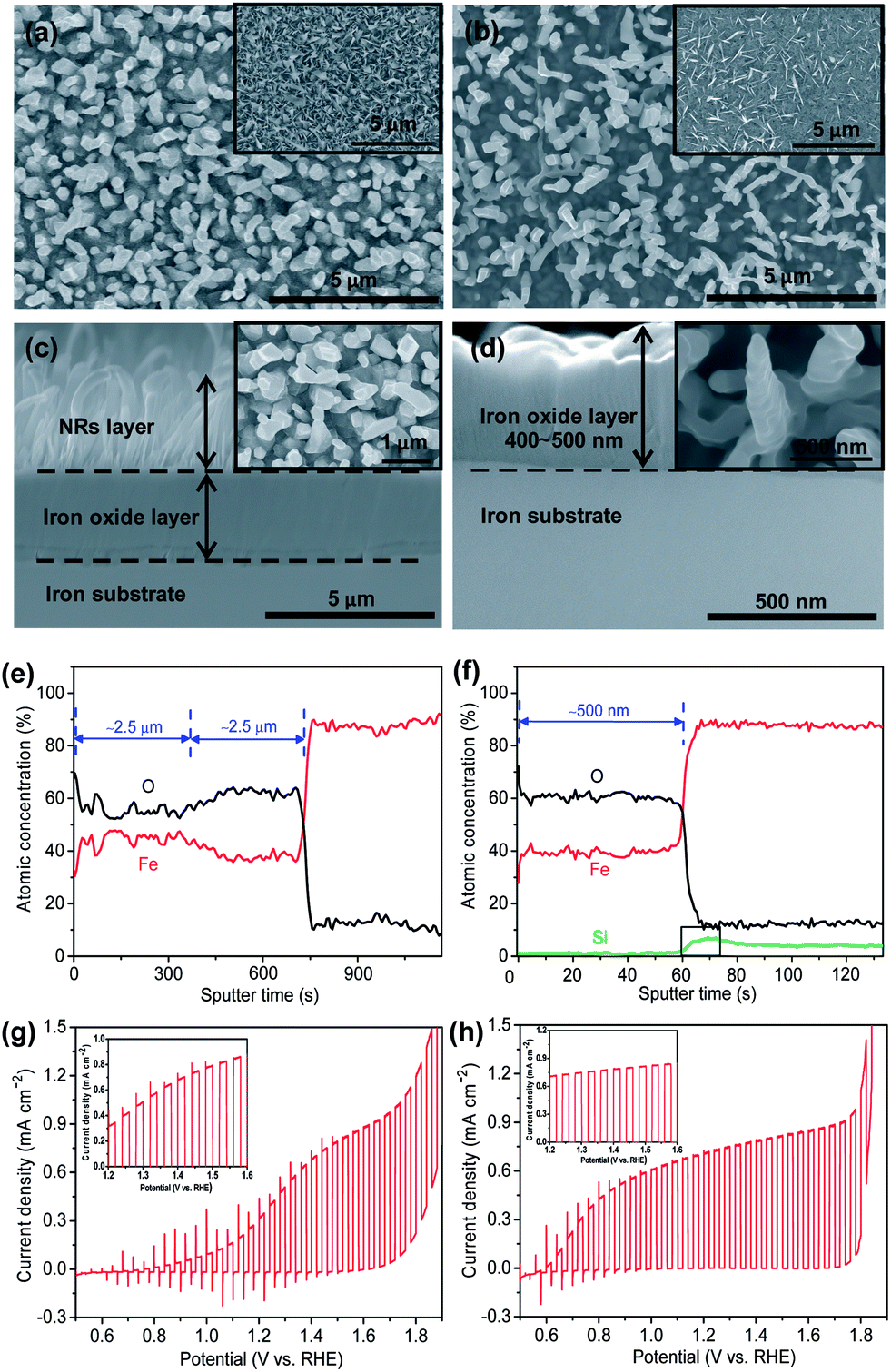 | ||
| Fig. 1 (a–d) SEM top views and cross-sections of oxide films resulting from (a and c) Fe and (b and d) Fe5Si alloy annealed at 500 °C for 0.5 h in air + 600 °C for 1 h in Ar. Insets of (a) and (b) show the top views of samples annealed at 500 °C for 0.5 h in air; insets of (c) and (d) show the high magnification of top views of (a) and (b); (e and f) corresponding element distribution of the oxide layer of the corresponding annealed (e) Fe and (f) Fe5Si alloy; (g and h) current–potential characteristics with chopped light of the annealed (g) Fe and (h) Fe5Si alloy. Inset graphs show magnified views of the 1.2–1.8 VRHE region for both spectra. Conditions: 1 M KOH solution (pH: 13.6), 2 mV s−1 scan rate. Photocurrents are excited with AM 1.5, 100 mW cm−2 simulated sunlight. | ||
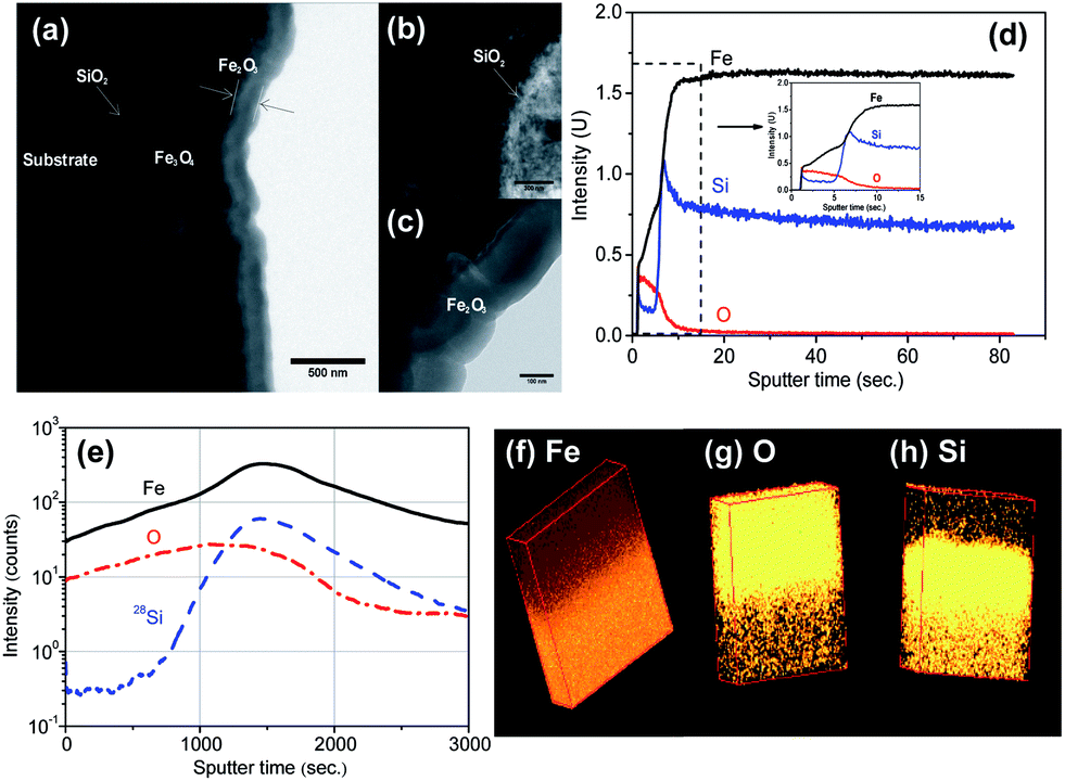 | ||
| Fig. 2 (a–c) TEM image of the annealed Fe5Si alloy; (d) GDOES elemental depth profiles of an oxide layer of the Fe5Si alloy; (e) ToF-SIMS depth profile for Fe, O, and Si species of the annealed Fe5Si alloy; (f–h) ToF-SIMS-EDS mapping of the Fe5Si alloy to show the distribution of Fe, O, and Si, respectively. | ||
Fig. 1g and h show the photoelectrochemical water splitting behavior under simulated sunlight AM 1.5 (100 mW cm−2) conditions in 1 M KOH for pure Fe and the Fe5Si alloy. From the transient-photocurrent vs. potential curves for pure Fe, upon sweeping the potential from 0.5 VRHE to 1.8 VRHE, the onset of water oxidation photocurrent is at 0.8 VRHE, and the photocurrent increases to 0.4 mA cm−2 at 1.23 VRHE. (A higher photocurrent is obtained for nanorod α-Fe2O3 than for the air annealed NF sample (ESI, Fig. S5a†).) For the Fe5Si alloy, most remarkably a significant cathodic shift of the onset potential up to 0.4 VRHE can be observed. This value is very close to the flat-band potential of α-Fe2O3 (0.4 VRHE) and among the most negative values ever reported.9
It is noteworthy that for the Fe–Si alloy the suboxide layer thickness is varied; X-ray diffraction (XRD) results (Fig. 3 and S6†) show stronger hematite peaks for the Fe–Si samples compared to the pure Fe, which indicates a higher crystallinity of the iron oxide structures for the Si containing substrates. This may be in line with reports on minor Si concentrations that affect the crystallinity of Fe2O3.1f The stronger (104) peak indicates that the c axis of the hexagonal hematite unit cell is aligned perpendicular to the substrate or the basal planes are aligned perpendicular to the substrate. Supported by both the TEM analysis and the dark current onset potentials, and in line with the literature,1f the SiO2 layer can act as an amorphous buffer that reduces the interfacial strain between the Fe substrate and Fe3O4–Fe2O3 layers. The reduced interfacial strain would directly lead to better Fe3O4–Fe2O3 film organization at an atomic level, and is seen to directly affect crystallinity (ESI, Fig. S7†). Moreover, the better crystallinity could reduce the boundary defects, which also may explain the improvement of the photocurrent onset potential.
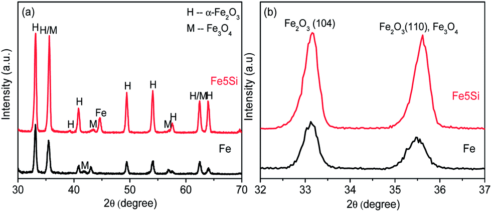 | ||
| Fig. 3 (a) XRD patterns of the oxide films resulting from Fe and Fe5Si alloy annealed at 500 °C for 0.5 h in air + 600 °C for 1 h in Ar and (b) high magnifications between 2θ = 32° and 37°. | ||
Fig. 4a shows the incident photocurrent conversion efficiencies (IPCEs) as a function of incident light wavelength for the Fe5Si alloy measured at various applied potentials. It is clear that the Fe5Si alloy leads to a significantly enhanced IPCE compared with pure Fe over the entire range from 300 nm to 550 nm. A beneficial effect of the Ar annealing can also be evaluated from the transient photoresponse (Fig. 4b). From the figures one can see that the transient ratio values (isteady/iinitial) close to one have been obtained compared to those in air annealing in the range of 0.02–0.86 (ESI, Fig. S8†). In general, the photo transient shape reflects strongly on the density and energy of the trapping states.2a,10,11 In light of XRD results, this can be attributed to the increased crystalline order within the nanorod structure after Ar annealing.
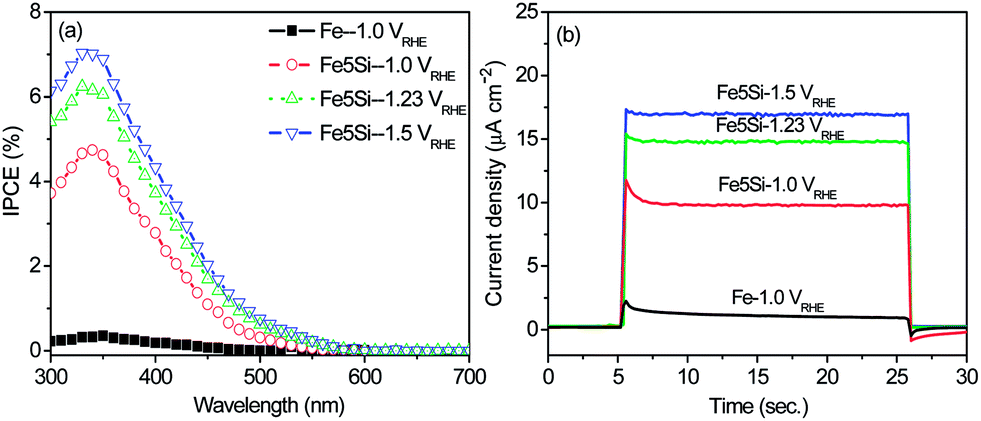 | ||
| Fig. 4 (a) The incident photon conversion efficiency (IPCE) and (b) photocurrent at 360 nm at applied potentials (1.0 VRHE, 1.23 VRHE, and 1.5 VRHE) in a 1 M KOH solution of the Fe5Si alloy annealed at 500 °C for 0.5 h in air + 600 °C for 1 h in Ar. | ||
In order to rule out the possibility that doping effects of the remaining Si in the Fe2O3 structure are the source of the shift in the onset potential, one may consider the following: according to earlier work,12 at least 1 at% Si needs to be present to clearly show a beneficial doping effect in hematite. However, if ToF-SIMS results (ESI, Fig. S9†) are quantified, only a Si concentration <0.2 at% in the oxide layer is at the maximum present. Therefore, the results presented here strongly suggest that the beneficial effect is due to the impact of crystallography of the iron oxide films and the strongly reduced Fe1−xO layer for the Fe5Si alloy.
Conclusions
In summary, in this work we grew oxide nanostructures by conventional thermal oxidation of Fe and FeSi alloys. A clearly improved water splitting performance is obtained for the Si containing alloy. Particularly, a remarkable cathodic shift of the onset potential up to 0.6 VRHE is observed for the Fe5Si alloy. This is one of the most negative onset potentials reported for hematite photoanode devices and is achieved without the use of other catalysts. We ascribe this strong beneficial effect to an accumulation of SiO2 at the metal–oxide interface – this Si-enriched layer hampers the formation of suboxides, namely Fe3O4, which is particularly detrimental to the performance of a hematite based water splitting anode and an increased crystallinity of the Fe2O3 layer among the layers formed on the Fe–Si alloy.Acknowledgements
We would like to acknowledge Dr Natalie Kömpel (Neue Materialien Fürch GmbH, NMF) for GDOES measurements. We thank DFG and the DFG cluster of excellence “Engineering of Advanced Materials” (EAM) for the financial support.Notes and references
- (a) A. Duret and M. Grätzel, J. Phys. Chem. B, 2005, 109, 17184 CrossRef CAS PubMed; (b) J. Brillet, M. Grätzel and K. Sivula, Nano Lett., 2010, 10, 4155 CrossRef CAS PubMed; (c) K. Sivula, F. L. Formal and M. Grätzel, ChemSusChem, 2011, 4, 432 CrossRef CAS PubMed; (d) K. Sivula, R. Zboril, F. L. Formal, R. Robert, A. Weiden kaff, J. Tucek, J. Frydrych and M. Grätzel, J. Am. Chem. Soc., 2010, 132, 7436 CrossRef CAS PubMed; (e) S. D. Tilley, M. Cornuz, K. Sivula and M. Grätzel, Angew. Chem., Int. Ed., 2010, 49, 6405 CrossRef CAS PubMed; (f) F. Le Formal, M. Grätzel and K. Sivula, Adv. Funct. Mater., 2010, 20, 1099 CrossRef CAS; (g) L. Wang, C.-Y. Lee and P. Schmuki, J. Mater. Chem. A, 2013, 1, 212 RSC; (h) L. Wang, A. Palacios-Padrós, R. Kirchgeorg, A. Tighineanu and P. Schmuki, ChemSusChem, 2014, 7, 421 CrossRef CAS PubMed.
- (a) M. Frites and S. U. M. Khan, ECS Trans., 2009, 19, 137 CAS; (b) H. G. Kim, P. H. Borse, J. S. Jang, C. W. Ahn, E. D. Jeong and J. S. Lee, Adv. Mater., 2011, 23, 2088 CrossRef CAS PubMed; (c) C.-Y. Lee, L. Wang, Y. Kado, S. Killian and P. Schmuki, ChemSusChem, 2014, 7, 934 CrossRef CAS.
- (a) M. P. Dareedwards, J. B. Goodenough, A. Hamnett and P. R. Trevellick, J. Chem. Soc., Faraday Trans., 1983, 79, 2027 RSC; (b) J. B. Goodenough, Prog. Solid State Chem., 1971, 5, 145 CrossRef CAS; (c) J. H. Kennedy and J. K. W. Frese, J. Electrochem. Soc., 1978, 125, 709 CrossRef CAS PubMed.
- (a) P. Hiralal, S. Saremi-Yarahmadi, B. C. Bayer, H. Wang, S. Hofmann, K. G. Upul Wijayantha and G. A. Amaratunga, Sol. Energy Mater. Sol. Cells, 2011, 95, 1819 CrossRef CAS PubMed; (b) T. Vincent, M. Gross, H. Dotan and A. Rothschild, Int. J. Hydrogen Energy, 2012, 37, 8102 CrossRef CAS PubMed; (c) L. Wang, C.-Y. Lee, A. Mazare, K. Lee, J. Müller, E. Spiecker and P. Schmuki, Chem. – Eur. J., 2014, 20, 77 CrossRef CAS PubMed.
- (a) X. Wen, S. Wang, Y. Ding, Z. L. Wang and S. Yang, J. Phys. Chem. B, 2005, 109, 215 CrossRef CAS PubMed; (b) A. G. Nasibulin, S. Rackauskas, H. Jiang, Y. Tian, P. R. Mudimela, S. D. Shandakov, L. I. Nasibulina, J. Sainio and E. I. Kauppinen, Nano Res., 2009, 2, 373 CrossRef CAS PubMed.
- (a) Q. Yang, H. Kukino and H. J. Tatsuoka, Nanosci. Nanotechnol., 2010, 10, 7795 CrossRef CAS PubMed; (b) X. Su, C. Yu and C. Qiang, Appl. Surf. Sci., 2011, 257, 9014 CrossRef CAS PubMed; (c) B. D. Chernomordik, H. B. Russell, U. Cvelbar, J. B. Jasinski, V. Kumar, T. Deutsch and M. K. Sunkara, Nanotechnology, 2012, 23, 194009 CrossRef PubMed.
- (a) N. Beermann, L. Vayssieres, S. E. Lindquist and A. Hagfeldt, J. Electrochem. Soc., 2000, 147, 2456 CrossRef CAS PubMed; (b) Z. Chen, U. Cvelbar, M. Mozetic, J. He and M. K. Sunkara, Chem. Mater., 2008, 20, 3224 CrossRef CAS; (c) U. Bjorksten, J. Moser and M. Grätzel, Chem. Mater., 1994, 6, 858 CrossRef.
- (a) I. Svedung and N. G. Vannerberg, Corros. Sci., 1974, 14, 391 CrossRef CAS; (b) T. Adachi and G. H. Meier, Oxid. Met., 1987, 27, 347 CrossRef CAS; (c) J. Kucera and M. Hajduga, High temperature and long time oxidation of iron and steels, Wydawnictwo PL Filia W, Bielsku-Bialej, 1998, vol. 15 Search PubMed; (d) T. Ban, K. Bohnenkamp and H. J. Engell, Corros. Sci., 1979, 19, 291 CrossRef; (e) A. R. Lashin, O. Schneeweiss and Y. Houbaert, Corros. Sci., 2008, 50, 2580 CrossRef CAS PubMed.
- M. T. Mayer, C. Du and D. Wang, J. Am. Chem. Soc., 2012, 134, 12406 CrossRef CAS PubMed.
- (a) N. Birks, G. H. Meier and F. S. Pettit, Introduction to the high temperature oxidation of metals, Cambridge University Press, Cambridge, New York, 2nd edn, 2006 Search PubMed; (b) M. A. Lukowski and S. Jin, J. Phys. Chem. C, 2011, 115, 12388 CrossRef CAS.
- P. Iwanski, J. Curran, W. Gissler and R. Memming, J. Electrochem. Soc., 1981, 128, 2128 CrossRef CAS PubMed.
- (a) J. H. Kennedy, M. Anderman and R. Shinar, J. Electrochem. Soc., 1981, 128, 2371 CrossRef CAS PubMed; (b) J. H. Kennedy, R. Shinar and J. P. Ziegler, J. Electrochem. Soc., 1981, 127, 2307 CrossRef PubMed; (c) C.-Y. Lee, L. Wang, Y. Kado, R. Kirchgeorg and P. Schmuki, Electrochem. Commun., 2013, 34, 308 CrossRef CAS PubMed.
Footnote |
| † Electronic supplementary information (ESI) available. See DOI: 10.1039/c3mh00173c |
| This journal is © The Royal Society of Chemistry 2014 |