 Open Access Article
 This Open Access Article is licensed under a
 Creative Commons Attribution 3.0 Unported Licence
Grazing incidence X-ray fluorescence of periodic structures – a comparison between X-ray standing waves and geometrical optics calculations
Falk
Reinhardt†
a,
Stanisław H.
Nowak‡
*b,
Burkhard
Beckhoff
a,
Jean-Claude
Dousse
b and
Max
Schoengen
c
aPhysikalisch-Technische Bundesanstalt (PTB), Abbestr. 2-12, D-10587 Berlin, Germany
bPhysics Department, University of Fribourg, Ch. du Musée 3, CH-1700 Fribourg, Switzerland. E-mail: nowak@ifg-adlershof.de
cInstitute for Nanometre Optics and Technology, Helmholtz-Zentrum Berlin (HZB), Albert-Einstein-Str. 15, D-12489 Berlin, Germany
First published on 3rd July 2014
Abstract
Grazing incidence X-ray fluorescence spectra of nano-scaled periodic line structures were recorded at the four crystal monochromator beamline in the laboratory of the Physikalisch-Technische Bundesanstalt at the synchrotron radiation facility BESSY II. For different tilt angles between the lines and the plane of incidence of the monochromatic synchrotron radiation, spectral features are observed which can be understood and explained with calculations of the emerging X-ray standing wave (XSW) field. On the other hand, there are structures, i.e., pronounced modulations above the substrate's critical angle of external total reflection, which are not included in the XSW concept. Novel geometrical optics calculations can reproduce these structures taking the sample's specific geometric conditions into account.
1 Introduction
Analytical methods which allow for reliable characterization of nanostructured surfaces are in demand in a variety of fields that range from environmental analysis to industrial process control. Beside merely the size information, the inner structure of nanoparticles or nanostructures accompanied with elemental or even chemical analysis is needed. Also a quantitative assessment of the number or mass of particles often has to be provided.Grazing incidence X-ray fluorescence analysis (GIXRF)1 has proven to be one of the suitable methods for the characterization of near-surface structures like layers, ion implantations2 and nanoparticles deposited on flat surfaces.3 In this method the very low detection limit of total reflection XRF (TXRF)4,5 is combined with the possibility of determining the depth of the structure in the nanometer scale. Complementary characterisation methods such as GISAXS6 and MEIS7 have been also applied to nanostructures and nanoparticles, aiming mainly at dimensional information such as the shape and size while X-ray spectrometric methods directly provide compositional information needed for elemental analysis or chemical speziation.
The size resolution of GIXRF is enabled by angle-dependent behavior of the effective excitation intensity above the substrate and into the depth which is conveniently explained by the occurrence of an X-ray standing wave field (XSW). This XSW forms due to a coherent superposition of the incident and the reflected beam8 and it can be calculated with existing software codes, such as IMD.9
With a good knowledge of the spatial distribution of the XSW and the effective excitation intensity of the sample, even reference-free X-ray fluorescence analysis is enabled.10,11 This is of special interest for the analysis of nano-scaled systems since the number of samples to be quantitatively analyzed grows much faster than the number of appropriate, i.e., sufficiently similar, reference materials.
In the case of particle-like surface contaminations, especially for nanoparticles, XSW calculations yield reliable intensity distributions only as long as the particles deposited on the surface can be considered as isolated particles and interact with an undisturbed XSW.8 With increasing deposition density the particles start to interact with an XSW that is modified by other particles. For that reason XSW calculations need to incorporate some means to describe particular surface conditions such as surface roughness or geometry modifying factors.12 However, they are still subject to wrong intensity distributions and higher uncertainties of the results.13
Recently a complementary Geometrical Optics (GO)-based approach was developed to overcome the shortcomings of XSW calculations.14 In this ray tracing model the path of each X-ray within the sample is computed, taking into consideration any intermediate reflection, refraction or transmission at horizontal and vertical interfaces. The phase shifts corresponding to all possible pathways are calculated and the probability of each photon to interfere with itself is determined. Since the ray tracing calculations are insensitive to the direction of the path, the GO method can be applied indifferently to GIXRF and GEXRF (Grazing Emission XRF) measurements.15 For the intensity calculation of the fluorescence radiation emitted by periodic surface structures, the GO approach is certainly more efficient than the one-dimensional XSW method. In particular, the periodicity of the structure is easily parameterizable and thus, specific geometrical boundary conditions can be taken into consideration.16
To investigate the differences between the two theoretical approaches and to check the reliability of XSW calculations for quantitative GIXRF measurements on highly structured surfaces, a periodic arrangement of chromium stripes on a silicon substrate was produced (see Fig. 1). This sample allows for a continuous change between layer-like and particle-like behavior by simply turning the direction of the surface structures against the plane of incidence of the excitation radiation, i.e., a change of φ in Fig. 2. The Cr stripes were nanoscaled in height and can be considered an idealized model for monodisperse nanoparticles with a very shallow size distribution when, with increasing deposition density, they transition to nanolayers.
 | ||
| Fig. 1 SEM picture of a 15 × 25 μm2 detail of the sample surface. The stripes have a width of 1 μm and a spacing of 5 μm. The height of 10 nm and the flatness of the Cr stripes were validated with additional AFM measurements. | ||
 | ||
| Fig. 2 Principle layout of the sample. The Cr stripes are parallel to the y-axis and lie in the x-y-plane. The angle between the incident radiation and the x-y-plane is represented by ϑ; the tilt angle between the y-axis and the projection of the incident beam on the x-y-plane is denoted by φ. | ||
The XRF measurements were performed at the four-crystal monochromator beamline17 in the laboratory of the Physikalisch-Technische Bundesanstalt (PTB) at the synchrotron radiation facility BESSY II18 with a novel instrumentation developed for reference-free XRF nanoanalytics.19 In the present measurements the tilt angle φ (see Fig. 2) was varied between 0° and 90°, whereas the incidence angle ϑ was varied from 0° to the fourfold value of the critical angle for external total reflection at the silicon substrate, i.e., to about 1.2° for the preset incoming photon energy of 7 keV. The fluorescence intensity measured at each incident angle was then compared to calculated XSW excitation intensities and to the intensities obtained from GO calculations.
2 Samples and experiment
The sample was prepared using a lift-off technique.20 At first, an inverse pattern of 1000 parallel grooves having a length of 6 mm, a width of 1 μm and a spacing of 5 μm was imprinted on a 1 × 1 cm2 PMMA-coated silicon substrate by means of electron beam lithography, using an electron beam with a diameter of 20 nm. The patterned photoresist film was then covered with the target material, i.e., a 10 nm thick chromium layer. After washing out the sacrificial material (photoresist) together with the target material on its surface, a pattern of 10 nm high and 1 μm wide Cr stripes having a periodicity of 6 μm and an effective area of 6 × 6 mm2 remained on the substrate surface (see Fig. 1). Note that the removal of the sacrificial material being not so easy for such a pattern, the sample was immersed in the solvent for a longer time than usual, i.e., about 12 h.The sample was mounted on a multi-axis manipulator in a recently developed ultra-high vacuum chamber of the PTB.19 This chamber features an x-y-z-sample stage on a ϑ-χ-φ-manipulator. Here χ denotes the angle between the sample surface and the polarization plane of the incident synchrotron beam. Thus, for χ = 0°, measurements of s-polarized photons are possible whereas χ = 90° allows minimizing the detected scattering radiation produced in a sample. For a value of χ = 90°, ϑ is the angle of the incident beam with respect to the substrate surface. This angle can be varied from 0° to 45°, enabling both GIXRF and TXRF measurements as well as conventional XRF measurements in the standard 45°/45°-geometry. The φ-stage rotates the mounted sample around the normal vector of the sample surface.
As shown in Fig. 2, for the considered sample, the stripes are defined to run in the x-y-plane along the y-axis. Therewith the rotation around the z-axis is expressed via the value of φ and φ = 0 denotes the position, where the stripes are parallel to the plane of incidence. The grazing angle with respect to the sample surface is denoted by ϑ.
For the measurements, the sample was aligned so that the center of the stripe structure coincided with the ϑ and φ rotation centers. Then the angle φ was varied in steps of 1° for tilt angles from −3° to 3°. For 5° ≤ φ ≤ 85° the angular step width was set to 5° and around φ = 90° decreased to 1° again. At each angle φ, the Cr-Kα count rate was recorded with a SDD detector, varying the incident angle ϑ from 0° to 1.2° with a step width of 0.01°. For incident radiation with an energy of 7 keV the critical angle for external total reflection at the silicon substrate is ϑc,Si = 0.26° and for the chromium layer ϑc,Cr = 0.39°.21
The obtained angular profiles were normalized to account for the number of incident photons which was monitored using a thin transmission diode and to the angle dependent effective solid angle of detection. Applying the known detector efficiency22 the detected count rate for the Cr-Kα line can be converted to the emitted Cr-Kα fluorescence intensity.
For the considered sample, the maximum chromium layer thickness that any emitted photon must pass in order to reach the detector is around 10 nm. Thus, self-absorption effects can be neglected and the fluorescence intensity can be assumed to be proportional to the effective excitation intensity at the point where the incident X-rays have been absorbed. Thus, the measured fluorescence intensities can be directly compared to theoretical intensities calculated using the XSW and GO approach, respectively.
3 Calculations
3.1 X-ray standing wave field calculations
If the sample is excited along the stripes (φ = 0), two distinct interactions between the sample and the incident beam can take place: either the beam impinges onto the Cr stripes, then the interaction is that of a closed Cr layer, or the beam hits the Si substrate, then above the Si substrate the usual undisturbed XSW emerges along the beam propagation direction. In the latter case, since the sidewalls of the stripes are parallel to the propagation direction, there is no significant interaction with chromium. Thus, in the angle dependent Cr signal only the contribution of a 10 nm layer is to be expected.For all tilt angles φ ≠ 0 the interaction of the Cr sidewall signal with the XSW which forms above the Si surface should be considered. This interaction leads to an angular profile which is similar to the one that would be observed with a thin non-absorbing Cr layer5 or with a particle-like Cr structure deposited on a Si substrate.
According to above considerations, one should be able to simulate the excitation intensity of the chromium structures by a simple linear combination of the two corresponding XSW contributions.
The X-ray standing wave field intensities were calculated for the incident photon energy of 7 keV using the IMD software package.9 Two independent components were considered: the contribution of the layer-like structure consisting of a 10 nm thick chromium layer on a Si bulk and the undisturbed particle-like signal, which is obtained from the calculation of the XSW above a flat Si substrate and successive integration over the first 10 nm. In Fig. 3 the recorded GIXRF spectra for tilt angles φ from 0° to 8° are shown and compared to the two distinct XSW contributions. From the figure one can see that this simple approach leads to very satisfying results for low tilt angles φ.
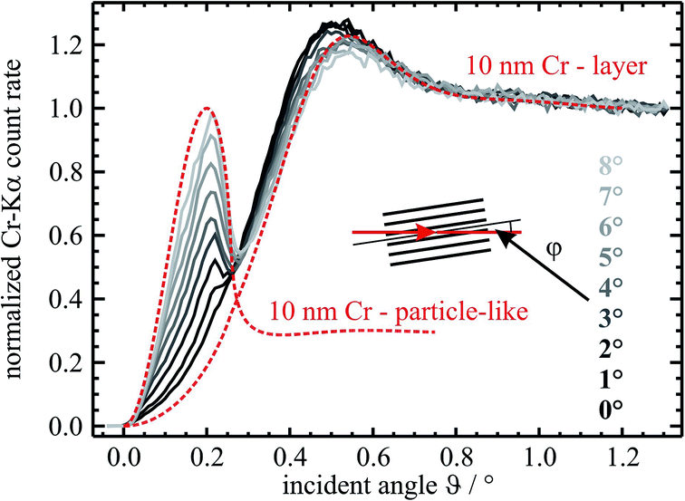 | ||
| Fig. 3 Grazing incidence XRF data for tilt angles φ from 0° to 8°. For φ = 0° the measured spectrum follows the shape of the XSW field produced by a 10 nm chromium layer. For all other tilt angles the angular profile shows an additional feature which corresponds to particle-like chromium contamination on a Si wafer. As shown, this feature becomes more intense for larger φ. | ||
3.2 Geometrical optics calculations
For the GO calculations a dedicated software program was developed.14 The software is based on a reverse ray tracing approach tracking the full evolution of a plane wave from the point where the photon is absorbed to the point where it penetrates into the structure. Note that, according to the Stokes–Helmholtz reversion-reciprocity principle, this reverse ray tracing is completely equivalent to the more intuitive direct ray tracing which follows the photon propagation. The program traces all possible ray paths of the photon taking into consideration the radiation amplitude evolution due to absorption, reflection, refraction, and transmission at horizontal and vertical interfaces. From the differences in the phase shifts associated with the simulated ray paths, the program calculates the probability for each photon to interfere with itself.Due to the simple geometrical properties of the investigated chromium stripe sample (constant height of the stripes and only horizontal and vertical interfaces) the number of ray paths required for the calculations remains well tractable for the program. Indeed, for a given incident radiation direction, the refraction into the chromium structure can be realized in two manners only – at a horizontal or a vertical interface. Furthermore, a ray passing through the vacuum between two chromium stripes does not change its direction, and the radiation reflected at the vertical interfaces can be neglected as in the X-ray regime the reflectivity quickly reaches zero for large angles of incidence.
Thus, at a given fluorescence point only four final ray path directions have to be considered: two ray path directions (up and down) for the incident radiation reaching the structure from horizontal interfaces and two ray path directions (up and down) for the incident radiation reaching the structure from vertical interfaces. Additional ray paths should be taken into account when there are multiple reflections at horizontal interfaces. In this case, a given fluorescence point is reached after 0, 1, 2, etc. reflections (see Fig. 4).
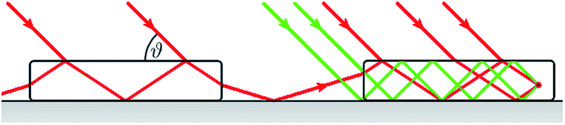 | ||
| Fig. 4 Schematic view of various ray paths reaching the same fluorescent point. Ray paths penetrating the structure from horizontal interfaces are represented with red lines and those from vertical interfaces by green lines. For a given incident angle only four final ray path directions are possible. | ||
In order to obtain information about the whole sample, the ray tracing calculations were performed for many fluorescent points. The latter were assumed to be distributed uniformly within the Cr stripes. However, owing to the periodicity of the structure, only the fluorescent points of a single stripe had to be considered. For excitation along the stripes (φ = 0) the ray tracing procedure was performed only for reflections at horizontal interfaces. Thus the obtained results are equivalent to those of a closed Cr layer. For all tilt angles φ ≠ 0 the computations were performed using a larger width 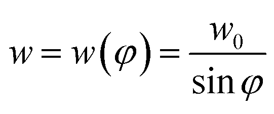 and a larger periodicity
  of the stripes.
4 Results
In Fig. 5 the experimental angular profiles of the periodic chromium sample (top panel) are compared to those obtained from the XSW and GO simulations. As expected, for excitation along the stripes (φ = 0) measurements exhibit a pure layer-like profile. For larger tilt φ the layer-like component disappears gradually and a particle-like signal resulting from the Cr stripe sidewalls arises in the spectra.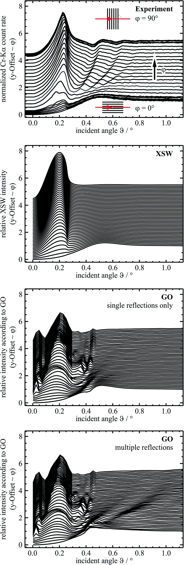 | ||
| Fig. 5 Comparison between the measured angle-dependent Cr-Kα fluorescence intensity (top panel) and the excitation intensities calculated according to the X-ray standing wave approach (2nd panel from the top) and the geometrical optics one for single reflections only (3rd panel from the top) and multiple reflections (bottom panel). | ||
In this respect the simple XSW superposition of the two contributions (see 2nd panel) shows quite good agreement with the experimental results. There is, however, a striking difference in the shape of the particle-like feature. The measured peaks are significantly sharper than the calculated ones. It is safe to assume that shadowing is the origin of this discrepancy. For very shallow angles the incident radiation cannot reach the substrate in between two subsequent structures without having to pass through the first structure.23 The resulting attenuation, scattering, phase shift and change of direction of the incident radiation prevent the formation of an undisturbed XSW above the silicon surface.
For φ > 20° (light gray curve in the top panel) the measured spectra are dominated by the particle-like signal and additional intensity modulations can be observed. The latter are clearly visible above the critical angle of external total reflection at the substrate. The angular separation between two consecutive intensity modulation maxima evolves with the tilt angle φ. Thus, the observed variation is due to the change of either the structure periodicity p(φ) or stripe width w(φ). These modulations cannot be seen in the XSW simulation.
The 3rd panel of Fig. 5 shows the GO results when each incident photon is reflected only once at the substrate. The layer-like and the particle-like features are well reproduced. For incident angles between roughly 0.3° and 0.5° additional small peaks and dents can be seen for different tilt angles which are not visible in the XSW results or in the experimental data. This angular range is above the critical angle of the substrate. Therefore X-rays are not reflected at the vacuum/Si interface. At the Cr/Si interfaces within the structures, however, total reflection can take place. Therefore, the sharp peaks observed in the GO simulations originate most likely from numerical residues of this effect.
The results of GO simulations including the multiple reflections of X-rays at the Si substrate and/or at the Cr structures themselves are depicted in the bottom panel of Fig. 5. As shown, the consideration of the multiple reflections in the GO calculations permits reproducing quite well the additional intensity modulations observed in the experimental profile.
Thus, according to these GO simulations the angular positions of the intensity modulation maxima can be understood as the incident angles for which the number of possible ray paths reaching the fluorescence emission point is significantly higher than for other angles. This situation occurs whenever the distance between consecutive reflections on the top or bottom interfaces of the structure is a fraction or a multiple of the structure's period (see Fig. 6).
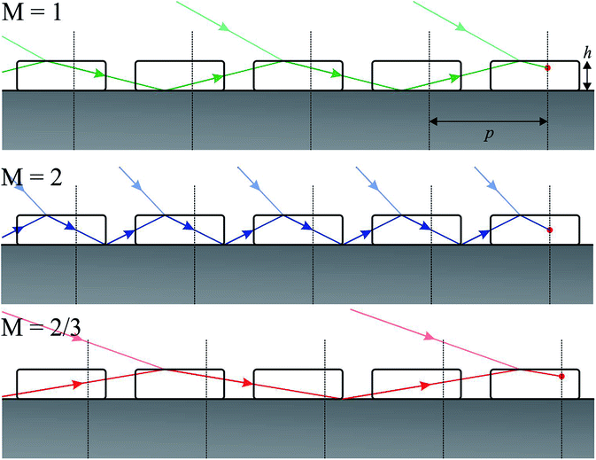 | ||
| Fig. 6 Sketch showing possible ray paths for multiple reflections. M stands for the number of reflections which take place within one period of the structure (see eqn (1)). | ||
Neglecting the refraction of the X-rays at the side interfaces of the structure, the angles at which these modulation maxima are observed can be determined from the following relation:
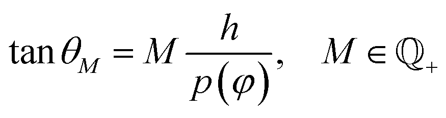 | (1) |
If the radiation reaches the structure from the top interface, the angle of incidence ϑ is given by:
cos![[thin space (1/6-em)]](https://www.rsc.org/images/entities/char_2009.gif) ϑ = nCrcosθ ϑ = nCrcosθ | (2) |
Substituting p(φ) with p0/sinφ we can write the condition for modulation maxima as follows:
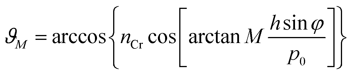 | (3) |
Thus, the angular positions of the modulation intensity maxima can be calculated directly from the refractive index nCr, height h and period p0 of the Cr structure, and the tilt angle φ.
This simple formula, however, omits the imaginary part of the refractive indices of the materials. Therefore it is valid only for angles well above the critical angle of total reflection. As shown in Fig. 7, for ϑ ≳ 0.5° the angular positions of the modulation maxima (dotted lines) are indeed well reproduced for each value of M. In contrast, close to the critical angle the approximation becomes increasingly inaccurate. For this reason, additional GO calculations were performed in which the refractive indices were included. The refractive indices are represented by complex numbers n = 1 − δ − βi, where both δ and β are constant numbers which are small in the energy regime of X-rays. For the incident energy of 7 keV the tabulated optical constants of Cr are δ = 2.6956 × 10⁻⁵ and β = 3.5512 × 10−6.21
 | ||
| Fig. 7 Contour plot of the measured Cr-Kα fluorescence intensity. The curves stand for the calculated angular positions ϑM of the modulation intensity maxima for M = 3, 6 and 8. The results obtained from eqn (3) are represented by the dotted lines. As shown, with this equation, which does not take into consideration the imaginary part of the refractive index, the angular positions of the maxima tend to the Cr critical angle for total reflection when the tilt angle φ tends to zero. The dashed lines show the results obtained from GO calculations using tabulated values for the optical constants, whereas the solid lines correspond to GO calculations in which the imaginary part of the refractive index was adjusted (see text). | ||
Using these values in the GO calculations, better but still not completely satisfactory agreement was observed with the experimental data (see the dashed lines in Fig. 7). We found that good agreement can be, however, achieved if the imaginary part of the Cr refractive index is increased by a factor of about 2. With this adjusted value for the optical constant β, the angular positions of the modulation maxima are well reproduced by the GO calculations, also in the angular region close and below the critical angle (see the solid lines in Fig. 7). As the intensity attenuation of the radiation in matter is accounted for by the imaginary part of the refractive index, we are inclined to believe that the needed increase of the optical constant β reflects the additional loss of intensity due to the roughness of the reflecting and refracting interfaces.
5 Conclusions
X-ray standing wave field calculations and the geometrical optics approach are complementary methods to describe the intensity modulations observed in the GIXRF angular profiles of flat surfaces excited by X-ray beams under very shallow incidence angles. The XSW approach allows fast calculations and, within the accuracy of the optical constants, provides reliable results for homogeneous surfaces and layers. However, for periodic surface structures some features of the measured angular profiles cannot be reproduced by the present XSW approach. For such types of structured surfaces the geometrical optic-based ray tracing method is more suitable although the GO calculations can be significantly more time-consuming.In the GIXRF angular profiles of the Cr sample investigated in this work, namely a periodic pattern of parallel Cr stripes, layer-like and particle-like features are prominent. The two features were found to be reliably described by XSW and GO simulations. Additional intensity modulations which are related to the periodicity of the structured surface were found in the recorded GIXRF profiles. These modulations could be reproduced by the GO simulations, provided multiple reflections of X-rays are taken into account in the calculations and adequate values are adopted for the refraction indices. In particular, it was shown that the use of tabulated values for the real and imaginary parts of the Cr refraction index leads to some disagreement between the GO predictions and the experimental data in the angular regions close to the critical angle and below it. However, it was found that this discrepancy can be removed by choosing for the imaginary part of the Cr refraction index a value about two times larger than the tabulated one. This intriguing observation was tentatively explained by the roughness of the interfaces which can contribute to the increase of attenuation of the X-rays within the sample.
6 Outlook
The GIXRF technique combined with XSW and GO modeling represents a powerful tool for the assessment of nano-scaled surface structures. More complex patterns comprising micro- and nanostructures also with varying inner compositions have already been tested using the presented approach.14,16It was shown that GIXRF profiles of some nanolayered particulate systems, such as 2 nm thick Au coatings on 100 nm high Cr structures, can be well explained with XSW simulations.12 With the use of XSW modeling it was also shown that GIXRF is sensitive to differently shaped particles, i.e., spheres, cylinders or cuboids.8,24 Under ideal conditions, i.e., monodisperse high-Z element nanoparticles on clean flat substrates, size differences even in the sub-nanometer range can be resolved by comparing measured GIXRF profiles to XSW calculations. For surfaces with roughness above 1 nm, high energy X-ray standing waves will start to degrade, blurring the characteristic angular profiles. Also particle size distributions with FWHM of more than 20% of the mean particle diameter complicate the size discrimination. Superpositions of well-defined particle sizes on the other hand can be deconvolved using appropriate software tools.
In situation, however, where, due to scattering and absorption effects, it is no longer safe to assume an undisturbed XSW, the GO approach can be applied advantageously. A restriction for the use of the GO approach for unknown sample systems is that it needs information on the structure morphology as an input parameter. Usually this information is obtained from preceding SEM or AFM measurements. A tempting perspective is to use the grazing incidence conditions for simultaneous detection of GIXRF and GISAXS signals. The GISAXS technique is a well-established methodology to retrieve the dimensional information on the surface structure which in turn can be used as input for the calculation of the effective excitation intensity. In this way, size and structural information can be obtained with high element sensitivity and with reference-free quantitative analysis of each elements mass deposition.
References
- A. von Bohlen, Spectrochim. Acta, Part B, 2009, 64, 821–832 CrossRef PubMed.
- P. Hönicke, B. Beckhoff, M. Kolbe, D. Giubertoni, J. van den Berg and G. Pepponi, Anal. Bioanal. Chem., 2010, 396, 2825–2832 CrossRef PubMed.
- M. Tiwari, G. Bhalerao, M. Babu, A. Sinha and C. Mukherjee, J. Appl. Phys., 2008, 103, 054311 CrossRef PubMed.
- P. Wobrauschek and H. Aiginger, Anal. Chem., 1975, 47, 852–855 CrossRef CAS.
- R. Klockenkämper, Total-reflection X-Ray Fluorescence Analysis, John Wiley & Sons, Inc., 1997 Search PubMed.
- G. Renaud, R. Lazzari and F. Leroy, Surf. Sci. Rep., 2009, 64, 255–380 CrossRef CAS PubMed.
- M. Sortica, P. Grande, G. Machando and L. Miotti, J. Appl. Phys., 2009, 106, 114320 CrossRef PubMed.
- A. von Bohlen, M. Krämer, C. Sternemann and M. Paulus, J. Anal. At. Spectrom., 2009, 24, 792–800 RSC.
- D. Windt, Comput. Phys., 1998, 4, 360–370 CrossRef PubMed.
- B. Beckhoff, R. Fliegauf, M. Kolbe, M. Müller, J. Weser and G. Ulm, Anal. Chem., 2007, 79, 7873–7882 CrossRef CAS PubMed.
- B. Beckhoff, J. Anal. At. Spectrom., 2008, 23, 845–853 RSC.
- F. Reinhardt, J. Osán, S. Török, A. Pap, M. Kolbe and B. Beckhoff, J. Anal. At. Spectrom., 2012, 27(2), 248–255 RSC.
- K. Tsuji, T. Yamada, T. Utaka and K. Hirokawa, J. Appl. Phys., 1995, 78, 969–973 CrossRef CAS PubMed.
- S. F. Reinhardt, B. Beckhoff, J.-Cl. Dousse and J. Szlachetko, J. Anal. At. Spectrom., 2013, 28, 689–696 RSC.
- P. Hönicke, Y. Kayser, B. Beckhoff, M. Müller, J.-Cl. Dousse, J. Hoszowska and S. H. Nowak, J. Anal. At. Spectrom., 2009, 27, 1432–1438 RSC.
- S. H. Nowak, D. Banaś, W. Błachucki, W. Cao, J.-Cl. Dousse, P. Hönicke, J. Hoszowska, L. Jabłoński, Y. Kayser, A. Kubala-Kukuś, M. Pajek, F. Reinhardt, A. V. Savu and J. Szlachetko, Spectrochim. Acta, Part B, 2014, 98, 65–75 CrossRef CAS PubMed.
- M. Krumrey, J. Synchrotron Radiat., 1998, 5, 6–9 CrossRef CAS PubMed.
- B. Beckhoff, A. Gottwald, R. Klein, M. Krumrey, M. Müller, M. Richter, F. Scholze, R. Thornagel and G. Ulm, Phys. Status Solidi B, 2009, 246, 1415–1434 CrossRef CAS.
- J. Lubeck, B. Beckhoff, R. Fliegauf, I. Holfelder, P. Hönicke, M. Müller, B. Pollakowski, F. Reinhardt and J. Weser, Rev. Sci. Instrum., 2013, 84, 045106 CrossRef CAS PubMed.
- Z. Cui, Nanofabrication: Principles, Capabilities and Limits, Springer, 2008 Search PubMed.
- B. Henke, E. Gullikson and J. Davis, At. Data Nucl. Data Tables, 1993, 54, 181–342 CrossRef CAS.
- F. Scholze and M. Procop, X-Ray Spectrom., 2001, 30, 69–76 CrossRef CAS.
- U. Fittschen, M. Menzel, O. Scharf, M. Radke, U. Reinholz, G. Buzanich, V. Montoya, K. McIntosh, C. Streli and G. Havrilla, Spectrochim. Acta, Part B, 2014, 99, 179–184 CrossRef PubMed.
- A. von Bohlen, M. Brücher, B. Holland, R. Wagner and R. Hergenröder, Spectrochim. Acta, Part B, 2010, 65, 409–414 CrossRef PubMed.
Footnotes |
| † Present address: Bruker Nano GmbH, Am Studio 2D, D-12489 Berlin, Germany. |
| ‡ Present address: IfG - Institute for Scientific Instruments GmbH, Rudower Chaussee 29/31, D-12489 Berlin, Germany. |
| This journal is © The Royal Society of Chemistry 2014 |