 Open Access Article
 This Open Access Article is licensed under a Creative Commons Attribution-Non Commercial 3.0 Unported Licence
Gel electrophoresis using a selective radical for the separation of single-walled carbon nanotubes
Sara
Mesgari
,
Ashok Kumar
Sundramoorthy
,
Leslie S.
Loo
* and
Mary B.
Chan-Park
*
School of Chemical & Biomedical Engineering, Nanyang Technological University, 62 Nanyang Drive, Singapore 637459, Singapore. E-mail: mbechan@ntu.edu.sg; Fax: +65 6794 7553; Tel: +65 6790 6064
First published on 9th June 2014
Abstract
We have applied agarose gel electrophoresis (AGE) to single-walled carbon nanotubes (SWNTs) that have been pre-reacted with metallic-selective ionic radicals and then re-suspended with sodium cholate (SC) surfactant to obtain highly purified (up to 98%) semiconducting single-walled carbon nanotubes (s-SWNTs). The proposed combination method exploits the preferential reactivity with the metallic nanotube of the radicals generated from an azo naphthalene compound (Direct Blue 71 (I)) to preferentially increase the surface charge, and therefore the electrophoretic mobilities, of the metallic nanotube population under the influence of the electric field in AGE. The excellent separation achieved was verified by UV-vis-NIR and Raman spectroscopy as well as by the performance of field effect transistors fabricated with semiconducting-enriched SWNTs. FETs fabricated with I-assisted AGE-separated semiconducting nanotubes exhibited mobilities of ∼3.6 to 11.7 cm2 V−1 s−1 and on/off ratios from 102 to 106.
1. Introduction
Current state-of-the-art single-walled carbon nanotube (SWNT) synthesis methods invariably produce mixtures of metallic (m-SWNTs) and semiconducting (s-SWNTs) nanotubes. However, most electronic applications of SWNTs, such as in nanoelectronics and thin film transistors, require electronically homogeneous SWNTs, i.e. either metallic or semiconducting species. The electronic heterogeneity of SWNTs is a major obstacle to the widespread use of SWNTs in electronic applications. If not electronically purified, the parasitic effects of the unwanted type of SWNT significantly degrade the properties of the devices made with these nanotubes. Various metallicity-based separation techniques have been proposed to separate metallic from semiconducting nanotubes, including covalent or non-covalent selective chemistry, chromatography, and density-gradient ultracentrifugation.1–4 However, ultra-high purity (>98%) and high process yield/throughput techniques which can achieve highly homogeneous nanotubes at an affordable cost, which is necessary for industrial scaling and widespread use, as well as methods for the characterization5 of the ultra-high purity nanotubes produced with such techniques, are still the subject of intense research.Various covalent and non-covalent chemistries for the metallicity-based separation of nanotubes have been reported4–11 and they appear to offer simplicity. Non-covalent chemistries include the selection of metallic nanotubes by amines6,7 such as propylamine and isopropylamine; on the other hand, the selection of semiconducting SWNTs can be achieved using aromatic molecules8,9 and porphyrin.10 For selective covalent functionalization, others have reported the preferential functionalization of metallic nanotubes using diazonium salts,11–13 dichlorocarbene14 and nitronium ions;15–17 on the other hand, semiconducting SWNTs are selectively reacted by hydrogen peroxide18,19 and azomethine ylides.20 The degree of selectivity of these chemistries and their compatibility with the subsequent solution processing required to achieve high purity separation vary widely.4–20 Among the reported chemistries, radicals have been shown to result in considerable separation and thus have been the focus of a number of studies.21–27 Radicals are known to attack both metallic and semiconducting SWNTs, but they have been shown to have preferential reactivity with m-SWNTs due to the availability of electrons near the Fermi level in the metallic nanotubes.24,26,28
Recently, we reported a novel dual selective naphthalene-based azo dispersing agent (Direct Blue 71(I)) which decomposes under sonication to produce radicals that preferentially attack metallic species.29 The preferential attack on metallic nanotubes by the resulting radicals may be combined with other separation techniques to improve the yield and/or purity. Agarose gel electrophoresis (AGE) has recently been shown to be a high yielding technique for the metallicity-based separation of SWNTs; relatively high s-SWNTs purities (85–95%) and process yields (up to 25%) have been reported.30,31 The separation effectiveness of AGE appears to be affected by the surfactants used; sodium dodecyl sulfate (SDS)30 and chondroitin sulfate (CS-A)31 are the only surfactants reported to result in considerable separation with AGE. We hypothesize that the combination of selective chemistry with AGE may result in further improvements in AGE to achieve even higher purity nanotubes.
In this paper, we preferentially attack metallic nanotubes with decomposed ionic I-derived radicals and then subject the reacted mixture to AGE. A functionalization process involving a fairly long sonication time (3 h) and a higher I concentration than previously reported29 is used to achieve the preferential attack of m-SWNTs by the decomposed I radicals and to prepare the mixture for subsequent use in AGE. The reaction mixture is then suspended in sodium cholate (SC) prior to AGE. The proposed method (hereafter referred to as I-AGE) relies on the combination of the higher reactivity of the radicals generated from Direct Blue 71(I) with metallic nanotubes, the relatively high charge density of the generated ionic radicals of I and also the effective debundling ability of SC to achieve excellent separation using the potentially high yield AGE method.
Selective enrichment of the s-SWNTs is achieved with a simple six step process (shown in Fig. 1a): (i) dispersion of purified arc-discharge P2-SWNTs with direct blue 71 (I) with heating and sonication, (ii) storage of the mixture in the dark for 48 h, (iii) filtration to remove any unreacted and excess I, (iv) re-dispersion of the radical-attacked SWNTs in an aqueous sodium cholate (SC) surfactant solution, (v) centrifugation of the solution to remove nanotube bundles and (vi) agarose gel electrophoresis of the supernatant to obtain highly enriched semiconducting SWNTs. Hybrids formed by the reaction of the ionic degradation products of I with SWNTs have a significantly higher charge density and, consequently, mobility under an applied electric field than unreacted SWNTs do. The significant preference of these degraded ionic radicals for metallic SWNTs results in the preferential charging and mobility of nearly all of the m-SWNTs, leading to the movement of m-SWNTs towards the bottom gel fraction, with significant amounts of unreacted s-SWNTs lagging and remaining in the top gel fraction (Fig. 1b). Sodium cholate (SC) is added to the reacted nanotube mixture to promote the dispersion of the suspended nanotubes into individuals.
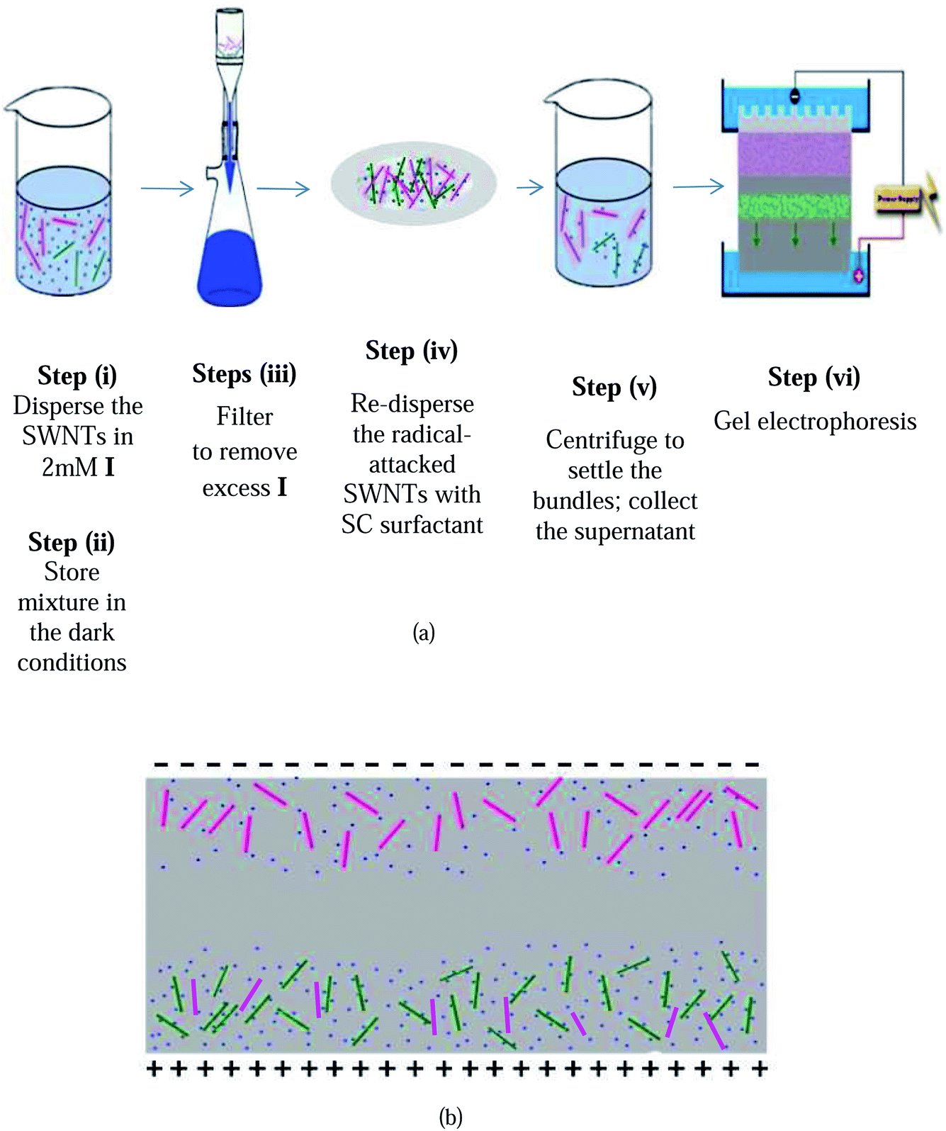 | ||
| Fig. 1 (a) Schematic representation of the separation procedure in the I-AGE method. (b) Schematic illustration of the separation mechanism in I-AGE. | ||
To the best of our knowledge, the present work is the first report of selective chemistry-assisted gel electrophoresis which achieves higher purity than previously proposed AGE techniques using SDS or CS-A. The enrichment was confirmed by UV-visible-Near Infrared spectroscopy (UV-vis-NIR) and Raman spectroscopy. The increased ratio of the D peak to the G peak (D/G) indicated by the Raman spectroscopy of the metallic-enriched eluted SWNTs obtained by AGE, confirms the functionalization and corroborates that the naphthyl-based radicals preferentially react with m-SWNTs. The enrichment of the s-SWNTs in the top fraction of the agarose gel was also confirmed by the high performance of network field effect transistors (FETs) fabricated using enriched nanotubes.
2. Results
During gel electrophoresis of the I-functionalized SC-dispersed P2 SWNTs (hereafter denoted “P2/SC-I”), some SWNTs migrated down the agarose gel while other SWNTs remained immobile in the top part of the gel. The nanotubes collected from the top gel fraction after AGE (hereafter denoted “P2/SC-I/AGE/Top”) and the nanotubes obtained from the bottom gel fraction (“P2/SC-I/AGE/Bottom”) were analyzed using UV-vis-NIR and Raman spectroscopy.Fig. 2a shows the UV-vis-NIR spectra of the semiconducting- and metallic-enriched SWNT fractions purified using the I-AGE technique. For P2 SWNTs, the first van Hove electronic transition of the metallic nanotubes (M11) and the second van Hove electronic transition of the semiconducting nanotubes (S22) occur in the 600–800 nm and 920–1050 nm ranges, respectively.32 For P2/SC-I/AGE/Top, which are semiconducting-enriched SWNTs, the M11 peak was decreased significantly compared to that of the un-separated pristine P2 samples (hereafter denoted “P2/Pristine”), confirming the reduced content of the metallic nanotubes after AGE. The purity of the semiconducting nanotubes obtained from the top gel fraction (pink curve) was estimated using the areas under the metallic M11 and semiconducting S22 bands to be about 98%, while that of the pristine P2 samples was estimated to be 78%. The significant reduction in the metallic content of the P2/SC-I/AGE/Top samples confirms the excellent selectivity of our combined functionalization cum AGE technique. The more reacted metallic nanotubes are postulated to move agilely towards the bottom electrode under the electric field. The bottom fraction (green curve, P2/SC-I/AGE/Bottom) is still dominated by semiconducting nanotubes, but is enriched (to about 30%) in metallic nanotube species compared with the input P2 SWNTs. To confirm the contribution of I functionalization in achieving good separation using AGE, a control AGE separation was also performed with non-I functionalized P2 SWNTs dispersed in 2% SC (denoted “P2/SC/AGE/Top”). As seen in Fig. 2a, this sample has only about 85% semiconducting purity in the top fraction, confirming the important role that I functionalization plays in achieving high purity semiconducting nanotubes through AGE.
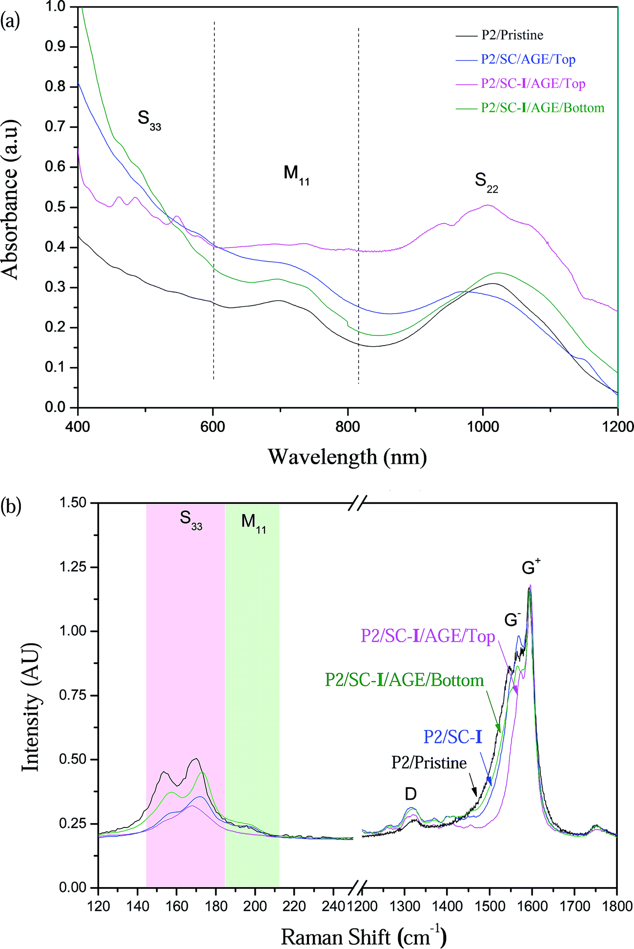 | ||
| Fig. 2 (a) UV-vis-NIR spectra of P2/Pristine, P2/SC/AGE and P2/SC-I after gel electrophoresis. (b) Raman spectra of P2/Pristine and P2/SC-I before and after gel electrophoresis, collected using a 633 nm laser. | ||
The separation efficiency of the proposed I-AGE technique was also examined using Raman spectroscopy. The radial breathing modes (RBM) of the two separated fractions (“top” and “bottom”) were measured with 633 nm Raman laser excitation, which excites both the metallic and semiconducting species of P2 SWNTs.3,33,34
Fig. 2b shows the Raman spectra with 633 nm excitation. The pristine P2 shows two major peaks at 155 cm−1 and 170 cm−1 due to the semiconducting species and one peak at 200 cm−1 due to the metallic species. The metallic peak is plainly present in the P2/Pristine sample (black curve) but is nearly absent from the P2/SC-I/AGE/Top curve (pink). The metallic peak of the P2/SC-I/AGE/Bottom samples (green curve) is enhanced relative to the semiconducting peaks. This corroborates the excellent enrichment of the semiconducting species in the top gel after I-AGE.
The G− band also confirms the reduction of the metallic nanotube species from the top fraction. For metallic nanotubes, due to the strong coupling in the density of states, the G− feature is broad and asymmetric while the G− band for the semiconducting nanotubes exhibits a Lorentzian line shape.3,35 As seen in Fig. 2b, the G− feature of the P2/SC-I/AGE/Top sample (at approximately 1550–1580 cm−1) is narrowed compared to those of the P2/SC-I/AGE/Bottom and pristine samples, corroborating the decreased metallic content in this fraction.
Raman spectroscopy was also used to verify the preferential covalent reaction of the I fragments with the metallic nanotubes. The ratio of the D peak to the G peak (D/G) is related to the extent of nanotube sidewall functionalization.12 As shown in Fig. 3 and Table 1, the D/G ratio was considerably higher for P2/SC-I/AGE/Bottom SWNTs than for the pristine sample or the P2/SC-I/AGE/Top fraction. This result confirms the higher extent of functionalization of the SWNTs in the bottom gel fraction, which is also the m-SWNT-enriched fraction. This corroborates with our previous finding that I-derived radicals preferentially attack metallic species, thereby enhancing their mobility under AGE compared with the less-attacked semiconducting species.
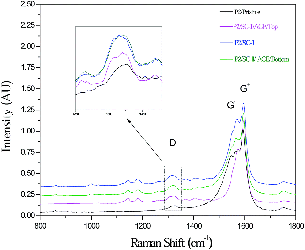 | ||
| Fig. 3 Raman spectra (633 nm) of the pristine and separated P2 SWNTs; inset is the enlarged view of the D-band evolution of the samples. | ||
| Sample | D/G ratio |
|---|---|
| P2/Pristine | 0.082 ± 0.021 |
| P2/SC-I | 0.149 ± 0.009 |
| P2/SC-I/AGE/Top | 0.098 ± 0.003 |
| P2/SC-I/AGE/Bottom | 0.146 ± 0.005 |
To demonstrate the suitability of the nanotubes separated by this method for use in electronic devices, the purified semiconducting SWNTs (P2/SC-I/AGE/Top) were applied in bottom-gated FETs using the dip coating technique (described in Section 4.4). For comparison purposes, a control sample of FETs (with a similar nanotube density) was fabricated using a P2/Pristine solution. A total of 20 FETs were fabricated using each of the above solutions.
Fig. 4a shows the variation of the drain current (Id) with gate voltage (Vgs) at a drain voltage (Vds) of 1.5 V, for a representative device fabricated using a P2/SC-I/AGE/Top solution. This FET shows typical p-type transistor characteristics and a carrier mobility of 6.7 cm2 V−1 s−1. Fig. 4b shows the variation in the output characteristic drain current (Id) with the drain voltage (Vd), measured at several gate voltages over the range −150 to 150 V. Fig. 4c shows the histogram of the on/off ratios of the 20 FETs fabricated using purified semiconducting SWNTs as well as that of 20 FETs made using the un-separated pristine P2 solution (with similar nanotube densities). The FETs fabricated using the P2/SC-I/AGE/Top solution exhibit significantly higher on/off ratios (predominantly ≥ 104) than the FETs made with the P2/Pristine solution (on/off ratios mostly < 102). Fig. 4d shows the trend of the on/off ratio with mobility for the devices fabricated using the purified semiconducting SWNTs (P2/SC-I/AGE/Top). The FETs fabricated using our enriched semiconducting SWNTs show promising performance metrics: on/off ratios ranging from 102 to 106 and mobilities ranging from 3.6 to 11.7 cm2 V−1 s−1. These metrics are significantly higher than those of the devices fabricated using un-separated nanotubes.
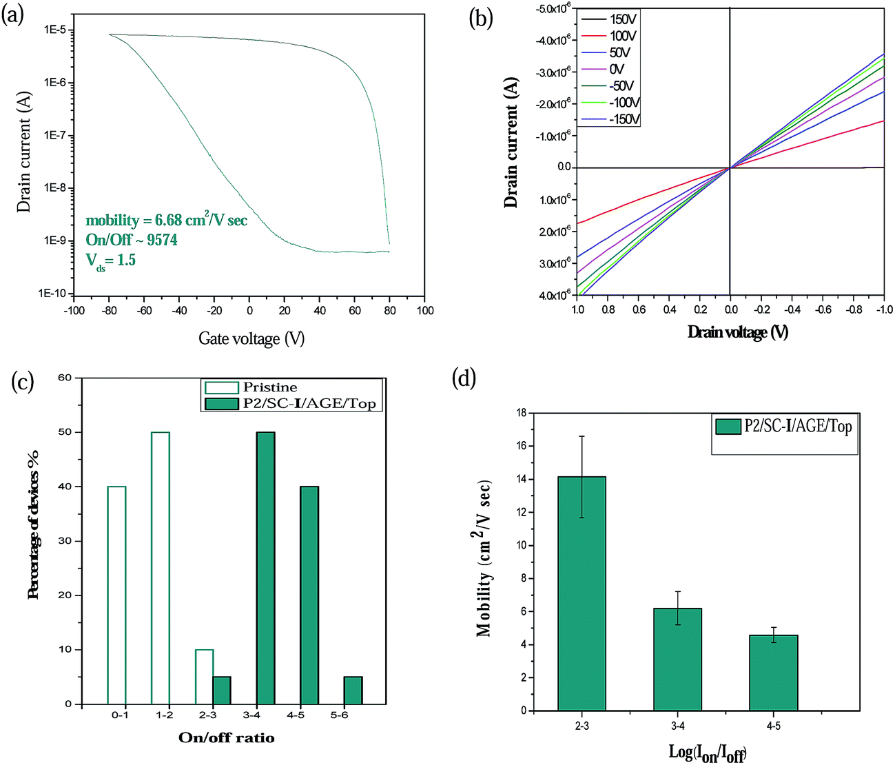 | ||
| Fig. 4 (a) Transfer characteristics (Vds = 1.5 V) of Idsvs. Vgs for bottom-gated FETs fabricated using the P2/SC-I/AGE/Top solution. (b) Output characteristics, Idsvs. Vds, measured at gate voltages of 150 (top) to −150 V (bottom) with 50 V intervals. (c) Histogram of on/off ratios of 20 devices made with P2/SC-I/AGE/Top SWNTs (blue) and 20 devices made with pristine SWNTs (white). (d) The trend of the on/off ratio with device mobility for the devices fabricated using the P2/SC-I/AGE/Top solution. | ||
Fig. 5a shows the morphology of the nanotube network as measured by AFM. The device channel area is observed to be covered by a film-like layer of SWNTs with an estimated density of ∼20 tubes per μm2. The length distribution of nanotubes after I-AGE is shown in Fig. 5b. The average length of nanotubes after enrichment with I-AGE was estimated to be about 0.5 μm, indicating some shortening of the nanotubes after enrichment (length of pristine SWNTs = ∼1 μm). The shortening of the nanotubes in I-AGE is mainly due to the long sonication duration (3 h) required to prepare samples for I-AGE.
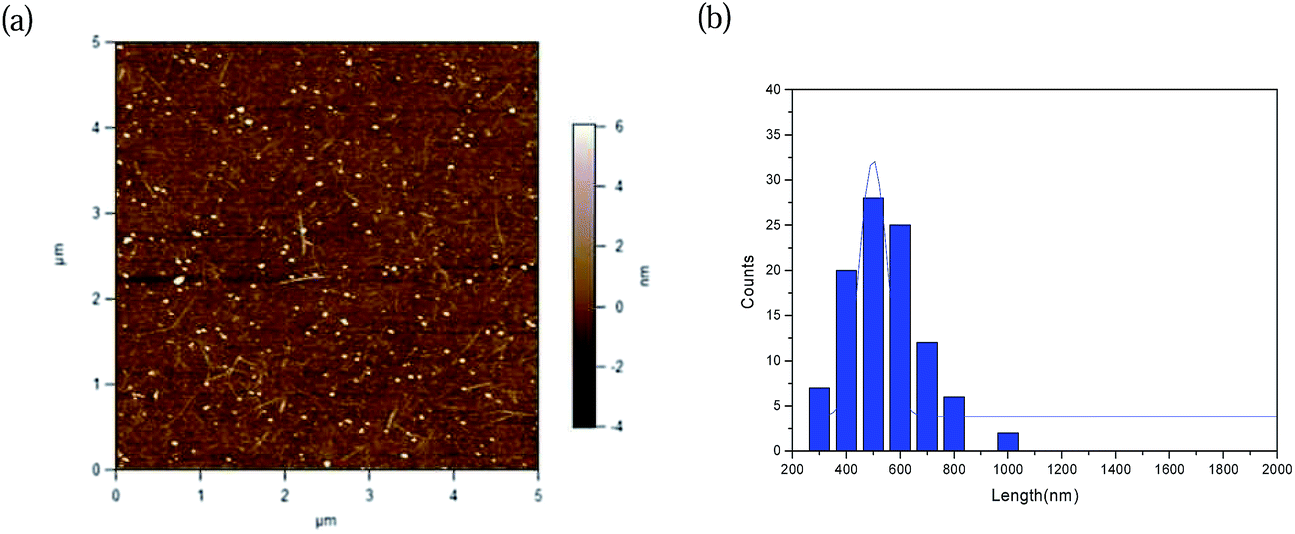 | ||
| Fig. 5 (a) Atomic force microscopy (AFM) image of a representative FET fabricated using the P2/SC-I/AGE/Top solution. (b) Length distribution of the P2/SC-I/AGE/Top SWNTs. | ||
The results of the UV-vis-NIR and Raman spectroscopy, and the performance of the FETs presented above confirm the excellent separation of the metallic from the semiconducting nanotubes using our proposed I-AGE technique. The process yield of our I-AGE technique based on the original nanotube input was measured to be about 18%, which is significantly higher than the yield of other highly selective techniques such as I-DGU (<5%).29 The simultaneous high selectivity with high yield of the proposed technique makes it appealing for industrial scale production of high purity semiconducting nanotubes.
The promising separation achieved using this I-AGE technique originates from the unique characteristics of I, including its capability to generate radicals which preferentially attack unwanted metallic species and its relatively high charge density.29 Due to the relatively high negative charge of I and the preferential radical reactivity with metallic nanotubes, a significant differential charge density develops between the reacted nanotubes, which contain most of the metallic species as well as many of the semiconducting species, and the unreacted nanotubes, which are almost entirely semiconducting. In the presence of an applied electric field, non-covalently bound I molecules are likely to be stripped from the nanotube surfaces so that the s-SWNTs, which are non-covalently functionalized with undecomposed I molecules, will be relatively immobile. The significantly higher charge of the reacted nanotubes compared to the unreacted ones, results in considerable differential electrophoretic mobility between the two populations under a uniform electric field during AGE. The more mobile negatively charged fraction, which is enriched in metallic species, moves towards the anode electrode. The less charged fraction, which is highly depleted in metallic species, remains in the upper portion of the gel. Based on the results presented here and the results of previous studies using CS-A and SDS,30,31 we hypothesize that achieving good separation with AGE requires (i) the use of highly charged dispersants/functionalization agents to increase the mobility of the SWNTs under an electric field and (ii) the selectivity of the charged dispersing/functionalization agents for metallic or semiconducting nanotubes, leading to the development of differential mobility between the two species. The higher purity achieved using I rather than CS-A, despite both having relatively similar charge densities,29,31 indicates that while a high charge density of the dispersing/functionalization agent is a requirement of separation, the key to achieving higher purities with AGE is to increase the selectivity of the charged dispersing/functionalization agents for metallic or semiconducting nanotubes.
Due to its relatively high selectivity, process yield and throughput, the method developed in this study has great potential for scaling and commercialization. However, industrial scale up of this method requires further investigation into the potential effects that increasing the throughput may have on purity and yield of the semiconducting SWNTs produced. In addition, the commercialization potential of this method may be increased by shortening the process duration of the various steps involved including AGE, acid treatment and selective functionalization.
3. Conclusions
We have shown that sonication of a novel naphthalene-based azo compound prior to dispersing the mixture with sodium cholate and then subjecting the mix to AGE can separate most of the metallic nanotubes from the immobile nanotubes, considerably increasing the semiconducting purity of these SWNTs. The higher s-SWNT purity achievable using our proposed technique compared to previously proposed AGE techniques using SDS and CS-A, confirms the effect of the I-radicals on separation. The high process yield (∼18%) and high purity (∼98%) achieved when using our proposed technique, together with its affordability and scalability, render it highly appealing for industrial scaling. Network FET devices made with the semi-enriched SWNTs show promising performance metrics (mobility in the range of ∼3.6 to 11.7 cm2 V−1 s−1 and on/off ratios from 102 to 106). The efficiency of our proposed I-AGE technique originates mainly from the preferential reactivity of the radicals of I with metallic nanotubes as well as the relatively high charge density of these radicals.4. Experimental section
4.1. Materials
Direct Blue 71 (I), sodium cholate (SC), sodium dodecyl sulphate (SDS), boric acid, tris hydroxymethyl aminomethane, dimethylformamide (DMF) and nitric acid were purchased from Sigma-Aldrich (Singapore) and used as received. Purified arc discharge SWNTs (P2) were purchased from Carbon Solutions, Inc. (Riverside, CA, USA). Agarose was purchased from NacalaiTesque (Japan).4.2. Solution preparation and selective functionalization
15 mg of purified arc discharge (P2) nanotubes were mixed with 2 mM of Direct Blue 71 in 50 ml deionized water. The solution was stirred for 45 min at 60 °C and was probe-sonicated (SONICS, VCX-130) in an ice bath for 3 h (70% amplitude, 5 s on, 2 s off). The solution was stored in the dark for 48 h and was subsequently filtered and then washed with water two to three times to remove any unreacted I. The reacted SWNT powder was re-dispersed in an aqueous solution containing 2 wt% of sodium cholate and was centrifuged (Sartorius, SIGMA@3K30) at 50![[thin space (1/6-em)]](https://www.rsc.org/images/entities/char_2009.gif) 000g for 1 h to settle the SWNT bundles. The supernatant was collected for further purification using agarose gel electrophoresis.
000g for 1 h to settle the SWNT bundles. The supernatant was collected for further purification using agarose gel electrophoresis.
4.3. Gel electrophoresis
1 wt% agarose was added to 0.2 wt% surfactant in a 2× transport buffer (TB) solution (pH = 8.5; 48.5 mM boric acid and 50 mM tris hydroxymethyl aminomethane). The agarose gel solution was then melted in a microwave oven and used to fill the gel container (0.3 cm × 20 cm × 20 cm plate container) of the gel electrophoresis apparatus (PROTEAN II XI, Bio Rad Laboratories, Singapore) up to about 2/3 of its height. Subsequently, 20 ml of the functionalized SWNT solution, prepared as described in Section 4.2, was mixed with a similar volume (20 ml) of 2 wt% agarose solution and used to fill the remaining 1/3 space of the plate container, after being melted in a microwave oven. The gel electrophoresis apparatus was then run at 200 V for 4 h. After AGE, the gel was cut into three fractions distinguished by differences in color.31,36 The top and bottom gel fractions containing the purified semiconducting and metallic-enriched SWNTs, respectively, were degraded in 10% nitric acid at 80 °C for 18 h followed by a basic wash (1 M NaOH) to remove the agarose gel. The purified SWNTs were washed twice with distilled water and sonicated in DMF solvent three times to remove I. They were then redispersed in a (1:4) mixture of SDS and SC solution using probe sonication (Sonics, 130 W, 20 kHz). After probe sonication, the SWNT solution was centrifuged at 50000g for 1 h and the supernatant was then collected and used for characterization and, in the case of the s-SWNTs, for fabrication of field effect transistors. The s-SWNTs were annealed after acid and base treatments. Annealing was performed in argon for 1 h at 400 °C.
4.4. Characterization
The clean SWNTs obtained from the top and bottom gel fractions were examined by UV-vis-NIR and Raman spectroscopy. UV-vis-NIR spectroscopy was performed using a Varian Cary 5000 UV-vis-NIR spectrophotometer. Raman spectroscopy was conducted using a Renishaw inVia Raman microscope equipped with a 633 nm (1.96 eV) laser. The purity of the semiconducting nanotubes obtained through I-AGE was estimated using the AS/(AM + AS) ratio, where AS and AM are respectively, the areas under the semiconducting (S22) and metallic (M11) absorption spectral bands in the UV-vis-NIR spectra, after baseline subtraction.The semiconducting SWNTs obtained from the top gel fraction were used to fabricate field effect transistors (FETs) using the dip coating method. All devices were fabricated on silicon substrates covered with a 300 nm thick SiO2 layer which served as the gate dielectric. The surface of the substrate was cleaned with piranha solution and, prior to nanotube deposition, was functionalized with aminopropyltriethoxysilane (APTES) to improve the uniformity of the nanotube network.37 To create networks of nanotubes, the wafer was repeatedly immersed into the purified s-SWNT solution until sufficient nanotube density was deposited on the wafer. The wafer was then rinsed with deionized water to completely remove the surfactants and was dried with nitrogen gas. The wafers were then annealed in argon for 1 h at 400 °C and later in vacuum at 250 °C for 2 h. After annealing, source and drain gold electrodes were deposited on the substrate by photolithography and the active channel regions were then covered with a protective passivation layer. After depositing the protective layer, the remaining unprotected SWNTs outside the FET channel were etched away by oxygen plasma (100 W, 2 min). The FET channel width and length were 50 and 100 μm, respectively. The nanotube network morphology was measured by atomic force microscopy (AFM) with a MFP 3D microscope (Asylum Research) in AC mode.
A Keithley semiconductor parameter analyzer Model 4200-SCS was used to characterize the FET performance. The mobility was estimated using the following well-known equation:38
 | (1) |
 | (2) |
Acknowledgements
This work was supported by a Competitive Research Program grant from the Singapore National Research Foundation (NRF-CRP2-2007-02) and an ASTAR grant (102 170 0141). Sara Mesgari acknowledges the support of Nanyang Technological University through a Research Scholarship.References
- J. Liu and M. C. Hersam, Recent developments in carbon nanotube sorting and selective growth, MRS Bull., 2010, 35(4), 315–321 CrossRef CAS.
- M. C. Hersam, Progress towards monodisperse single-walled carbon nanotubes, Nat. Nanotechnol., 2008, 3(7), 387–394 CrossRef CAS PubMed.
- C. H. Liu and H. L. Zhang, Chemical approaches towards single-species single-walled carbon nanotubes, Nanoscale, 2010, 2(10), 1901–1918 RSC.
- S. A. Hodge, et al., Unweaving the rainbow: A review of the relationship between single-walled carbon nanotube molecular structures and their chemical reactivity, Chem. Soc. Rev., 2012, 41(12), 4409–4429 RSC.
- H. Park, et al., High-density integration of carbon nanotubes via chemical self-assembly, Nat. Nanotechnol., 2012, 7(12), 787–791 CrossRef CAS PubMed.
- Y. Maeda, et al., Large-scale separation of metallic and semiconducting single-walled carbon nanotubes, J. Am. Chem. Soc., 2005, 127(29), 10287–10290 CrossRef CAS PubMed.
- Y. Maeda, et al., Dispersion and separation of small-diameter single-walled carbon nanotubes, J. Am. Chem. Soc., 2006, 128(37), 12239–12242 CrossRef CAS PubMed.
- R. Voggu, et al., A simple method of separating metallic and semiconducting single-walled carbon nanotubes based on molecular charge transfer, J. Am. Chem. Soc., 2010, 132(16), 5560–5561 CrossRef CAS PubMed.
- P. Anilkumar, et al., Non-covalent interactions of derivatized pyrenes with metallic and semiconducting single-walled carbon nanotubes, J. Phys. Chem. C, 2011, 115(22), 11010–11015 CAS.
- H. P. Li, et al., Selective interactions of porphyrins with semiconducting single-walled carbon nanotubes, J. Am. Chem. Soc., 2004, 126(4), 1014–1015 CrossRef CAS PubMed.
- W. J. Kim, M. L. Usrey and M. S. Strano, Selective functionalization and free solution electrophoresis of single-walled carbon nanotubes: Separate enrichment of metallic and semiconducting SWNT., Chem. Mater., 2007, 19(7), 1571–1576 CrossRef CAS.
- M. S. Strano, et al., Electronic structure control of single-walled carbon nanotube functionalization, Science, 2003, 301(5639), 1519–1522 CrossRef CAS PubMed.
- W. J. Kim, et al., Connecting Single Molecule Electrical Measurements to Ensemble Spectroscopic Properties for Quantification of Single-Walled Carbon Nanotube Separation, J. Am. Chem. Soc., 2009, 131(9), 3128–3129 CrossRef CAS PubMed.
- H. Hu, et al., Sidewall Functionalization of Single-Walled Carbon Nanotubes by Addition of Dichlorocarbene, J. Am. Chem. Soc., 2003, 125(48), 14893–14900 CrossRef CAS PubMed.
- K. H. An, et al., A diameter-selective attack of metallic carbon nanotubes by nitronium ions, J. Am. Chem. Soc., 2005, 127(14), 5196–5203 CrossRef CAS PubMed.
- C. M. Yang, et al., Selective removal of metallic single-walled carbon nanotubes with small diameters by using nitric and sulfuric acids, J. Phys. Chem. B, 2005, 109(41), 19242–19248 CrossRef CAS PubMed.
- K. H. An, et al., A diameter-selective chiral separation of single-wall carbon nanotubes using nitronium ions, J. Electron. Mater., 2006, 35(2), 235–242 CrossRef CAS.
- M. Yudasaka, M. Zhang and S. Iijima, Diameter-selective removal of single-wall carbon nanotubes through light-assisted oxidation, Chem. Phys. Lett., 2003, 374(1–2), 132–136 CrossRef CAS.
- Y. Miyata, Y. Maniwa and H. Kataura, Selective oxidation of semiconducting single-wall carbon nanotubes by hydrogen peroxide, J. Phys. Chem. B, 2006, 110(1), 25–29 CrossRef CAS PubMed.
- C. Ménard-Moyon, et al., Separation of semiconducting from metallic carbon nanotubes by selective functionalization with azomethine ylides, J. Am. Chem. Soc., 2006, 128(20), 6552–6553 CrossRef PubMed.
- G. Schmidt, et al., Labile diazo chemistry for efficient silencing of metallic carbon nanotubes, Chem. – Eur. J., 2011, 17(5), 1415–1418 CrossRef CAS PubMed.
- G. Schmidt, et al., Mechanism of the Coupling of Diazonium to Single-Walled Carbon Nanotubes and Its Consequences, Chem. – Eur. J., 2009, 15(9), 2101–2110 CrossRef CAS PubMed.
- M. L. Usrey, E. S. Lippmann and M. S. Strano, Evidence for a two-step mechanism in electronically selective single-walled carbon nanotube reactions, J. Am. Chem. Soc., 2005, 127(46), 16129–16135 CrossRef CAS PubMed.
- Z. Dai, et al., Selective Small-Diameter Metallic Single-Walled Carbon Nanotube Removal by Mere Standing with Anthraquinone and Application to a Field-Effect Transistor, J. Phys. Chem. C, 2010, 114(49), 21035–21041 CAS.
- J. B. Li, et al., On-chip diameter-dependent conversion of metallic to semiconducting single-walled carbon nanotubes by immersion in 2-ethylanthraquinone, RSC Adv., 2012, 2(4), 1275–1281 RSC.
- J. W. Zhao, et al., Solution-processable semiconducting thin-film transistors using single-walled carbon nanotubes chemically modified by organic radical initiators, Chem. Commun., 2009, 7182–7184 RSC.
- C. W. Lee, et al., Solution-processable carbon nanotubes for semiconducting thin-film transistor devices, Adv. Mater., 2010, 22(11), 1278–1282 CrossRef CAS PubMed.
- J. Lu,
et al., Selective Interaction of Large or Charge-Transfer Aromatic Molecules with Metallic Single-Wall Carbon Nanotubes: Critical Role of the Molecular Size and Orientation, J. Am. Chem. Soc., 2006, 128(15), 5114–5118 CrossRef CAS PubMed.
- A. K. Sundramoorthy, et al., Scalable and effective enrichment of semiconducting single-walled carbon nanotubes by a dual selective naphthalene-based AzO dispersant, J. Am. Chem. Soc., 2013, 135(15), 5569–5581 CrossRef CAS PubMed.
- T. Tanaka, et al., High-yield separation of metallic and semiconducting single-wall carbon nanotubes by agarose gel electrophoresis, Appl. Phys. Express, 2008, 1(11), 1140011–1140013 Search PubMed.
- S. Mesgari, et al., High Selectivity cum Yield Gel Electrophoresis Separation of Single-Walled Carbon Nanotubes Using a Chemically Selective Polymer Dispersant, J. Phys. Chem. C, 2012, 116(18), 10266–10273 CAS.
- M. J. O'Connell, et al., Band gap fluorescence from individual single-walled carbon nanotubes, Science, 2002, 297(5581), 593–596 CrossRef PubMed.
- M. C. LeMieux, et al., Self-sorted, aligned nanotube networks for thin-film transistors, Science, 2008, 321(5885), 101–104 CrossRef CAS PubMed.
- N. Anderson, A. Hartschuh and L. Novotny, Chirality changes in carbon nanotubes studied with near-field Raman spectroscopy, Nano Lett., 2007, 7(3), 577–582 CrossRef CAS PubMed.
- S. M. Keogh, et al., Spectroscopic analysis of single-walled carbon nanotubes and semiconjugated polymer composites, J. Phys. Chem. B, 2004, 108(20), 6233–6241 CrossRef CAS PubMed.
- S. Mesgari, et al., Polymer removal from electronic grade single-walled carbon nanotubes after gel electrophoresis, J. Mater. Chem. C, 2013, 1(41), 6813–6823 RSC.
- D. Chattopadhyay, I. Galeska and F. Papadimitrakopoulos, A route for bulk separation of semiconducting from metallic single-wall carbon nanotubes, J. Am. Chem. Soc., 2003, 125(11), 3370–3375 CrossRef CAS PubMed.
- C. Wang, et al., Wafer-scale fabrication of separated carbon nanotube thin-film transistors for display applications, Nano Lett., 2009, 9(12), 4285–4291 CrossRef CAS PubMed.
- Q. Cao, et al., Gate capacitance coupling of singled-walled carbon nanotube thin-film transistors, Appl. Phys. Lett., 2007, 90(2), 023516-1–023516-3 CrossRef PubMed.
| This journal is © The Royal Society of Chemistry 2014 |