 Open Access Article
 This Open Access Article is licensed under a
 Creative Commons Attribution 3.0 Unported Licence
Single-walled carbon nanotube networks in conductive composite materials
Oana A.
Bârsan
*ab,
Günter G.
Hoffmann
ab,
Leo G. J.
van der Ven
ac and
G. (Bert)
de With
a
aLaboratory of Materials and Interface Chemistry, Eindhoven University of Technology, Den Dolech 2 5612 AZ, Eindhoven, the Netherlands. E-mail: O.A.Barsan@tue.nl
bDutch Polymer Institute (DPI), P.O. Box 902, 5600 AX, Eindhoven, the Netherlands. E-mail: info@polymers.nl; Fax: +31 40 247 24 62; Tel: +31 40 247 56 29
cAkzo Nobel Automotive & Aerospace Coatings, Sassenheim, the Netherlands
First published on 29th May 2014
Abstract
Electrically conductive composite materials can be used for a wide range of applications because they combine the advantages of a specific polymeric material (e.g., thermal and mechanical properties) with the electrical properties of conductive filler particles. However, the overall electrical behaviour of these composite materials is usually much below the potential of the conductive fillers, mainly because by mixing two different components, new interfaces and interphases are created, changing the properties and behaviours of both. Our goal is to characterize and understand the nature and influence of these interfaces on the electrical properties of composite materials. We have improved a technique based on the use of sodium carboxymethyl cellulose (CMC) to disperse single-walled carbon nanotubes (SWCNTs) in water, followed by coating glass substrates, and drying and removing the CMC with a nitric acid treatment. We used electron microscopy and atomic force microscopy techniques to characterize the SWCNT films, and developed an in situ resistance measurement technique to analyse the influence of both the individual components and the mixture of an epoxy/amine system on the electrical behaviour of the SWCNTs. The results showed that impregnating a SWCNT network with a polymer is not the only factor that affects the film resistance; air exposure, temperature, physical and chemical properties of the individual polymer components, and also the formation of a polymeric network, can all have an influence on the macroscopic electrical properties of the initial SWCNT network. These results emphasize the importance of understanding the effects that each of the components can have on each other before trying to prepare an efficient polymer composite material.
Introduction
The potential of carbon nanotubes (CNTs) in many different fields has led to an exponential growth of interest in these materials over the past twenty years.1 Not only their structure and size, but also their excellent mechanical, thermal, optical and electrical properties have widened the range of applications and scientific fields in which there has been an increased interest in understanding and exploiting them.2–6 Single-walled carbon nanotubes (SWCNTs) in particular are gaining popularity due to their large aspect ratios, narrow diameter distribution, semiconductor properties and also their increasing availability on the market. These materials have been used to prepare thin conductive and transparent films,7–9 and also electrically conductive,10 mechanically reinforced11 or thermally conductive12 polymer composites. Because SWCNTs exert strong van der Waals attractive forces, they are very difficult to disperse without the use of surfactants or other dispersion agents.13–16 Functionalization has proved to be efficient in increasing SWCNT dispersibility in different solvents or polymers.17,18 However, the process involves damaging the surface of the SWCNTs, which in turn affects their mechanical and electrical properties. Despite their potential and the numerous studies on SWCNTs, there are many unresolved issues when practical applications, such as electrically conductive composites, are concerned. These materials have not yet surpassed the efficiency of existing composite materials such as graphite or metal fiber/flake reinforced polymers.19,20Electrically conductive composites are typically prepared by dispersing SWCNTs, directly or with the aid of solvents, into a polymer.10,21 This approach has led to the preparation of inhomogeneous composites with poorly dispersed SWCNTs and low conductivity values, even though percolation thresholds as low as 0.001 wt% have been achieved.10,21–23 On the one hand, in order to obtain a good and stable dispersion of SWCNTs in a polymer, good compatibility between the two components is necessary. On the other hand, surrounding the conductive particles with an insulating polymer layer leads to individually insulated SWCNTs, dispersed throughout the polymer matrix. Such composites would either be insulators or have very low conductivities. This means that the contacts between the conductive particles inside a polymer matrix play a crucial role in the electrical properties of composite materials. Having a uniform SWCNT network, with good physical and electrical contacts within a polymer matrix, is a factor required for achieving good conductivities in composite materials.
Recently, a different approach was successfully used to obtain SWCNT/polymer composite thin films24 with sheet resistance (RS) values in the range of 100–1000 ohm sq−1. This technique involves two main steps: (1) preparing a uniform SWCNT thin film on a glass substrate; (2) coating the SWCNT film with a specific polymer followed by drying/curing the polymer and peeling the film off the glass substrate. A free-standing composite film is obtained in this way. This approach brings the advantages of first having a SWCNT network with good physical and electrical properties, and then filling the gaps with the desired polymer. The idea is particularly appealing since it ensures good physical and electrical contacts between the SWCNTs, and allows a proper characterization of the network's properties before actually adding the polymer matrix. However, the influence of the newly formed interfaces on the electrical properties of the polymer impregnated SWCNT network has not been studied in detail. We have adapted and improved the technique and designed a method for directly measuring and characterizing the influence of the polymer matrix on the SWCNT network. The purpose of our study is to analyze how the polymeric network affects the electrical behaviour of the already existing SWCNT network.
Experimental
SWCNT film preparation
All chemicals were used as received, without any further purification. Super high purity SWCNTs manufactured by the CVD method were purchased from US Research Nanomaterials, Inc. 0.1% solutions of SWCNTs were prepared by adding 10 mg SWCNTs as purchased and 300 mg of sodium carboxymethyl cellulose (CMC), 90![[thin space (1/6-em)]](https://www.rsc.org/images/entities/char_2009.gif) 000 MW (C28H30Na8O27), from Sigma Aldrich to 10 mL of distilled water. The solutions were kept cool in an ice bath while being sonicated for 15 minutes using a SONICS Vibra-Cell sonicator with a 6.4 mm tip diameter and 60% amplitude (as described by Li et al.24). The solution was then centrifuged at 8500 rpm for 1 hour in a 1.5 cm diameter vessel, using a SIGMA 3-30K centrifuge and only the upper 80% of the supernatant was kept. The glass substrates were cleaned by immersion into a RCA cleaning solution (5 parts H2O, 1 part NH4OH, 30%, 1 part H2O2, 30%) without heating, left overnight and then rinsed with distilled water. Thin SWCNTs + CMC films were deposited on 7 cm × 7 cm glass substrates with a 30 μm gap doctor blade at a speed of 10 mm s−1, using a COATMASTER 509 MC. The films were then dried for 20 h in an oven at 45 °C. The as-prepared samples were immersed into an acid bath (HNO3, 9 M) for 4 hours at 40 °C, and thereafter taken out and dried at 45 °C for 2 hours under vacuum. The samples were subsequently kept for 20 h at 150 °C under vacuum for acid residue removal, and for two hours at 400 °C in a nitrogen atmosphere for CMC residue removal. Thermogravimetric analysis (TGA) on pure CMC was performed using Q500 equipment, with a heating rate of 10 °C per minute between 25–600 °C both in air and nitrogen atmospheres.
000 MW (C28H30Na8O27), from Sigma Aldrich to 10 mL of distilled water. The solutions were kept cool in an ice bath while being sonicated for 15 minutes using a SONICS Vibra-Cell sonicator with a 6.4 mm tip diameter and 60% amplitude (as described by Li et al.24). The solution was then centrifuged at 8500 rpm for 1 hour in a 1.5 cm diameter vessel, using a SIGMA 3-30K centrifuge and only the upper 80% of the supernatant was kept. The glass substrates were cleaned by immersion into a RCA cleaning solution (5 parts H2O, 1 part NH4OH, 30%, 1 part H2O2, 30%) without heating, left overnight and then rinsed with distilled water. Thin SWCNTs + CMC films were deposited on 7 cm × 7 cm glass substrates with a 30 μm gap doctor blade at a speed of 10 mm s−1, using a COATMASTER 509 MC. The films were then dried for 20 h in an oven at 45 °C. The as-prepared samples were immersed into an acid bath (HNO3, 9 M) for 4 hours at 40 °C, and thereafter taken out and dried at 45 °C for 2 hours under vacuum. The samples were subsequently kept for 20 h at 150 °C under vacuum for acid residue removal, and for two hours at 400 °C in a nitrogen atmosphere for CMC residue removal. Thermogravimetric analysis (TGA) on pure CMC was performed using Q500 equipment, with a heating rate of 10 °C per minute between 25–600 °C both in air and nitrogen atmospheres.
SWCNT film characterization
Sheet resistance measurements were performed using standard four point probe measurements with a 4 mm probe spacing. A Keithley electrometer model 6517A and source-meter model 237 were used to apply current and measure the resulting voltage drop. The results were converted to sheet resistance using correction factors for rectangular thin films as shown by Smits et al.25 Scanning electron microscopy (SEM) images were taken with a Quanta 3D FEG microscope and scanning transmission electron microscopy (STEM) images were acquired using a Titan electron microscope operated at 300 kV with a High Angle Annular Dark Field (HAADF) detector. Atomic force microscopy (AFM) was performed using a SOLVER NEXT in tapping mode, and a Veeco 150 Dektak profilometer (Bruker) was used for thickness measurements. Raman spectra were taken with a LabRAM confocal spectrometer (Horiba Scientific) with an excitation wavelength of 632 nm. Transmittance measurements were performed using a SHIMADZU UV-3102 PC spectrophotometer in the range of 350–700 nm.Polymer impregnation
An epoxy/amine system was used as the polymer matrix. A bisphenol A based epoxy resin (Epikote 828, Resolution Nederland BV) with an equivalent weight (eqw) per epoxide group of 187 g mol−1, and Jeffamine D-230 (Huntsman Holland BV) with an NH-eqw of 60 g mol−1 were chosen as the model system. The polymer was prepared by mixing the two components at a 1:1 epoxy/amine ratio (based on an epoxy group/NH equivalent), using a RCT basic IKA magnetic stirrer for 5 minutes at 700 rpm for 5 minutes, followed by 3 minutes degassing in a BRANSON 1510 ultrasonic cleaner. The mixture was then coated onto the SWCNT film using a 60 μm gap doctor blade, and cured in an oven at 100 °C for 4 hours. Contact angle measurements on the SWCNT films were performed at room temperature using an OCA 30 System.
In situ resistance measurements
The previously prepared 7 cm × 7 cm SWCNT films on glass substrates were cut to sample sizes of 2 cm × 3.5 cm. An EMITECH K550 sputter coater at a current of 20 mA was used to deposit two 1 cm wide gold electrodes on each sample, leaving a 1.5 cm uncovered strip across the width of the samples (example in Fig. 6). A VOLTCRAFT VC840 multimeter was connected to the gold electrodes and a computer to enable in situ resistance measurements on each sample to be performed. The polymer was manually applied on the uncovered area of the SWCNT film while the resistance was being measured.Results and discussion
SWCNT film preparation and characterization
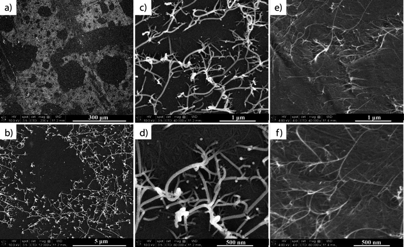
In the first part of our research, SWCNT films were prepared using a technique adapted from Li et al.,24 from a water solution of SWCNTs dispersed with CMC. The water was then removed by drying in an oven while the CMC was removed by nitric acid treatment, followed by several temperature treatments (45 °C, 150 °C and 400 °C) for the subsequent removal of acid and CMC residues. The prepared films (see the experimental section) were characterized by SEM and TEM after each step of the process to ensure the complete removal of CMC residues, and the nanometer and micrometer scale homogeneity of the SWCNT films. The majority of the CMC from the films was removed after the acid treatment. However, islands of CMC residue and also structures similar to polymer wrapping of SWCNTs26–28 were visible under SEM and TEM measurements, respectively (Fig. 1b, c and e). Because the TGA results showed that CMC degrades between 250–300 °C, the samples were also subjected to a 400 °C final thermal treatment, during which the remaining CMC residue was fully removed (Fig. 1d and f).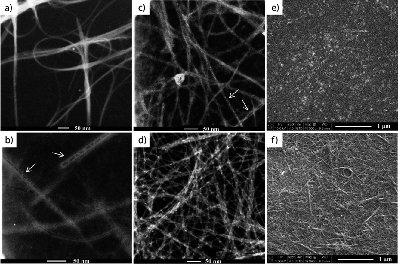 | ||
| Fig. 1 TEM images of (a) as-purchased SWCNTs, (b) SWCNTs + CMC film, and TEM and SEM images of the same SWCNT film after nitric acid treatment (c and e) and after the final 400 °C thermal treatment (d and f), respectively. | ||
The samples were also subjected to four-point probe measurements after each of the thermal treatment steps to monitor the evolution of the films' sheet resistance. After drying at 45 °C and 150 °C all of the films had a sheet resistance (RS) of RS = 200–250 ohm sq−1 and 300–500 ohm sq−1, respectively, suggesting that the water and nitric acid were gradually removed from the films. The final 400 °C treatment of the films led to a sheet resistance of RS = 1000–1500 ohm sq−1. This last step had the double purpose of removing the remaining CMC residue from the network but also of removing the p-type doping effect29 of the remaining nitric acid adsorbed into the SWCNT network.
Raman spectra taken of the pristine SWCNTs and the films after the final thermal treatment show an increase in the intensity of the D-band, generally associated with the amount of defects in SWCNTs30–32 (Fig. 2), when compared to the intensity of the G-band. The IG/ID ratio drops from 27 for the pristine material to 16 for the treated SWCNTs, which could be due to a shortening of the tubes during ultrasonication, or the introduction of some defects during the nitric acid treatment. Even if some damage occurred to the SWCNTs during the preparation procedures, the quality of the materials remained high.33,34
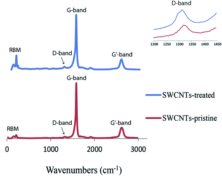 | ||
| Fig. 2 Raman spectra of the SWCNTs as purchased and after film preparation. | ||
The thickness of the films was determined by scratching the films and measuring the height profile across the scratch with a profilometer. Even if the initial SWCNTs + CMC films had thicknesses of approximately 500 nm, after removing the CMC they were reduced to 20–40 nm (Fig. 3a and b). AFM measurements were consistent with the profilometer measurements and showed a cross-section roughness of approximately 40 nm (Fig. 3c–e). AFM, SEM and profilometer measurements all revealed a uniformly dispersed SWCNT network with several large ropes of entangled SWCNTs at the surface. These ropes at as high as 100 nm formed at the surface of the films, most likely during the acid treatment where the tubes at the surface had the freedom to rearrange themselves into a more stable configuration.
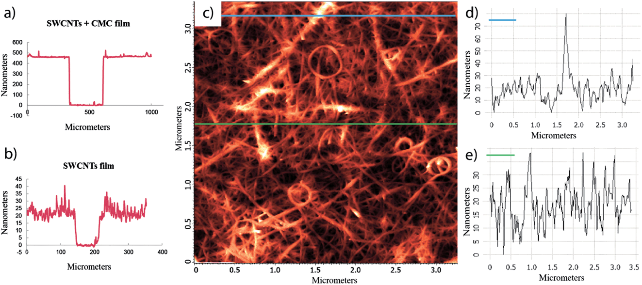 | ||
| Fig. 3 Profilometer height profile across a scratch in (a) a SWCNTs + CMC film and (b) a SWCNT film. AFM topography image of (c) a SWCNT film and (d and e) cross-section roughness profiles. | ||
Polymer impregnation
The second part of our research focused on impregnating the SWCNTs with a polymer. Li et al.24 used the SWCNT films to deposit a layer of polymer on top of the films, and after drying or curing, peeling-off the films from the glass substrates. Assuming that the polymer fully penetrated the SWCNT network, the free standing film obtained contained a SWCNT network embedded on one side of the polymer film. For most of the polymers they tested, the free-standing films had an up to 10 times lower sheet resistance on the bottom side of the film.We focused on impregnating the SWCNTs with an epoxy/amine polymer system (Epikote 828 and Jeffamine D-230 (ref. 35)). Droplets of the epoxy/amine uncured mixture and the individual components were added onto the SWCNT film to determine whether the polymers had sufficient compatibility with the SWCNTs to fully impregnate the film. Contact angle measurements showed that even if the epoxy resin had a contact angle of 97.4°, the polymer mixture (75.7 wt% epoxy resin) had a contact angle of 30.2°, which is much closer to the value of the amine alone of 14.7° (Fig. 4). The fact that the contact angle of the uncured mixture dropped from 30.2° to 13.3° within the first 2 minutes, indicated that the polymer had already started to infiltrate into the SWCNT network at room temperature. A free standing composite film was prepared by coating a SWCNT film (RS = 698 ohm sq−1) with a 60 μm thick film of the polymer mixture. After curing the polymer at 100 °C for 4 hours, the film was peeled off the glass substrate and a free standing composite film with a sheet resistance of the bottom side of the film of RS = 4200–4800 ohm sq−1 was obtained, which is consistent with previous results.24
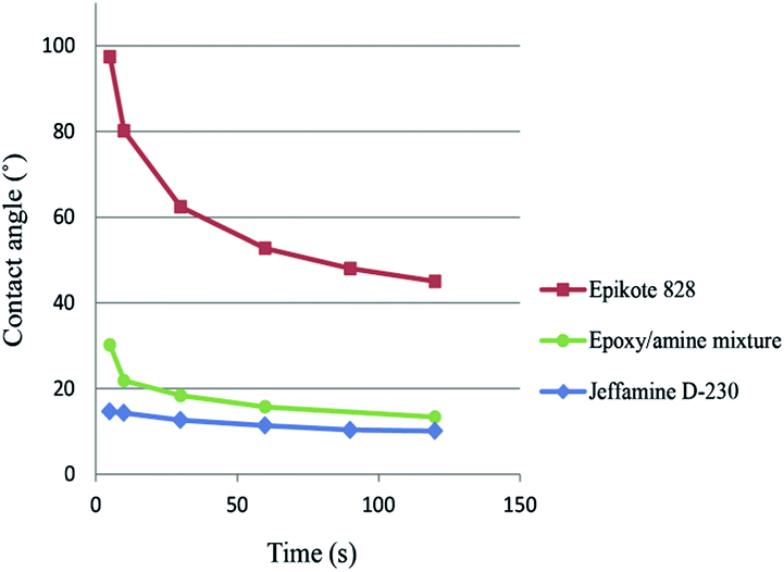 | ||
| Fig. 4 Contact angle measurements of the epoxy/amine polymer mixture and the individual components on a SWCNT film. | ||
SEM images taken of the bottom side of the peeled-off film show domains of plain polymer in areas with SWCNTs sticking out of the polymer matrix (Fig. 5). The inhomogeneity of the film surface may be a major cause of the decrease in the film resistance measured on the bottom side. However, previous experience with similar CNT–polymer composites36–38 prove that no matter what the polymer is, the CNTs are far from reaching their maximum potential (that of the pure CNTs) once they are inside a polymer matrix. This may also be due to the different natures of the interfaces and interphases formed when mixing two different components. However, measuring the resistance of the bottom side of a peeled-off film makes it virtually impossible to know the resistance of the SWCNT network alone after embedding it into the polymer.
 | ||
| Fig. 5 SEM images taken of the bottom of a peeled off SWCNT/polymer composite film (a–d) with a Au coating for emphasized contrast and (e and f) without a Au coating for emphasized aspect ratio. | ||
In situ resistance measurements during polymer impregnation
In order to have direct access to the SWCNTs after embedding them into a polymer matrix, and to be able to measure the resistance of the network during polymer impregnation, and even during the curing process, we developed a system that allowed us to perform in situ resistance measurements. For this purpose, two gold electrodes were applied via sputtering onto two opposite edges of the SWCNT film. These electrodes were connected to a multimeter to allow direct measurement of the film's resistance while the polymer was subsequently added (Fig. 6). Because the electrodes were in direct contact with the SWCNT network before polymer impregnation, and the entire film area between them was fully covered by the polymer, the resistance measured between the two electrodes was the resistance of the SWCNT network before, during and after polymer impregnation. The same system can be used to analyze the influence of the individual components of the epoxy/amine polymer mixture on the SWCNT network by applying only one component at a time and comparing the results with the overall effect of the polymer mixture.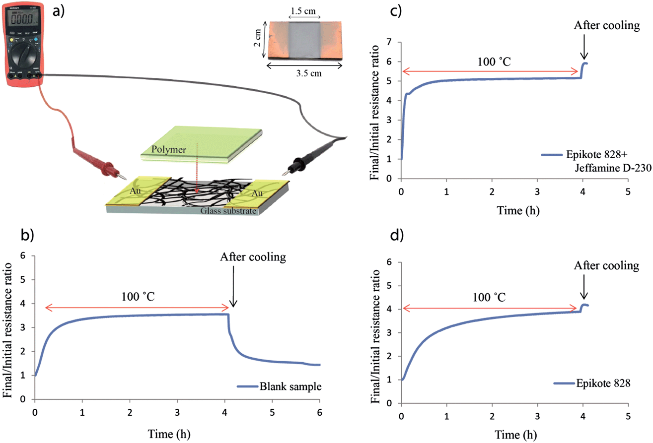 | ||
| Fig. 6 (a) Schematic of our in situ resistance measurement setup and examples of the final/initial resistance ratio curves obtained during (b) a blank measurement, (c) a polymer mixture impregnation and (d) an epoxy resin impregnation. | ||
SWCNTs are known to be highly sensitive to different gas exposures39,40 which can cause significant changes in their electronic and transport properties due to chemical doping.41 The adsorption of different gas molecules on the surface of the nanotubes can modulate the carrier concentrations by generating a surplus or a deficiency of valence electrons and implicitly modifying the CNTs' electrical behaviour. The dopant component can act as an electron donor (n-type doping) or electron acceptor (p-type doping). Studies have shown that a SWCNT film held under vacuum at room temperature can have a 15% decrease in resistance upon air exposure,42 while exposing unpurified SWCNTs to humid air after heating them up to 350 °C can lead to an up to 4 fold decrease in resistance.43 Other researchers support the hypothesis that the adsorption of gas molecules changes the value of the Schottky barrier build-up between the SWCNTs and the metal electrode.44 They support the idea that the gas molecules in the junction region can change the metal work function and the Fermi level alignment. Therefore resistance fluctuations upon heating or air exposure can be due to changes in the Schottky barriers of the metal–nanotube junctions, and not necessarily due to the doping/dedoping of the SWCNTs.
In order to avoid resistance fluctuations due to gas and water adsorption from air, after the final 400 °C thermal treatment, all of the samples were exposed to air overnight to reach saturation and a constant resistance value. Blank in situ resistance measurements were performed on a series of samples in an oven at 100 °C for 4 hours, the conditions needed for curing the polymer mixture. The results showed an average resistance increase of 3.1 fold before cooling (example in Fig. 6b), most likely due to desorption of water and gasses from the films upon heating. This value rapidly decreased as soon as the samples were taken out of the oven for cooling due to the readsorption of gasses and water at room temperature.
The same type of measurements were performed while adding only one component of the polymer mixture to separate any possible individual effects on the resistance of the SWCNT network. Measurements performed after impregnating the film with Epikote 828 alone for 4 hours at 100 °C show an average resistance increase of 3.6 fold before cooling (example in Fig. 6d), slightly higher than for the blank samples. Because Jeffamine D-230 is a volatile amine, measurements for the amine component alone were performed at room temperature, showing an average resistance increase of 4.9 fold. If we take into consideration the ratios of the blank samples, we can estimate a resistance increase of up to 15 fold after amine impregnation upon heating at 100 °C for 4 hours. Amines have been shown to have a n-type doping effect on SWCNTs45,46 and are expected to influence the resistance of the SWCNT network to a certain degree, especially if the carbon nanotubes are p-type doped by the oxygen in air42,47 or other gas molecules.
When mixing the two components together and impregnating the SWCNT film, the final/initial resistance ratio after curing the polymer for 4 hours at 100 °C was 4.3 before cooling (example in Fig. 6c). In order to obtain a 1:1 epoxy/amine ratio (based on an epoxy group/NH equivalent), the amine represents only 24.3 wt% of the epoxy/amine mixture. Therefore the resistance increase may be due not only to a cumulated effect of the two components, but also to the formation of a polymeric network during the curing process.
All of the samples coated with a polymer (epoxy resin alone or the epoxy/amine mixture) and heated at 100 °C had a resistance increase of 1.15 fold after cooling, due to the semiconductor behaviour of the SWCNTs. When the SWCNTs are covered in a polymer, they can no longer adsorb water and gasses when cooled in air.
Each SWCNT film prepared is unique and can have a slightly different thickness compared to others, so the question of whether or not the results of different experiments can be compared is important. In order to ensure the reproducibility of our experiments, we prepared SWCNT films with thicknesses varying from 10 to 140 nm. Thickness measurements involve damaging the samples to measure the height profiles across scratches in the film, therefore SWCNT films were prepared on large glass substrates which were subsequently cut into 2 cm × 3.5 cm samples. Half of these were used for correlating the thickness with resistance and transmittance measurements, while the other half were used for polymer impregnation. The absorbance as a function of thickness curve shows a pseudo-linear dependency within the 10–140 nm thickness range (Fig. 7a). This curve, along with the resistance vs. thickness (Fig. 7b) curve, can be used to approximate the thicknesses of the SWCNT films used for polymer impregnation.
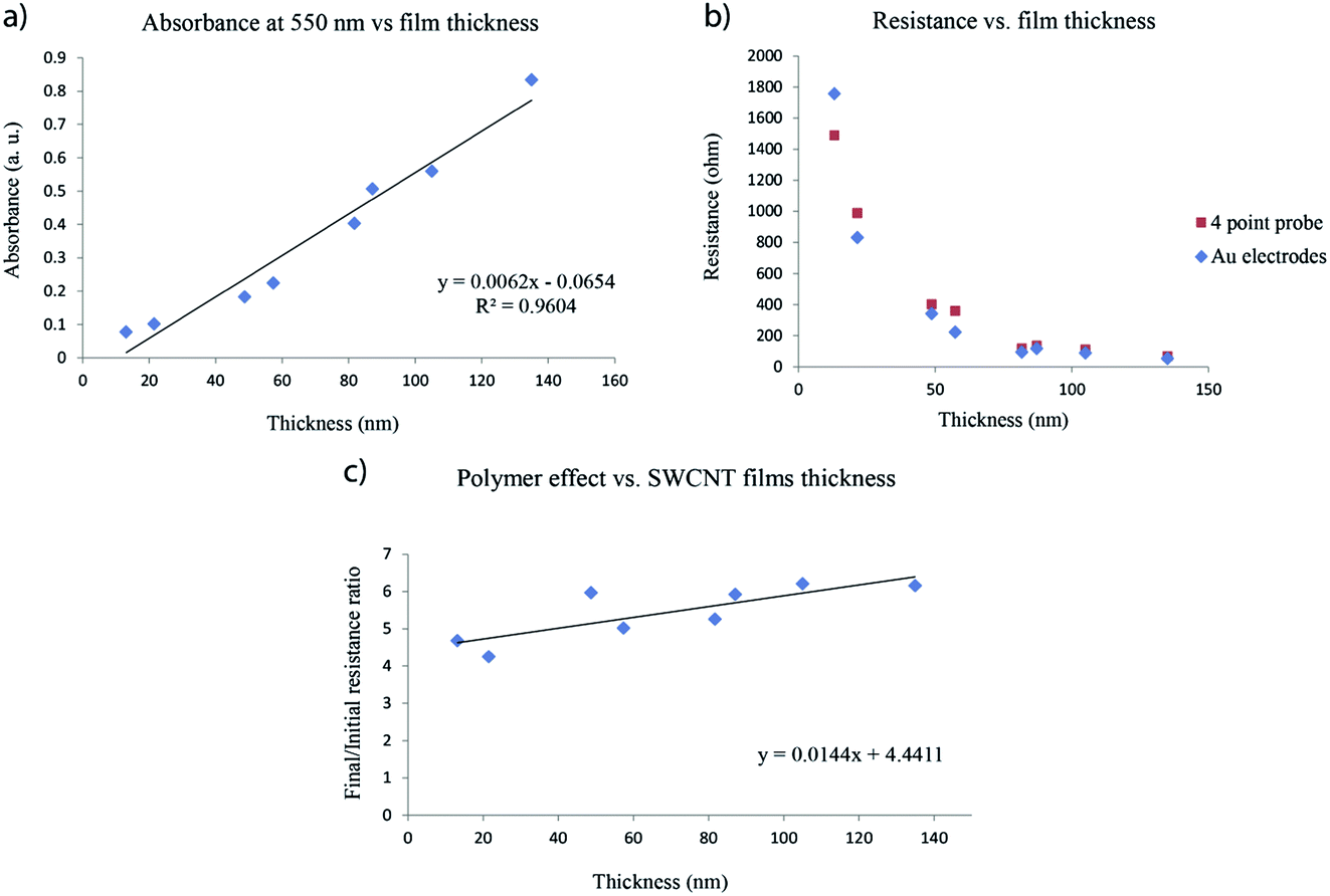 | ||
| Fig. 7 (a) Absorbance, (b) resistance and (c) polymer impregnation effect depending on the SWCNT film thickness. | ||
In situ resistance measurements performed on films of different thicknesses after impregnating with the epoxy/amine mixture and curing the polymer for 4 hours at 100 °C, show that there is no major difference in the final/initial resistance ratios between 10 nm films and 140 nm films (Fig. 7c). The average final/initial resistance ratios (after cooling) increase from 5 to 6 within this thickness range. This means that experiments performed on SWCNT films of 20–40 nm thickness are comparable despite minor thickness variations. These results are similar to those of Noh et al.48 who impregnated 12 μm thick multi-walled carbon nanotube (MWCNT) mats with cyclic butylene terephthalate (CBT), by compressing them with a heating press. The resistance of the MWCNT mats increased 2 to 9 fold (depending on the compression pressure) after polymer addition.
Conclusions
We have adapted and improved a preparation technique for SWCNT thin films which represent our reference networks with good electrical properties. These films were used to study the polymer matrix effect on an already existing SWCNT network during polymer impregnation. We developed an in situ resistance measurement technique that allowed us to have direct access to the conductive network during polymer impregnation, and also during the curing process of the polymer matrix. These measurements showed that polymer impregnation is not the only factor that can influence the behaviour of the carbon nanotubes; they showed that different components of a polymer mixture can have different effects on the electrical properties of a SWCNT network aside from the formation of a polymeric network during the curing process. Blank measurements showed that air and temperature exposure can also affect the electrical behaviour of the carbon nanotubes, even without the addition of a polymer component. These results prove that in order to prepare an efficient composite material, it is important first to understand the effects that any factor introduced in the preparation process can have on each of the components. Further studies will be performed in order to understand how the polymer impregnation process and the newly formed interfaces affect the electrical contacts between the carbon nanotubes. These studies will contribute to the improvement of future polymer composites efficiencies.Acknowledgements
This research forms part of the research programme of the Dutch Polymer Institute (DPI), project #756 (CoCoCo). The authors would also like to thank Dr J. G. P. Goossens (TU/e) for his support.References
- W. Marx and A. Barth, Phys. Status Solidi B, 2008, 245, 2347–2351 CrossRef CAS.
- J. N. Coleman, U. Khan, W. J. Blau and Y. K. Gun'ko, Carbon, 2006, 44, 1624–1652 CrossRef CAS PubMed.
- J. Bernholc, D. Brenner, M. B. Nardelli, V. Meunier and C. Roland, Annu. Rev. Mater. Res., 2002, 32, 347–375 CrossRef CAS.
- J. Hone, M. C. Llaguno, M. J. Biercuk, A. T. Johnson, B. Batlogg, Z. Benes and J. E. Fischer, Appl. Phys. A: Mater. Sci. Process., 2002, 74, 339–343 CrossRef CAS.
- M. S. Dresselhaus, G. Dresselhaus, J. C. Charlier and E. Hernandez, Philos. Trans. R. Soc., A, 2004, 362, 2065–2098 CrossRef CAS PubMed.
- H. Kataura, Y. Kumazawa, Y. Maniwa, I. Umezu, S. Suzuki, Y. Ohtsuka and Y. Achiba, Synth. Met., 1999, 103, 2555–2558 CrossRef CAS.
- Z. C. Wu, Z. H. Chen, X. Du, J. M. Logan, J. Sippel, M. Nikolou, K. Kamaras, J. R. Reynolds, D. B. Tanner, A. F. Hebard and A. G. Rinzler, Science, 2004, 305, 1273–1276 CrossRef CAS PubMed.
- F. Mirri, A. W. K. Ma, T. T. Hsu, N. Behabtu, S. L. Eichmann, C. C. Young, D. E. Tsentalovich and M. Pasquali, ACS Nano, 2012, 6, 9737–9744 CrossRef CAS PubMed.
- D. S. Hecht, A. M. Heintz, R. Lee, L. B. Hu, B. Moore, C. Cucksey and S. Risser, Nanotechnology, 2011, 22, 075201 CrossRef PubMed.
- M. B. Bryning, M. F. Islam, J. M. Kikkawa and A. G. Yodh, Adv. Mater., 2005, 17, 1186–1191 CrossRef CAS.
- Y. Zhao, H. P. Hong and J. S. Welsh, Proc. SPIE7404, Nanostructured Thin Films II, 2009, 74040H Search PubMed.
- M. J. Biercuk, M. C. Llaguno, M. Radosavljevic, J. K. Hyun, A. T. Johnson and J. E. Fischer, Appl. Phys. Lett., 2002, 80, 2767–2769 CrossRef CAS PubMed.
- K. D. Ausman, R. Piner, O. Lourie, R. S. Ruoff and M. Korobov, J. Phys. Chem. B, 2000, 104, 8911–8915 CrossRef CAS.
- Y. Y. Huang and E. M. Terentjev, Polymers, 2012, 4, 275–295 CrossRef PubMed.
- N. Minami, Y. J. Kim, K. Miyashita, S. Kazaoui and B. Nalini, Appl. Phys. Lett., 2006, 88, 093123 CrossRef PubMed.
- T. Takahashi, K. Tsunoda, H. Yajima and T. Ishii, Jpn. J. Appl. Phys., Part 1, 2004, 43, 3636–3639 CrossRef CAS.
- U. Dettlaff-Weglikowska, J. M. Benoit, P. W. Chiu, R. Graupner, S. Lebedkin and S. Roth, Curr. Appl. Phys., 2002, 2, 497–501 CrossRef.
- Y. Zhao, B. Mannhalter, H. P. Hong and J. S. Welsh, J. Nanosci. Nanotechnol., 2010, 10, 5776–5782 CrossRef CAS PubMed.
- D. M. Bigg, Polym. Eng. Sci., 1979, 19, 1188–1192 CAS.
- G. H. Zheng, J. S. Wu, W. P. Wang and C. Y. Pan, Carbon, 2004, 42, 2839–2847 CrossRef CAS PubMed.
- J. Z. Kovacs, B. S. Velagala, K. Schulte and W. Bauhofer, Compos. Sci. Technol., 2007, 67, 922–928 CrossRef CAS PubMed.
- C. A. Martin, J. K. W. Sandler, M. S. P. Shaffer, M. K. Schwarz, W. Bauhofer, K. Schulte and A. H. Windle, Compos. Sci. Technol., 2004, 64, 2309–2316 CrossRef CAS PubMed.
- J. K. W. Sandler, J. E. Kirk, I. A. Kinloch, M. S. P. Shaffer and A. H. Windle, Polymer, 2003, 44, 5893–5899 CrossRef CAS.
- X. K. Li, F. Gittleson, M. Carmo, R. C. Sekol and A. D. Taylor, ACS Nano, 2012, 6, 1347–1356 CrossRef CAS PubMed.
- F. M. Smits, Bell Syst. Tech. J., 1958, 37, 711–718 CrossRef.
- M. J. O'Connell, P. Boul, L. M. Ericson, C. Huffman, Y. H. Wang, E. Haroz, C. Kuper, J. Tour, K. D. Ausman and R. E. Smalley, Chem. Phys. Lett., 2001, 342, 265–271 CrossRef.
- W. Gomulya, G. D. Costanzo, E. J. F. de Carvalho, S. Z. Bisri, V. Derenskyi, M. Fritsch, N. Frohlich, S. Allard, P. Gordiichuk, A. Herrmann, S. J. Marrink, M. C. dos Santos, U. Scherf and M. A. Loi, Adv. Mater., 2013, 25, 2948–2956 CrossRef CAS PubMed.
- W. Choi, S. Ohtani, K. Oyaizu, H. Nishide and K. E. Geckeler, Adv. Mater., 2011, 23, 4440–4443 CrossRef CAS PubMed.
- W. Zhou, J. Vavro, N. M. Nemes, J. E. Fischer, F. Borondics, K. Kamaras and D. B. Tanner, Phys. Rev. B: Condens. Matter Mater. Phys., 2005, 71, 205423 CrossRef.
- R. Saito, M. Hofmann, G. Dresselhaus, A. Jorio and M. S. Dresselhaus, Adv. Phys., 2011, 60, 413–550 CrossRef CAS.
- S. Costa, E. Borowiak-Palen, M. Kruszynska, A. Bachmatiuk and R. J. Kalenczuk, Mater. Sci.-Pol., 2008, 26, 433–441 CAS.
- A. Jorio, M. A. Pimenta, A. G. Souza, R. Saito, G. Dresselhaus and M. S. Dresselhaus, New J. Phys., 2003, 5, 139 CrossRef.
- Y. Miyata, K. Mizuno and H. Kataura, J. Nanomater., 2011, 786763 Search PubMed.
- R. Schonfelder, F. Aviles, A. Bachmatiuk, J. V. Cauich-Rodriguez, M. Knupfer, B. Buchner and M. H. Rummeli, Appl. Phys. A: Mater. Sci. Process., 2012, 106, 843–852 CrossRef.
- N. N. A. H. Meis, L. G. J. van der Ven, R. A. T. M. van Benthem and G. de With, Prog. Org. Coat., 2014, 77, 176–183 CrossRef CAS PubMed.
- J. Sandler, M. S. P. Shaffer, T. Prasse, W. Bauhofer, K. Schulte and A. H. Windle, Polymer, 1999, 40, 5967–5971 CrossRef CAS.
- A. Allaoui, S. Bai, H. M. Cheng and J. B. Bai, Compos. Sci. Technol., 2002, 62, 1993–1998 CrossRef CAS.
- N. Grossiord, P. J. J. Kivit, J. Loos, J. Meuldijk, A. V. Kyrylyuk, P. van der Schoot and C. E. Koning, Polymer, 2008, 49, 2866–2872 CrossRef CAS PubMed.
- J. J. Zhao, A. Buldum, J. Han and J. P. Lu, Nanotechnology, 2002, 13, 195–200 CrossRef CAS.
- Y. Wang and J. T. W. Yeow, J. Sens., 2009, 2009, 24 Search PubMed.
- J. E. Fischer, Acc. Chem. Res., 2002, 35, 1079–1086 CrossRef CAS PubMed.
- P. G. Collins, K. Bradley, M. Ishigami and A. Zettl, Science, 2000, 287, 1801–1804 CrossRef CAS.
- Y. Maniwa, Y. Kumazawa, Y. Saito, H. Tou, H. Kataura, H. Ishii, S. Suzuki, Y. Achiba, A. Fujiwara and H. Suematsu, Mol. Cryst. Liq. Cryst., 2000, 340, 671–676 CrossRef CAS.
- P. Bondavalli, P. Legagneux and D. Pribat, Sens. Actuators, B, 2009, 140, 304–318 CrossRef CAS PubMed.
- R. B. Koizhaiganova, D. H. Hwang, C. J. Lee, S. Roth and U. Dettlaff-Weglikowska, Phys. Status Solidi B, 2010, 247, 2793–2796 CrossRef CAS.
- D. R. Samarajeewa, G. R. Dieckmann, S. O. Nielsen and I. H. Musselman, Carbon, 2013, 57, 88–98 CrossRef CAS PubMed.
- A. Tchernatinsky, S. Desai, G. U. Sumanasekera, C. S. Jayanthi, S. Y. Wu, B. Nagabhirava and B. Alphenaar, J. Appl. Phys., 2006, 99, 034306 CrossRef PubMed.
- Y. J. Noh, H. S. Kim and S. Y. Kim, Carbon Letters, 2012, 13, 243–247 CrossRef.
| This journal is © The Royal Society of Chemistry 2014 |