 Open Access Article
 This Open Access Article is licensed under a Creative Commons Attribution-Non Commercial 3.0 Unported Licence
Towards low-cost, environmentally friendly printed chalcopyrite and kesterite solar cells
Hamed
Azimi
*a,
Yi
Hou
ac and
Christoph J.
Brabec
ab
aInstitute of Materials for Electronics and Energy Technology (I-MEET), Department of Materials Science and Engineering, Friedrich-Alexander University Erlangen-Nuremberg, Martensstrasse 7, 91058 Erlangen, Germany. E-mail: hamed.azimi@fau.de
bBavarian Center for Applied Energy Research (ZAE Bayern), Haberstr. 2a, 91058 Erlangen, Germany
cErlangen Graduate School in Advanced Optical Technologies (SAOT), Paul-Gordan-Str. 6, 91052 Erlangen, Germany
First published on 5th March 2014
Abstract
Solution-processed organic and inorganic semiconductors offer a promising path towards low-cost mass production of solar cells. Among the various material systems, solution processing of multicomponent inorganic semiconductors offers considerable promise due to their excellent electronic properties and superior photo- and thermal stability. This review surveys the recent developments of “all solution-processed” copper–indium (–gallium)-chalcogenide (CuInS2, CuInSe2 and Cu(In, Ga)(Se, S)2) chalcopyrites and copper–zinc–tin-chalcogenide (Cu2ZnSnS4 and Cu2ZnSnSe4 (CZTS(e))) kesterite solar cells. A brief overview further addresses some of the most critical material aspects and associated loss mechanisms in chalcopyrite and kesterite devices. Today's state-of-the-art performance as well as future challenges to achieve low-cost and environmentally friendly production is discussed.
 Hamed Azimi | Hamed Azimi received his MEng in Electrical Engineering from Ferdowsi University of Mashhad, Iran. In December 2006, he joined Konarka Austria to study for a PhD under the supervision of Prof. Christoph. J. Brabec (Konarka) and Prof. Kurt Hingerl (Johannes Kepler University Linz, Austria). He obtained his PhD in Engineering Sciences in 2011. Since 2011, he has been a postdoctoral fellow in the group of Prof. Brabec in the institute of Materials for Electronics and Energy Technology (i-MEET) at the Friedrich Alexander University Erlangen-Nürnberg, where he leads the group of solution processed inorganic and hybrid semiconductors for photovoltaic application. |
 Yi Hou | Yi Hou is currently a PhD student under the supervision of Prof. Christoph J. Brabec at the institute of Materials for Electronics and Energy Technology (i-MEET) at Friedrich Alexander University Erlangen- Nürnberg (FAU). He received his MEng degree in Materials Science and Engineering from Beijing University of Chemical Technology (2012). He was awarded the Erlangen Graduate School in Advanced Optical Technologies (SAOT) award in 2013. His research interest includes low-temperature solution processed inorganic and hybrid semiconductors and their applications in photovoltaics. |
 Christoph J. Brabec | Christoph J. Brabec is holding the chair “Materials for Electronics and Energy Technology (i-MEET)” at the materials science department of the Friedrich Alexander University Erlangen-Nürnberg. Further, he is the scientific director of the Erlangen division of the Bavarian Research Institute for Renewable Energy (ZAE Bayern, Erlangen), board member of the ZAE Bavaria and board member of the Energy Campus Nurnberg. Before joining the university, he was in SIEMENS research labs as the project leader for organic semiconductor devices and in Konarka Technologies Inc. as CTO. He is author and co-author of more than 200 papers and nearly 100 patents and patent applications. |
Broader contextPhotovoltaics as the only truly portable renewable-energy conversion technology available today demonstrate strong commercial growth and hold promise for significant market opportunities. Among various solar cell technologies, thin-film technologies are one of the cost-competitive solar technologies due to reduced material and fabrication costs. However, the production of thin film solar cells typically relies on capex intense vacuum-based techniques, and/or high-temperature processes, both increasing manufacturing costs. Solution processing of multicomponent inorganic solar cells is considered as a promising alternative fabrication route to the conventional high cost vacuum techniques. |
1. Introduction
Thin film solar cell technology has a major potential for further cost reductions, provided that the expected increases in production facility size and efficiency are realized.1–3Fig. 1 compares the world record single cell efficiencies of various types of thin film solar cell technologies including organic, inorganic and hybrid semiconducting materials. Among the various types of thin-film solar cells, Cu(In, Ga)(Se, S)2 (CIGSSe) is today the combination that delivers one of the highest power conversion efficiencies. The CIGSSe world record efficiency above 20% was only recently demonstrated,4,5 and highlighted how close CIGSSe already is to poly-Si technology. Although CIGSSe technology has a number of attractive features, the deposition of the absorber layer is a complex process requiring vacuum technologies. The common approach for the production of copper indium gallium diselenide (CIGSe) solar cells is currently based on the co-evaporation of individual metallic elements or on sputtering of the suitable metal precursors followed by a crystallization step at high temperature in the presence of Se vapor and/or hydrogen selenide gas (known as depositon-reaction or a sequential process). These processes are generally challenging due to the difficulty to control the film composition over a large area and the use of toxic gases for selenization. Over the past few years, the quest for low cost production focused more and more towards the non-vacuum deposition methods. The non-vacuum approaches for deposition of multicomponent inorganic absorber layers can be generally summarized under three main categories: (i) solution deposition based on electrochemical and chemical bath-based techniques like electrodeposition, electroplating and chemical bath deposition (CBD). (ii) Printing/coating from molecular-based precursor solutions. (iii) Printing/coating from particulate-based solutions. Electrodeposition is one of the well-established electrochemical techniques in the electronics industry.6 However in this method, the deposition of multicomponent semiconductors like CIGSe is generally a complex process as the different elements have different redox potentials and reduction kinetics.7,8 Multistep deposition might be necessary to provide a good control of stoichiometry and phase homogeneity. Among the approaches mentioned, the particulate- and precursor-based approaches have recently received a great deal of attention due to their potential to simplify the fabrication processing for large-scale manufacturing. | ||
| Fig. 1 Comparison between the world record efficiencies reported for various thin film solar cell technologies including for single cell and submodule devices. (Data extracted from the solar cell efficiency table reported by Green et al.9) Note: thin film GaAs and polycrystalline solar cells are not included in this comparison. | ||
In this article, our main focus is dedicated to the solution-processed fabrication of chalcopyrite CuInS2 (CIS), CuInSe2 (CISe) and Cu(In, Ga)(Se, S)2 (CIGSSe) solar cells, addressing all the various methods like molecular, and particulate-based solutions as well as their hybrid combinations. Furthermore, as an important alternative to the CIGSSe technology, we also review the current state-of-the-art fabrication routes for solution processed kesterite Cu2ZnSnS4 (CZTS), Cu2ZnSnSe4 (CZTSe), and Cu2ZnSn(S,Se)4 (CZTSSe) solar cells.
2. Fundamental aspects of chalcopyrite and kesterite solar cells
2.1. Device concept
Fig. 2 shows a classical configuration of CIGSe and CZTSe solar cells, which is based on a heterojunction cell structure. The absorber layer with a thickness of typically 1–2 μm is deposited on molybdenum-coated soda-lime glass substrates. The heterojunction is then formed by the deposition of an n-type buffer layer (usually 50 nm CdS layer deposited by chemical bath deposition), the sputtering deposition of an intrinsic i-ZnO (typically with a thickness of 40–70 nm) and eventually of a transparent conductive oxide layer as the window layer (normally a heavily doped ZnO![[thin space (1/6-em)]](https://www.rsc.org/images/entities/char_2009.gif) :Al or an indium-doped tin oxide (ITO) layer). A schematic band diagram of a CIGSe solar cell under zero-bias voltage condition is shown in Fig. 2. Some of the most critical recombination paths governing the diode current of such a solar cell structure are: recombination at the absorber surface, in the absorber bulk, at the absorber back contact, and in the absorber space charge region (SCR). The high probability for the charge carrier recombination at the absorber surface is one of the main disadvantages of such a cell structure; the advantage however is a negligible recombination in the buffer and window layer due to the large bandgap recombination in those regions. The high recombination at the heterojunction can be circumvented to a large extent by the proper design of the band diagram.10 The highly doped CdS layer with a large bandgap of 2.4 eV is being typically used as an n-type layer in junction with a p-type CIGS or CZTS absorber layer in order to reduce the collection losses due to surface recombination (SR) of carriers photogenerated by short wavelength light and to transport electrons from the junction to the front surface. The recombination in the quasi-neutral region (QNR) largely depends on the bandgap gradients. The opportune bandgap gradient in chalcopyrite and kesterite solar cells can be achieved by controlled incorporation of Ga or S. Some examples of bandgap grading for solution processed chalcopyrite and kesterite solar cells are given in the following sections. The poor collection of carriers photogenerated at the back contact can be improved by enhancing the electron diffusion length (Ln). A longer Ln can be achieved by passivating the interfaces, or increasing the crystallite size.11
:Al or an indium-doped tin oxide (ITO) layer). A schematic band diagram of a CIGSe solar cell under zero-bias voltage condition is shown in Fig. 2. Some of the most critical recombination paths governing the diode current of such a solar cell structure are: recombination at the absorber surface, in the absorber bulk, at the absorber back contact, and in the absorber space charge region (SCR). The high probability for the charge carrier recombination at the absorber surface is one of the main disadvantages of such a cell structure; the advantage however is a negligible recombination in the buffer and window layer due to the large bandgap recombination in those regions. The high recombination at the heterojunction can be circumvented to a large extent by the proper design of the band diagram.10 The highly doped CdS layer with a large bandgap of 2.4 eV is being typically used as an n-type layer in junction with a p-type CIGS or CZTS absorber layer in order to reduce the collection losses due to surface recombination (SR) of carriers photogenerated by short wavelength light and to transport electrons from the junction to the front surface. The recombination in the quasi-neutral region (QNR) largely depends on the bandgap gradients. The opportune bandgap gradient in chalcopyrite and kesterite solar cells can be achieved by controlled incorporation of Ga or S. Some examples of bandgap grading for solution processed chalcopyrite and kesterite solar cells are given in the following sections. The poor collection of carriers photogenerated at the back contact can be improved by enhancing the electron diffusion length (Ln). A longer Ln can be achieved by passivating the interfaces, or increasing the crystallite size.11
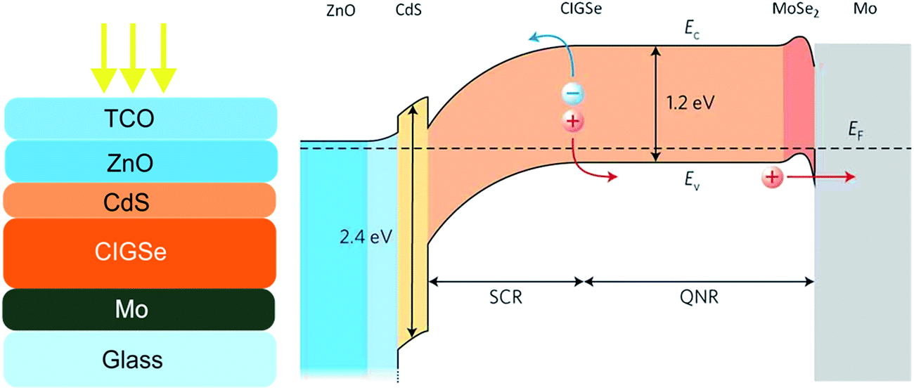 | ||
| Fig. 2 Left – a schematic layer structure of a classical CIGSe solar cell. Right – a schematic band profile of a typical CIGSe solar cell under zero-bias voltage condition. The image of the band profile is reprinted with permission from ref. 12, Copyright 2011, Nature Publishing Group. | ||
2.2. Grain boundaries and defects
In polycrystalline solar cells, the size of grains and the recombination velocity at the grain boundaries (GBs) are the key parameters to determine the rate of the charge carrier recombination. One primary influence of the GBs is the interruption of the long-range order in the crystal. A simple relationship between the effective diffusion length (Leff) for a polycrystalline material and a monocrystalline material can be defined as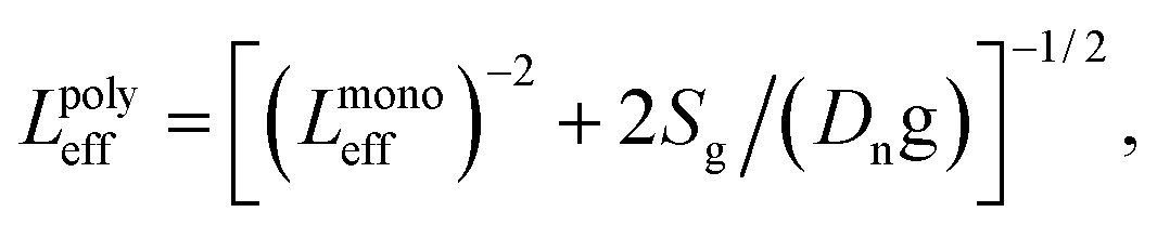 | (1) |
With respect to the different loss mechanisms discussed, it is important to understand the formation of the various defects and secondary phases in chalcopyrites and kesterites. Defects may appear as single defect states with well defined energy levels within the bandgap or as multiple defect states and defect distributions with a quasi continuous state density in the bandgap.10 In CIGSSe, the first-principle investigation showed that the indium-on-copper-antisites (InCu) and the copper vacancy (VCu) are, respectively, the dominant donor and acceptor defects.21,22 The acceptor defect VCu is found to have a shallow ionization energy level and lower formation energy than the donor defects as InCu (GaCu) and Cui, explaining therefore the intrinsic p-type conductivity and also the difficulty in the control of n-type doping in this material. Furthermore in ternary chalcopyrites, due to the energetically favorable donor–acceptor compensation between VCu and InCu, there is a high probability of formation of defect clusters like [2VCu + InCu] and even the ordered defect compound such as CuIn5Se8.23 In CZTS, VCu has similarly a low formation energy and becomes dominant in the case of Cu-poor and Zn-rich samples. Moreover, the cause of frequently observed non-stoichiometric kesterite samples can be explained on grounds of a strong tendency towards formation of self-compensated defect clusters, like [VCu + ZnCu], [ZnSn + 2ZnCu] and [2CuZn + SnZn]23,24 (see Table 1 for a comparison between the dominant defects in chalcopyrites and kesterites).
| CuInSe2 | CuGaSe2 | Cu2ZnSnSe4 | Cu2ZnSnS4 | |
|---|---|---|---|---|
| Bandgap (eV) | 1.04 | 1.68 | 1.0 | 1.5 |
| Intrinsic conductivity | p-type | p-type | p-type | p-type |
| Hole-generating acceptors | V Cu − | V Cu − | CuZn−, VCu− | CuZn−, VCu− |
| High-population deep donors | GaCu2+ | SnZn2+, VS2+ | ||
| High-population clusters | 2VCu + InCu | 2VCu + GaCu | V Cu + ZnCu | V Cu + ZnCu |
| CuZn + ZnCu | CuZn + ZnCu | |||
| 2CuZn + SnZn | 2CuZn + SnZn | |||
| ZnSn + 2ZnCu | ZnSn + 2ZnCu | |||
| Electron trapping clusters | 2VCu + GaCu | 2CuZn + SnZn |
For solution processed solar cells, the effects of grain boundaries and the defects can be very different from the devices fabricated based on the conventional vacuum deposition routes. The defect chemistry and the mechanisms of phase transformation can vary markedly depending on the initial solution precursors and the temperature used for the film deposition and the phase transformation. The losses induced by the smaller size of grains and the possible impurities from the precursors may exert a profound impact on the final device performance. To date, there have been very limited studies to provide in-depth insights into the properties and the loss mechanisms of solution processed chalcopyrite and kesterite devices. Fundamental insights using advanced characterization methods are still necessary to overcome the limitations in these devices.
2.3. Characterizations
Raman spectroscopy, X-ray diffraction, energy-/wavelength dispersive X-ray spectroscopy and X-ray fluorescence are commonly being used to obtain information on crystalline quality, phase purity and chemical composition. Among the techniques mentioned above, Raman spectroscopy is an extremely useful technique that provides insight into the lattice strains and the existence and spatial distribution of different phases. Furthermore, in the preparation of molecular precursor solutions, Raman measurements can be used to analyze the degree of intermixing between the precursor components.25 In CISSe samples, Raman spectroscopy can be used to distinguish the desired stable chalcopyrite (CH) from the metastable copper–gold CuAu (CA) and the metastable copper rich CuIn5(S, Se)8 structure.26–29 For CZTS samples, while the coexistence of CZTS, Cu2SnS3 (CTS), and ZnS may not be distinguishable by diffraction techniques, Raman analysis is able to detect and distinguish between these phases through their characteristic scattering peaks.30–33 The employment of Raman spectroscopy at resonance conditions is shown to be essential for the distinction between the secondary phases in kesterites.34 For a detailed overview on assignment of Raman peaks to different binary and ternary secondary phases related to the CZTS system, see ref. 30 and 34. To monitor the phase formation/transition during the thermal annealing, in situ techniques and thermal analyses like thermogravimetric analysis and differential thermal analysis are being implemented.35–38To obtain information about the defect physics and their relationship to the device performance, characterization tools such as photoluminescence (PL),39–41 admittance spectroscopy, deep level transient spectroscopy (DLTS)42–44 and Hall measurements45,46 are relevant. A combination of these techniques is generally necessary to analyze the shallow, mid-bandgap as well as the deep defects; while admittance measurements generally provide information on the deep defects, information on the density and the energy of shallow defects can be obtained by Hall and PL measurements.15 In PL, studying the excitation intensity and the temperature dependence of the emission peaks sheds light onto the activation energies of the defects as well as the nature of the associated transitions.22,46 At low temperatures and low excitation intensities, the PL spectrum can be dominated by the band–tail (BT) recombination. The BT recombination is the emission band that follows the band edge potential fluctuations originating from the local deviations in the distribution of donor and acceptor states (see Fig. 3). For instance, comparing the defect properties of Cu-poor chalcopyrite and kesterite samples, a recent study found the higher probability of nonradiative recombination for the latter system. This conclusion was drawn on the basis of two observations: (1) the lower PL intensity and (2) the significantly high excitation densities needed for transition from a band-tail (BT) to a band-to-band (BB) recombination in CZTS. This result is consistent with the fact that kesterite has greater tendency towards formation of point defects with associated electronic states near the midgap.22
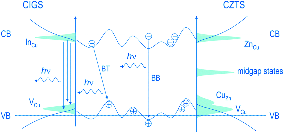 | ||
| Fig. 3 Schematics of the band diagram for Cu-poor CIGSe and Cu-poor, Zn-rich CZTS, which represent the dominance of the band-tail (BT) and band-to-band (BB) transitions between delocalized donor and acceptor states. The energetic bands show potential fluctuations due to the local deviations in the distribution of donor and acceptor states. Reprinted with permission from ref. 22, Copyright 2011, American Physical Society. | ||
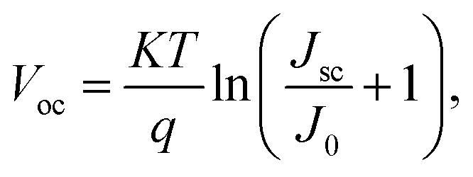
Another important method associated with PL spectroscopy is the time-resolved photoluminescence (TR-PL). TR-PL is used to directly measure the minority carrier lifetime in CIGSSe and CZTSSe devices.47,48 The low minority carrier lifetime can result in higher dark current (J0) and can therefore promote the Voc deficit in solar cell devices (eqn (2)).
 | (2) |
Fig. 4 shows a TR-PL data of a 15.2% efficient hydrazine-based CIGSSe solar cell.49 A lifetime of τ = 5.4 ± 0.2 ns was measured for this cell which is found to be lower than the lifetimes measured for high-performance vacuum-processed CIGSe solar cells (>10 ns).48
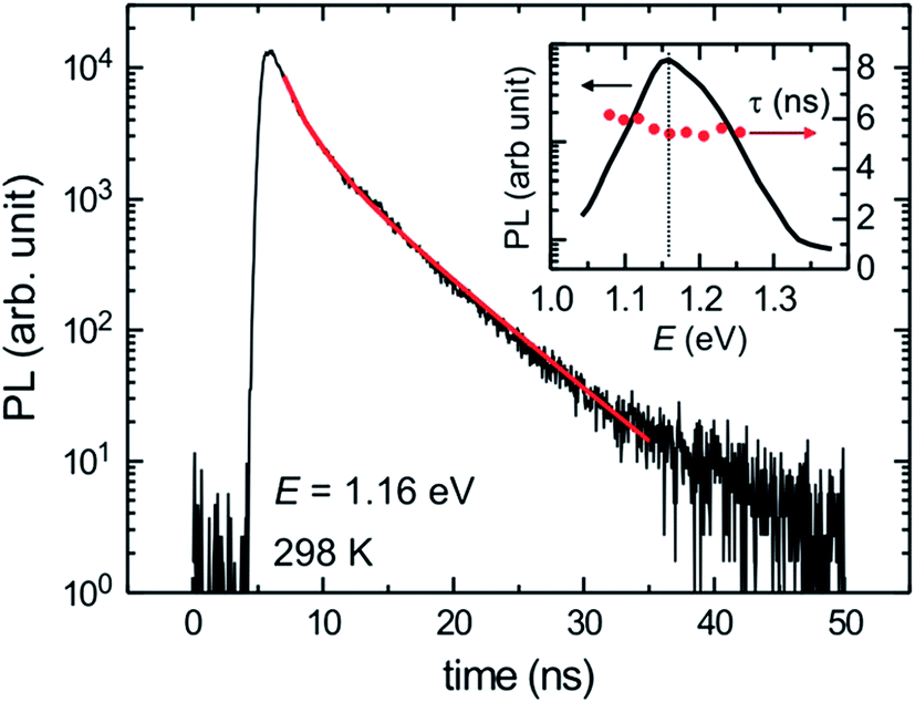 | ||
| Fig. 4 Time-resolved photoluminescence (TR-PL) trace measured for the hydrazine-processed CIGSSe with a PCE of 15.2%. Inset: the PL spectrum and the extracted lifetime in the vicinity of the band edge emission. Reprinted with permission from ref. 49, Copyright 2013, John Wiley & Sons, Ltd. | ||
To investigate the influence of GBs and their passivation on the performance of chalcopyrite and kesterite-based solar cells, scanning probe microscopy methods like scanning Kelvin probe microscopy (SKPM) and conductive probe atomic force microscopy (CP-AFM) are frequently used.50,51 The simultaneous measurement of the surface film topography along with probing the variations of electrostatic surface potential (SKPM) and the current flow/surface conductivity (CP-AFM) at GBs documents important information with relevance to solar cell operation. High-resolution mapping can help in understanding whether the device performance is limited by grain bulk, grain surface, and/or GBs. A recent study,50 comparing the surface potential maps of CIGSe, CZTS, and CZTSSe, showed similarly for all the samples higher positive surface potentials at the GBs compared to the surface of the grains. This observation suggests that in kesterites like CIGSe, GBs assist in the collection of minority carriers into the GBs. CP-AFM measurements were further used to demonstrate that there is no significant minority carrier recombination at GBs and the process of minority carrier collection by the GBs indeed occurs.
Besides the methods discussed above, a wide variety of other microscopic and spectroscopic techniques are available to study the electrical, optical, structural as well as the device properties of thin film solar cells (for a detailed overview, see ref. 52 and 53).
3. Solution processed chalcopyrite solar cells
3.1. Deposition from molecular-based precursor solution
A solution based on a mixture of different molecular precursors can be directly used to produce films with a desired stoichiometric ratio of elements, high crystallinity and good uniformity in composition.54 Chemical modifiers and sacrificial ligands are generally required to control the reaction kinetics and the solubility of precursor materials. Thermal treatment is being performed to convert the precursors into the desired phase and to remove the residual organic species. The concentration and the viscosity of the precursor solution are crucial factors impacting film formation and drying kinetics. Furthermore, the quality of the final metal chalcogenide film can be strongly influenced by the bulkiness and volatility of the sacrificial ligands. Small ligands are being preferred to avoid the formation of cracks and disruption of films during thermal decomposition.55 Heat treatment at high temperatures in a sulphur or selenium atmosphere typically is necessary in order to complete the phase transformation and to minimize the porosity of the film.56Despite the obvious superior performance of hydrazine-processed devices, the application of this process is limited by the toxicity and high reactivity of hydrazine. Recently, Zhou et al.63 reported the use of non-hydrazine solutions for processing of CuIn(S,Se)2 (CISSe) solar cells from hydrazinium precursors. The hydrazinium precursors were prepared by dissolving copper sulfide (Cu2S) and indium selenide (In2Se3) precursors in hydrazine. The Cu–In hydrazinium precursors were found to be fairly soluble in a mixture of ethanolamine (EA) and dimethyl sulfoxide (DMSO). The solubility in the EA/DMSO mixture is described by the reducing capability of EA and the tendency of the S atom in DMSO to coordinate with metal cores. The scheme in Fig. 5 illustrates the dissolution process for Cu–In hydrazinium into a solvent combination of EA/DMSO, where excessive S/Se is being added to accelerate the dissolution of precursors. The performance of solar cells fabricated by this approach was limited by the device thickness due to the lower degree of crystallinity and smaller grain size of films compared to the films from a pure hydrazine-based approach. Optimized CISSe solar cells fabricated using this method showed a device efficiency of 3.8% for an absorber film thickness of 300 nm, which is comparable to the hydrazine-based CISSe solar cells with a similar film thickness. Despite the apparent attractiveness, this technique still has the disadvantage of using hydrazine for preparation of initial precursors, which limits the applicability of the process.
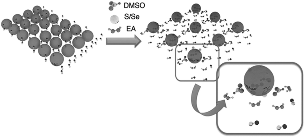 | ||
| Fig. 5 Schematic representation of the dissolution mechanism for Cu–In hydrazinium in a solvent mixture of EA and DMSO. Reprinted with permission from ref. 63, Copyright 2012, Wiley VCH. | ||
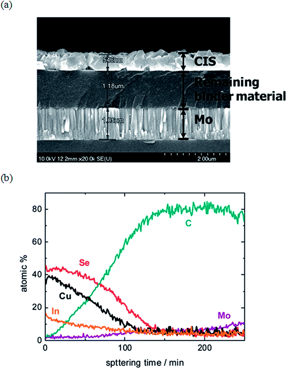 | ||
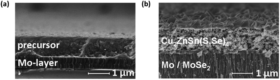
| Fig. 6 (a) Cross-sectional SEM micrographs of a selenized film prepared based on a precursor solution comprised of metal-nitrates and metal-halides in methanol. (b) The corresponding Auger electron spectroscopy (AES) data depth profile of the selenized sample, confirming the presence of an amorphous carbon layer near the back Mo electrode. Reprinted with permission from ref. 54, Copyright 2010 American Chemical Society. | ||
Based on an alcoholic solution, acetate salts of the metals, namely, copper(II) acetate and indium(III) acetate, were also used to fabricate CIGSe solar cells.68,69 For incorporation of gallium, the chloride or acetylacetonate (acac) salts of gallium were used. It was shown that a sufficiently high partial pressure of Se improves the grain size and the overall degree of crystallinity during the selenization process. Fig. 7 compares the SEM images of CIGSe films prepared by using different Se pressures, where high Se vapor pressure led to enhanced grain size and low carbon contamination. Compared to the different metal salts/alcohol-based routes discussed so far, the deposition from the acetate salts/alcohol based precursor solutions has the important advantage of the possibility to form absorber layers with minimum carbon-residues. This is well demonstrated by Ahn et al.,70 combining metal acetate salts with a mixture of ethanol and ethanolamine to fabricate 7.7% efficient CuInSe2 solar cells with significantly lower levels of carbon impurity. Notably, the deposited CuInSe2 films showed a low carbon content of <5 at%, already by a simple pretreatment in air at a temperature of 300 °C.
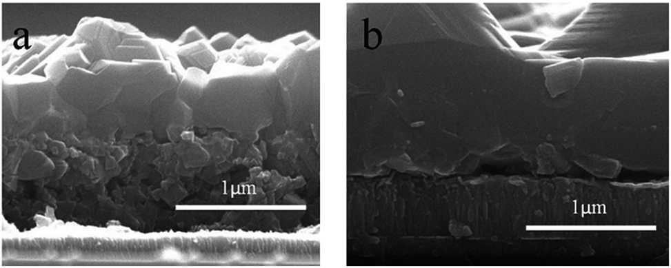 | ||
| Fig. 7 (a) Cross-section SEM images of a CIGSe film grown with (a) low Se and (b) high Se vapor pressure. Reprinted with permission from ref. 69, Copyright 2012 Royal Society of Chemistry. | ||
Cui and his group71 introduced a process named as air stable ink rolling (AIR) to produce thin film CuInS2 solar cells. This approach benefits from the use of rather low-cost precursors and an air-stable deposition method. The ink for CuInS2 comprised of copper acetylacetonate (Cu(acac)2), indium acetylacetonate (In(acac)3) and elemental S dissolved in pyridine which is significantly less toxic compared to hydrazine. In this process, sulfur vulcanization with acetylacetonate provides the opportune viscosity and wetting properties for film processing. Films prepared by this approach were subsequently pre-baked at a temperature of 370 °C in air to burn off the organics and form a stack of Cu–In oxide layers. The precursor oxide films were then converted to CuInS2 by a final sulfurization step in a bomb. The main deficiency of this approach was a poor control over the morphology and the film disruption induced during the sulfurization process resulting in solar cells with a low shunt resistance. Solar cells with PCEs of 2.15% were obtained after a post-KCN etching.
Apart from pyridine, other organic solvents with short ligands and strong coordinating properties were used to form an inexpensive and thermally degradable molecular precursor solution. For instance, a combination of butylamine and propionic acid was used to fabricate CuInS2 nanocrystalline solar cells based on an in situ synthesis and film deposition route.72 The attractive aspects of this approach are the simplicity of the process as well as a relatively low sintering temperature (<300 °C) used for the fabrication of solar cells. The drawbacks to this approach are however the poor stability of the precursor solution and a disordered film morphology.28Fig. 8 shows a scanning electron microscopy (SEM) image of a CuInS2 nanocrystal film prepared by the above approach. A detailed transport study of solar cells fabricated by this approach indicated a low carrier mobility of the CuInS2 nanocrystal films, limiting the conversion efficiency to an absorber thickness smaller than 200 nm.28 The use of an interpenetrating nanoscale heterojunction cell structure is expected to bypass the limitation of poor carrier collection at larger thicknesses.
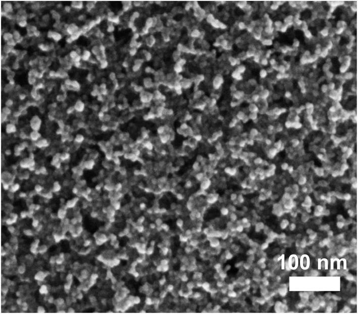 | ||
| Fig. 8 (a) SEM top view image of a CuInS2 NC film formed by an in situ deposition of precursor solution, sintered at a temperature of 270 °C. Reproduced with permission from ref. 28, Copyright 2013, Wiley VCH. | ||
Pan et al.73 used a reaction of butylamine with carbon disulfide (CS2) to synthesize butyldithiocarbamic acid (BDCA) that could efficiently dissolve a number of different metal oxides. Fig. 9 shows the reaction mechanism of butylamine with CS2 and the following reaction with a metal oxide, forming different thermally degradable metal–organic molecular precursor solutions. Solar cells fabricated by the selenization of films processed from a butyldithiocarbamic acid-based ethanol solution showed PCEs exceeding 10%,74 which are currently the highest reported performances for hydrazine-free molecular precursor-based CIGSe solar cells. Furthermore, the nontoxic ink formulation and the stability of the precursor solution over the course of months underscore the importance of the work reported by Pan et al.
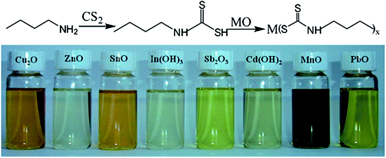 | ||
| Fig. 9 (Top) Reaction mechanism of a metal oxide with butyldithiocarbamic acid. (Bottom) Digital photograph of various metal oxides dissolved in chloroform with the aid of butylamine and carbon disulfide (∼0.35 M metal concentration). Reprinted with permission from ref. 73, Copyright 2012 American Chemical Society. | ||
Another common approach to fabricate chalcopyrite solar cells is based on the spray deposition technique. Typically, an aqueous precursor solution containing chloride metal salts along with thiourea as the sulfur source, in the case of CuInS2,75–77 and selenourea as the Se source, in the case of CuInSe2,78,79 has been used. The deposition temperature is typically around 250–400 °C, which is a lower temperature compared to the temperatures used for sulfurization or selenization. One attractive application of spray deposition is to allow fabrication of three-dimensional (3D) nanocomposite cell structures. Based on a chemical spray deposition and incorporating the CuInS2 nanocrystals into the matrix of In2S3/nanocrystalline anatase TiO2, Goossens et al.80 reported solar cells with device efficiencies of about 5% (see Fig. 10).
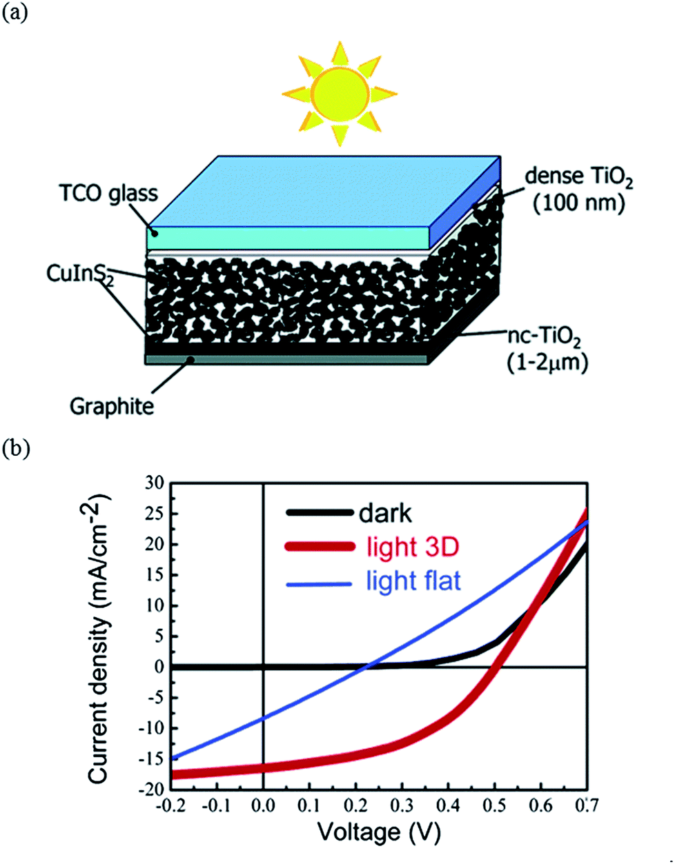 | ||
| Fig. 10 (a) Schematic picture of a nanocomposite 3D solar cell, and (b) J–V characteristics of the 3D solar cell based on a TiO2/In2S3/CuInS2 nanocomposite. Reprinted with permission from ref. 80, Copyright 2005, American Chemical Society. | ||
A number of studies have reported the synthesis of single source organometallic precursors for deposition of ternary CuInS2 and CuInSe2 thin films.81–84 Hirpo et al.81 first described the synthesis of the compound (PPh3)2CuIn(SEt)4 to prepare the ternary CuInX2 (X = S or Se) semiconductors. This compound comprises a copper(I) ion bound to two triphenylphosphine ligands, an indium(III) ion with two terminal ethanethiolate ligands, and two ethanethiolate ligands coordinated between the metal centers.81,82 The solubility of this compound in common organic solvents and the low decomposition temperature (<250 °C) make it an attractive candidate for spray pyrolysis deposition.81 Banger et al.82–84 have further developed the synthesis and deposition of single source precursors for ternary CuInX2 semiconductors. Also, solar cells with an efficiency of 6.7% were reported using the single-source precursor of (PPh3)2CuIn(SEt)4 and based on an aerosol-assisted chemical vapor deposition.85
A brief summary of the reports discussed in this section, dealing with deposition from the molecular-based precursor solutions, is presented in Table 2.
| Year | Absorber | J sc (mA cm−2) | V oc (mV) | FF (%) | PCE (%) | Deposition and solvent | Post-treatment | Description | Ref. |
|---|---|---|---|---|---|---|---|---|---|
| a n.a. = Not available, * ethylene glycol. | |||||||||
| 2013 | Cu(In,Ga)(S,Se)2 | 32.6 | 623 | 75 | 15.2 | Spin-coating, hydrazine | 540 °C (heat treatment under an inert atmosphere) | Hydrazinium precursors | 49 |
| 2012 | CuIn(S,Se)2 | 20.63 | 381 | 48.7 | 3.8 | Spin-coating, EA/DMSO | 400 °C (selenization) | Non-hydrazine solutions from hydrazinium precursors | 63 |
| 2005 | Cu(In,Ga)Se2 | 27.2 | 404 | 61 | 6.7 | Doctor-blading, alcoholic solvent | 550 °C (selenization in a Se/N2 atm.) | Metal-nitrates and metal-halides | 64 |
| 2013 | CuInGaS2 | 17.0 | 787 | 61.9 | 8.28 | Spin-coating, methanol | 500 °C (sulfurization in a H2S/N2 atm.) | Metal-nitrate salts | 67 |
| 2011 | CuInxGa1−xSe2 | 29.8 | 386 | 44 | 5.04 | Inkjet-printing, ethanol, EG,* and EA | 500 °C (selenization in a Se/H2/N2 atm.) | Metal-acetate and chloride salts | 68 |
| 2010 | CuInS2 | 18.49 | 320 | 37 | 2.15 | Ink-rolling, pyridine | 525 °C (sulfurization in a bomb) | Metal-acetylacetonate salts, air-stable process | 71 |
| 2010 | CuInS2 | 12.38 | 588 | 54.8 | 3.99 | Spin-coating, butylamine | 250 °C (heat treatment under an inert atmosphere) | Indium acetate, copper iodide, and thiourea | 72 |
| 2013 | CuIn(S,Se)2 | 27.64 | 561 | 65.0 | 10.1 | Spin coating ethanol with BDCA | 540 °C (selenization in a Se atm.) | A mixture of metallic oxide NPs | 74 |
| 2005 | CuInS2 | 17 | 530 | 55 | 5 | Spray-coating | Growth temperature 300 °C | Nanocomposite of TiO2/In2S3/CuInS2 | 80 |
3.2. Deposition from particulate-based solutions
In solution-based colloidal synthesis, it is possible to synthesize particles with a well-defined structure and high degree of purity. The nanoparticles offer a broad range of interesting tunable optical and electrical properties. Moreover, they offer excellent solution processing and their high reactivity is advantageous for phase transformation and film densification.86,87 In the synthesis of nanoparticles, it is very important to form particles with a uniform size and composition and with low levels of structural disorder. The use of organic ligands is generally required to properly control the kinetics of nucleation and growth during the synthesis. The organic ligands also play a key role in providing colloidal stability and later in assembling individual particles into a nanocrystal solid.88 The common organic surfactants are the long chain alkyl ligands like trioctylphosphite and oleylamine.89–91 Due to the insulating properties of these ligands that hamper an efficient transport between the nanoparticles, a complete removal of the organic ligands is crucial. The need for removal of bulky organic ligands can however result in generation of cracks and discontinuities in the nanoparticle film and may leave behind unwanted carbonaceous impurities and surface defects.55 To overcome the above issues, additional processing steps like ligand-exchange, heat treatment or chemical treatment are usually necessary.90,92–94In this section, we review the most recent work employing colloidal nanoparticle solutions for fabricating CIGS and chalcopyrite-based thin film solar cells. Table 3 presents a summary of some selected results along with information for the corresponding device parameters and preparation details. The section is sub-categorized into the use of (a) single phase, (b) binary or multi-phase particles as starting precursors for the film deposition. The discussion on the chemistry and properties of inorganic nanoparticles is not the purpose of this review. For detailed information, the reader is urged to refer to the number of excellent reviews that comprehensively address the mechanism of growth and the properties of inorganic nanoparticles.95–97
| Year | Absorber | J sc (mA cm−2) | V oc (mV) | FF (%) | PCE (%) | Deposition and solvent | Post-treatment | Description | Ref. |
|---|---|---|---|---|---|---|---|---|---|
| a n.a. = Not available., NPs = nanoparticles, OLA = oleylamine, TBP = tributylphosphine. | |||||||||
| 2008 | CuInSe2 | 25.8 | 280 | 39 | 2.82 | Drop-casting | 450–550 °C (selenization in a Se/Ar atmosphere) | CuInSe2 NPs (CuCl, InCl3 and Se in OLA) | 101 |
| 2009 | Cu(In1−xGax)(S1−ySey)2 | 23.7 | 455 | 51.5 | 5.5 | Drop-casting, toluene | 500 °C (selenization in a graphite box) | Cu(In1−x,Gax)S2 NPs (metal-chlorides and S in OLA) | 90 |
| 2013 | Cu(In,Ga)(S,Se)2 | 28.8 | 630 | 65.7 | 12 | Doctor-blading, hexanethiol | 500 °C (selenization in a graphite box) | Cu(In1−x,Gax)S2 NPs (metal(acac) salts and S in OLA) | 102 |
| 2010 | CuInSe2 | 16.3 | 410 | 46 | 3.1 | Spray-coating | n.a. | CuInSe2 NPs (metal-chlorides and Se in a mixture of OLA and TBP) | 104 |
| 2000 | CuInSe2 | 37.5 | 430 | 65.5 | 10.56 | Spray-coating, aqueous dispersion | 440 °C (selenization in a H2Se/N2 atm.) | Sub-micron sized Cu–In alloy particles (melt atomization technique) | 111 |
| 2003 | CuIn1−xGaxSe2 | 37.3 | 520 | 71 | 13.6 | Printing | 420–450 °C (reduction and selenization in H2/N2 and H2Se/N2 gas) | A mixture of oxide NPs (chemical approach) | 113 |
| 2011 | CuInSe2 | 34.3 | 352 | 57 | 7.0 | Doctor-blading | 550 °C (selenization in a Se/N2 atm.) | Citrate-capped Cu11In9 NPs (NaBH4-assisted chemical reduction) | 86 |
| 2012 | CuInSe2 | 33.7 | 440 | 55 | 8.2 | Drop-casting | 530 °C (selenization) | NPs of CuInSe2, CuSe, Cu2−xSe, and In2O3 (microwave-assisted synthesis) | 119 |
One of the first reports on the use of colloidal nanoparticles in solar cells was by Guo et al.,101 reporting solar cells with a PCE of 3.2% based on a CuInSe2 nanoparticle ink. Oleylamine was used as the capping agent during the synthesis and nanoparticles were dispersed in toluene. The nanocrystals were successfully sintered to micrometer large crystalline grains through an annealing step at temperatures of 450–550 °C under Se vapor. To remove the organic capping molecules prior to selenization, films were annealed under a flow of argon gas at 500 °C. The selenization however caused the inclusions of void space in the absorber film, imposing a major constraint on the photovoltaic performance. One year later and based on the same synthesis approach, Guo et al. improved the efficiencies to over 5% using sulfur based nanoparticular inks, i.e. CuInS2 and Cu(In1−xGax)S2 instead of CuInSe2. This exchange significantly promoted the volume expansion during the selenization process and led to the formation of a denser absorber film (see Fig. 11).90 Quaternary CIGS nanoparticles were designed instead of ternary sulfide and selenide nanoparticles to facilitate band-gap engineering. Most recently, hexanethiol based ink in combination with NaCl treatment yielded a 12% efficient Cu(In,Ga)(S,Se)2 nanocrystal-based solar cell.102 The positive influence of Na inclusion was attributed to an improved microstructure, substantially reducing recombination losses.
 | ||
| Fig. 11 FE-SEM images of (a) CuInS2 nanocrystal film prepared on a Mo-coated soda lime glass substrate by drop-casting of nanocrystal ink and (b) after selenization at 500 °C for 45 min showing the formation of large crystalline grains and high compactness of the film. Reprinted with permission from ref. 90, Copyright 2009 American Chemical Society. | ||
As mentioned above, post-thermal selenization poses additional costs and technological impediments on the production process. From this standpoint, it is important to highlight the work by Korgel et al.,103 reporting colloidal CuInSe2 nanoparticle based solar cells without high temperature sintering. By spray-depositing CISe and CIGSe nanoparticles and by optimizing the device structure, solar cells with PCEs of up to 3.1% were reported (see Fig. 12).104,105 In this study, the conventional Mo back contact was replaced by gold (Au) to ensure a good ohmic contact to the absorber layer. The general consensus is that a thin layer of MoSe2, which is being formed during the crystallization process at high temperatures, subjects Mo to a selective electrical contact for CISe and CIGSe absorber layers.106,107
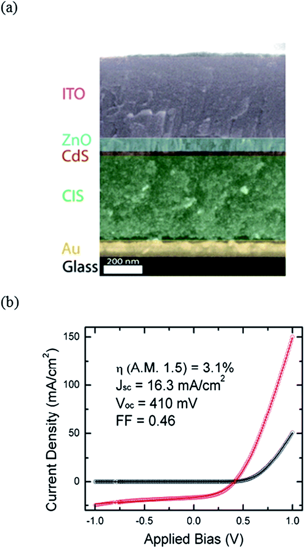 | ||
| Fig. 12 (a) Cross-sectional SEM picture of a solar cell fabricated by spray-depositing of CuInSe2 nanoparticles without the use of any high temperature processing (reprinted with permission from ref. 105, Copyright 2012 Elsevier B.V.) and (b) the corresponding current–voltage characteristics measured under 100 mW cm−2 AM1.5G (reprinted with permission from ref. 104, Copyright 2010 Optical Society of America). | ||
The strategy to design new capping agents is an attractive way to improve the performance of nanocrystal-based solar cells without high temperature processing. All the experiments mentioned above have focused on the use of oleylamine as the capping agent. In attempting to improve the transport properties and functionality of nanoparticle based solar cells, different inorganic moieties including inorganic metal chalcogenide–hydrazinium complexes (MCC), S2−, HS−, and OH− were adopted.89 However, no improvement over the oleylamine-capped nanoparticles was found for MCC-capped CISe nanoparticles, which in addition had the drawback of using toxic and highly reactive hydrazine. The above study nevertheless showed that further studies on understanding and the engineering of novel ligands can facilitate low-temperature processed nanocrystal-based solar cells with high performance.
As the line of research continued, a significant portion of the research was devoted to the preparation of particles via chemical means. Kapur et al.113 obtained high efficiency devices with PCEs exceeding 13% using a mixture of oxide based nanoparticles, which were reduced and selenized in H2/N2 and H2Se/N2 gas. The intermetallic Cu–In particles were also synthesized through a chemical reduction method.114–117 The inorganic compound sodium borohydride (NaBH4) was commonly used as the reducing agent. NaBH4 is a mild and inexpensive reagent whose reactivity is enhanced in the presence of certain organic and inorganic compounds.118 However, efforts to fabricate solar cells based on NaBH4-assisted chemical reduction led to fairly low efficiency devices (≤1.4%). The problem was mainly related to the high level of porosity and structural free volume in the films.114,116 The breakthrough in this approach was reported by Kind et al.,86 demonstrating 7% efficient solar cells based on the deposition of citrate-capped Cu11In9 nanoparticles, followed by selenization under H2Se. The Cu11In9 particles with a diameter of 10–30 nm were prepared by a polyol-mediated synthesis, where an aqueous solution of NaBH4 was injected into a solution of CuCl2, InCl3, and disodium citrate hydrate in diethylene glycol (see Fig. 13 for the electron microscopy image of as-prepared nanoparticles). The role of disodium citrate was not only to control the nucleation and stability of the Cu11In9 nanoparticles, but also to effectively suppress the particle-to-particle agglomeration. Recently, organic free Cu–In alloy nanoparticle precursor ink was prepared by NaBH4-assisted chemical reduction and used to fabricate a CuInSe2 absorber layer, but only solar cells with a low PCE of 3.92% were reported.87
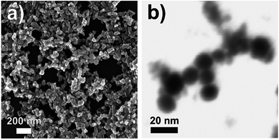 | ||
| Fig. 13 Electron microscopy of citrate-capped Cu11In9 nanoparticles: (a) SEM overview image, and (b) detailed bright-field STEM image. Reprinted with permission from ref. 86, Copyright 2011 American Chemical Society. | ||
Another interesting approach was reported by Jeong et al.,119 who used a mixture of nanoparticles of CuInSe2, CuSe, Cu2−xSe, and In2O3 to fabricate CuInSe2 devices with efficiencies of up to 8.2%. The multiphase nanoparticles in this study were produced via a microwave-assisted solvothermal synthesis. In microwave processing, due to the tendency of particles to precipitate in a fast and nearly simultaneous manner, the synthesis of particles with small size and narrow size distribution is possible.95
Another interesting concept was introduced by Min Lim et al.,120 reporting the formation of quaternary CuInSxSe1−x nanoparticles via chemical welding of binary CuSe and In2Se3 nanoparticles at room temperature. Contrary to most reports, the coalescence and sintering of particles were performed in the liquid phase, and imposed by oppositely charging the CuS and In2S3 nanoparticles (schematically outlined in Fig. 14). To establish opposite charges on the particle surface, the nanoparticles were synthesized in the presence of polyacrylic acid (PAA) and polydiallyldimethylammoniumchloride (PDDA), respectively, for CuS and In2S3 nanoparticles.
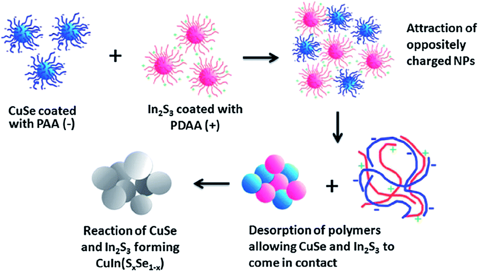 | ||
| Fig. 14 A schematic diagram representing the formation of CuInSxSe1−x nanoparticles through electrostatically induced coalescence and sintering of binary CuSe and In2Se3 nanoparticles. Reprinted with permission from ref. 120, Copyright 2013, The Royal Society of Chemistry. | ||
Most of the studies discussed so far employed relatively crystalline nanoparticles. Nevertheless, due to the high melting temperature of crystalline particles, they might not be necessarily the best choice for device fabrication. Ahn et al.121,122 reported the synthesis and utilization of amorphous Cu–In–Se nanoparticles, aiming to benefit from the lower melting temperatures of such particles to assist an effective sintering during a post-thermal treatment. CuInSe2 films formed from amorphous Cu–In–Se nanoparticles showed dense morphologies for particles modified by chelate complexation with ethanolamine. Recently, they demonstrated devices with efficiencies of up to 7.9% from modified amorphous nanoparticles.123
3.3. Deposition from nanoparticles/precursor solution
Hybrid inks are interesting from the perspective of combining the advantages of particulate-based and molecular-based precursor solutions. In a hybrid ink of nanoparticles mixed into a precursor, the precursor solution can be used as a medium to provide effective binding between nanoparticles. Further, the particles can act as nucleation sites to promote grain growth and film densification. Cho et al.124 developed a hybrid ink using a mixture of colloidal CuS nanoparticles and an indium precursor solution to form a dense layer of CuInSe2, demonstrating solar cells with efficiencies of over 6% after selenization. Similar device efficiencies were reported by Cai and coworkers based on spray deposition from a hybrid ink containing molecular precursors of CuCl2, InCl3, and thiourea mixed with CuS and In2S3 nanoparticles.125 The inclusion of CuS and In2S3 nanoparticles in the precursor solution led to a substantial improvement in device performance, mainly as a result of increased Jsc and Voc. The comparison between the J–V characteristics of devices made from a precursor solution and a nanoparticle/precursor solution is shown in Fig. 15.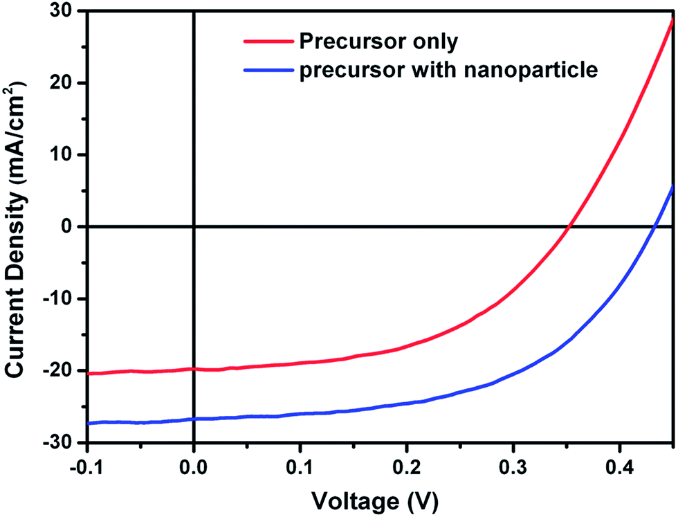 | ||
| Fig. 15 J–V curve of the device fabricated from a nanoparticle incorporated precursor film (blue) and a precursor film without nanoparticles (red). Reprinted with permission from ref. 125, Copyright 2013 American Chemical Society. | ||
3.4. Hybrid organic/inorganic solar cells
Inorganic semiconductor nanocrystals were investigated in combination with organic molecules or nanostructure metal oxides to combine attractive features of both classes of materials for applications like photodetectors and photovoltaics.126–128 Because of the high carrier mobility and tunable absorption properties, inorganic NCs are attractive to be used as electron accepting or donating materials for organic solar cells. These attractive features can be beneficial when combined with the low temperature processing of organic solar cells.129CuInS2 and CuInSe2 nanoparticles were used as electron acceptors130,131 or electron donors132 in combination with different polymers or organic small molecules to form a bulk-heterojunction solar cell structure. The semiconducting properties of CuInS2 can be modified, depending on the ratio between Cu and In, to a p-type (Cu/In > 1) or an n-type (Cu/In < 1) semiconductor.133
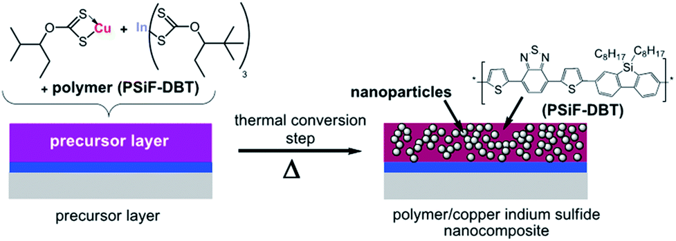
In a blend of colloidal CuInS2 nanoparticles with conjugated polymers, the process of charge transfer was observed by photoluminescence and photo-induced absorption spectroscopic measurements.134,135 However, due to the limitations imposed by the presence of organic ligands as well as surface traps on the nanoparticles, fairly low efficiencies were reported (PCEs < 1%).132,134–136 The intricacy of controlling the morphology is another decisive factor, influencing the performance of hybrid solar cells. Such issues could be largely overcome by an in situ formation of the inorganic nanocrystals directly inside an organic matrix. This approach has the advantages of eliminating the need for a separate nanoparticle synthesis and the use of an organic capping ligand.137,138 The in situ formation of CuInS2 nanoparticles in an organic semiconductor was described by Rath et al.139 and Maier et al.131 The process reported by Rath et al. is schematically described in Fig. 16, in which the CuInS2 nanoparticles were directly formed in the matrix of the conjugated polymer, poly[(2,7-silafluorene)-alt-(4,7-di-2-thienyl-2,1,3-benzothiadiazole)] (PSiF-DBT), using easily thermally decomposable organometallic complexes, copper xanthates and indium xanthates. A mild annealing step at 200 °C was used to complete the fabrication of nanocomposite CuInS2/PSiF-DBT solar cells. A conversion efficiency of 2.8% was achieved, which is one of the highest efficiencies ever reported for polymer/CIS nanocomposite solar cells.
 | ||
| Fig. 16 Schematic representation of the polymer/CIS nanocomposite formation. Reprinted with permission from ref. 139, Copyright 2011, Wiley VCH. | ||
A summary of the solar cell results associated with the use of hybrid mixtures, i.e. nanoparticles/precursor and inorganic/organic, is given in Table 4.
| Year | Absorber | J sc (mA cm−2) | V oc (mV) | FF (%) | PCE (%) | Deposition and solvent | Post-treatment | Description | Ref. |
|---|---|---|---|---|---|---|---|---|---|
| a NPs = nanoparticles. | |||||||||
| NPs/precursor | CuInSe2 | 31.01 | 420 | 47.5 | 6.23 | Spin-coating | 530 °C (selenization) | CuS NPs and an indium precursor solution | 124 |
| NPs/precursor | CuIn(S,Se)2 | 26.7 | 430 | 53 | 6.15 | Spray-coating | 480–500 °C (selenization) | Molecular precursors of CuCl2, InCl3, and thiourea mixed with CuS and In2S3 NPs | 125 |
| Hybrid inorganic/organic | P3HT*/CuInSe2 | 0.56 | 440 | 30 | 0.7 | Spin-coating | Annealing at 220 °C | CuInSe2 nanocrystals mixed with P3HT weight ratio of 1:6 |
135 |
| Hybrid inorganic/organic | CuInS2/PSiF-DBT | 10.3 | 540 | 50 | 2.8 | Spin-coating | Annealing at 200 °C | In situ formation of CuInS2 NPs in polymer | 139 |
4. Solution processed kesterite solar cells
Kesterite-based compounds, i.e. Cu2ZnSnS4 (CZTS), Cu2ZnSnSe4 (CZTSe), and Cu2ZnSn(S,Se)4 (CZTSSe), are materials showing optical and electronic properties comparable to those of the chalcopyrite CuInS2, CuInSe2 and Cu(In, Ga)(Se, S)2 materials, however with the advantage of being composed of only abundant and economical elements.31 Among all, CZTS with an optimal bandgap of 1.5 eV and a large absorption coefficient of 104 cm−1 is one of the best absorber materials for solar cell mass production.140 Despite the promising potential, there is still a significant performance gap between the best kesterite-based and chalcopyrite solar cells (see Fig. 1). The reason can be found in manifold complexities related to the crystal structure, stoichiometry, point defects and morphology of kesterite. Due to the narrower existence region of the kesterite phase compared to the analogous chalcopyrites, secondary phases and point defects are a serious challenge in this material system.23,141Fig. 17 compares the calculated stable chemical potential range for chalcopyrite CuInSe2 and kesterite Cu2ZnSnS4, showing the more complicated limit to the chemical potential region for the latter compound.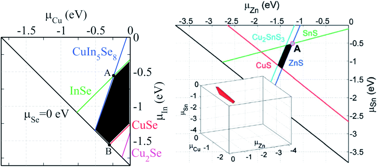 | ||
| Fig. 17 The calculated chemical potential diagram of (left) CuInSe2 in the (μCu, μIn) plane and (right) Cu2ZnSnS4 in a 2D Cu-rich plane (the stable 3D region is shown in the inset).24 The black area shows the chemical potentials under which CuInSe2 and Cu2ZnSnS4 are thermodynamically stable against different competing secondary compounds. Reprinted with permission from ref. 31 and 23, Copyright 2012 and 2013, Wiley VCH. | ||
In order to close the performance gap with CIGSSe, further applied and theoretical studies are necessary to understand the underlying interfaces and corresponding defects of the CZTSSe system. Interestingly, the presently highest efficiency CZTSSe devices are based on fabrication via solution-processing methods. One of the major issues is the more volatile mix of elements (e.g. Sn) in the CZTSSe system, causing a severe limitation for the vacuum based techniques requiring post-thermal treatment at temperatures >400 °C.142,143 Although this problem is largely resolved by heat treatments under different chalcogen-containing (e.g. Sn) atmospheres,144 the device efficiencies are still below those prepared by liquid-based processing.
4.1. Hydrazine solution processing of CZTS(e)
Currently, there are two types of hydrazine based solution processing routes: one is based on a hybrid mixture of nanoparticles and a precursor solution, which involves undissolved Zn particles and truly dissolved precursor solutions,145 and another is a purely molecular based approach which involves all the chalcogenides fully dissolved at a molecular level.146 Both of these approaches exhibited highly efficient solar cells. Originating from the previous works on hydrazine processed CIGSSe absorbers, Mitzi et al.145 demonstrated the fabrication of CZTSSe thin film solar cells with 11.1% power conversion efficiency using a hydrazine-based hybrid approach. Quite recently, by optimizing the thickness of the CdS and transparent-conducting layers, Mitzi et al. improved the device efficiency to 12.0%.147 Until today, this performance holds the highest reported efficiency for this material system. Another hydrazine-based approach was reported recently by Yang et al.146 In this study, the hydrazine derivatives were designed to allow the effective incorporation of zinc compounds into hydrazine solution, forming a CZTS precursor solution that is homogeneous at the molecular level. Based on a deposition from this precursor solution and a subsequent selenization process, a solar cell with an efficiency of 8.08% was produced.4.2. Non-hydrazine solution processing of CZTS(e)
Although among all available fabrication routes including both vacuum and non-vacuum based techniques, the hydrazine based approach has yielded the highest efficiency kesterite solar cells, as previously mentioned, the explosivity and toxicity of hydrazine extremely limit its application in large scale production.148 It is hence essential to develop a relatively simple precursor route using less toxic solvents with comparable performance to those made from hydrazine based approaches.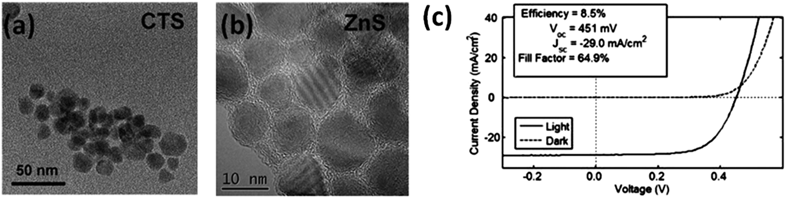 | ||
| Fig. 18 TEM pictures of (a) CTS and (b) ZnS nanoparticles and the corresponding (c) J–V curves of CZTSSe devices. Reprinted with permission from ref. 151, Copyright 2012 American Chemical Society. | ||
Similar to the particulate-based methods used for fabrication of CIGS devices, a mixture of metallic and metallic chalcogenide nanoparticles was used to form kesterite CZTS films. Based on a precursor solution containing a powder mixture of Cu2S, Zn, Sn, and S nanoparticles dispersed in ethanol, Woo et al.156 reported the fabrication of CZTS solar cells with the highest PCE of 5.14%.
Despite all these promising reports, there are still some unsolved problems concerning the use of nanoparticles. One major issue is related to the carbon residues remaining in the final film after high temperature selenization or sulfurization, promoting formation of a small-grained inter-layer in the film. Another problem is the trade-off between impurities left after the decomposition of the ligands and the need for high-quality dispersion precursors. To address the above issues, Carrete et al.157 developed a multistrategy ligand exchange approach in the solution phase to remove the organic ligands. In this work, they introduced an antimony salt to displace the organic ligands from the surface of CZTS nanoparticles (see Fig. 19, a schematic picture describing the ligand-exchange). Moreover, antimony effectively reduced the material melting point that promoted the diffusion-controlled crystallization. With an automated pulsed spray deposition followed by selenization treatment, homogeneous and carbon-free CZTSSe thin films were fabricated.
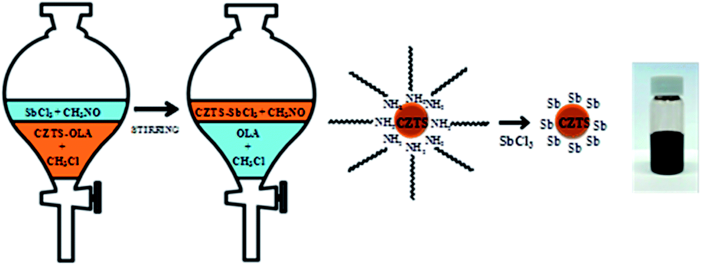 | ||
| Fig. 19 Schematized view of the procedure representing the ligand-exchange of the long-chain OLA ligand with an inorganic salt SbCl3. Reprinted with permission from ref. 157, Copyright 2013 American Chemical Society. | ||
The current knowledge of particle synthesis allows the preparation of CZTS and CZTSe nanoparticles with a fine crystal structure and favorable chemical composition in various organic solvents; this makes the direct deposition of such nanoparticles at low processing temperatures feasible without high temperature selenization or sulfurization. The ultimate goal of this approach is to develop nanoparticle inks to deposit inorganic thin films under ambient or mild processing conditions, ideally in a high-throughput printing process, like a roll-to-roll process on flexible substrates. Recently, there have been some reports focusing on low temperature processing of CZTS nanoparticles. Korgel group reported a device efficiency of 0.23% utilizing the Au/CZTS/CdS/ZnO/ITO device structure without any post-thermal annealing process.152 The cause of such low device efficiency is largely due to the existence of insulating organic ligands on the large surface areas of CZTS nanoparticles, inhibiting the effective charge transport between the particles. Exchanging the long chain of the capping agent oleylamine by the short ligand pyridine and employing a solar cell architecture of ITO/CZTS/PCBM/Ca/Al, Saha et al.158 demonstrated CZTS solar cells with an improved PCE of 0.9%. Further improvement in device efficiencies can be expected by implementing effective approaches to overcome the presence of insulating organic ligands and to passivate the various trap sites on the particle surface.
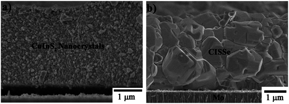
 | ||
| Fig. 20 Cross-sectional SEM pictures of (a) the as-deposited precursor-based film and (b) the corresponding selenized sample. Reprinted with permission from ref. 160, Copyright 2012 Elsevier B.V. | ||
Wang et al.159 employed a molecular precursor solution comprised of a mixture of binary metallic precursor oxides of Cu2O, ZnO, and SnO dissolved in a mixture of ethanol solution with butyldithiocarbamic acid, a similar method to the one developed for fabrication of high quality CIGSSe layers.73,74 By optimizing the composition of CZTSe, solar cells with a device efficiency of 6.03% have been achieved. The advantage of this approach is the use of volatile less toxic ethanol as the main solvent and the formation of the CZTS phase at relatively low temperatures of 320 °C without any formation of binary and ternary chalcogenide phases.
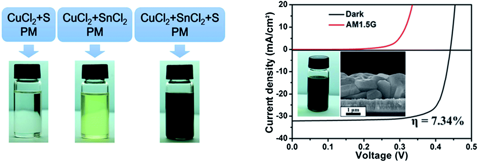 | ||
| Fig. 21 (a) The preparation schematic and photographs of the parallel experiments to synthesize the CTS nanoparticles and (b) the I–V characteristic of a CZTSSe solar cell prepared by using a hydrazine-free hybrid particles/precursor solution (the inset shows the corresponding cross-section SEM image of the selenized CZTSSe layer). Reprinted with permission from ref. 162, Copyright 2013, The Royal Society of Chemistry. | ||
5. Summary and outlook
Depending on the method of preparation, Fig. 22 compares the absolute efficiency of the most efficient solution processed chalcopyrite solar cells published within the last five years, indicating a clear trend to better device efficiencies. The record published PCE of 15.2% based on the pure solution deposition,49 and the certified 17.1% printed CIGSe solar cell on flexible foil announced by Nanosolar,163 show the promising path of this technology, bridging the performance gap with the highest efficiency vacuum-based devices with a PCE of 20.4%.5 A similar progress can be also realized in the field of solution processed kesterite solar cells with reported maximum efficiencies of 10.2% for hydrazine-free processes and 12% for the hydrazine-based approach. Although the most efficient solution processed solar cells still belong to the category of hydrazine-based devices, with plenty of studies recently concentrating on non-hydrazine based devices, there has been also a rapid progress towards efficient hydrazine-free solar cells. As shown in Fig. 22, this progress can be clearly seen for both particulate and precursor-based devices. By summarizing the results in Tables 2–5, one can see that most of the studies employ high temperature selenization or sulfurization, where only sporadic studies reported solar cells without a high temperature crystallization process. The complex post-treatments and high temperature processing routes are the important cost-driving factors for the production of solar cell technology. The high temperature routes impose not only high energy costs, but also prohibit the use of cheap substrates needed for the low-cost solar cell fabrication. With further emphasis on the low temperature processing routes, the green formulations and ongoing focus on kesterite solar cells as an excellent replacement containing only earth-abundant elements, printable multicomponent inorganic inks can lead to inexpensive fabrication for light absorbing thin films. To make this possible, significant amount of investigation seems to be still necessary to unravel the complexity in the synthesis chemistry, dissolution mechanisms, drying kinetics and phase formation of thin films and their relationship to various loss mechanisms in photovoltaic devices. The pace of development can be accelerated with the emergence of new concepts and an increasing attention on hybrid structures.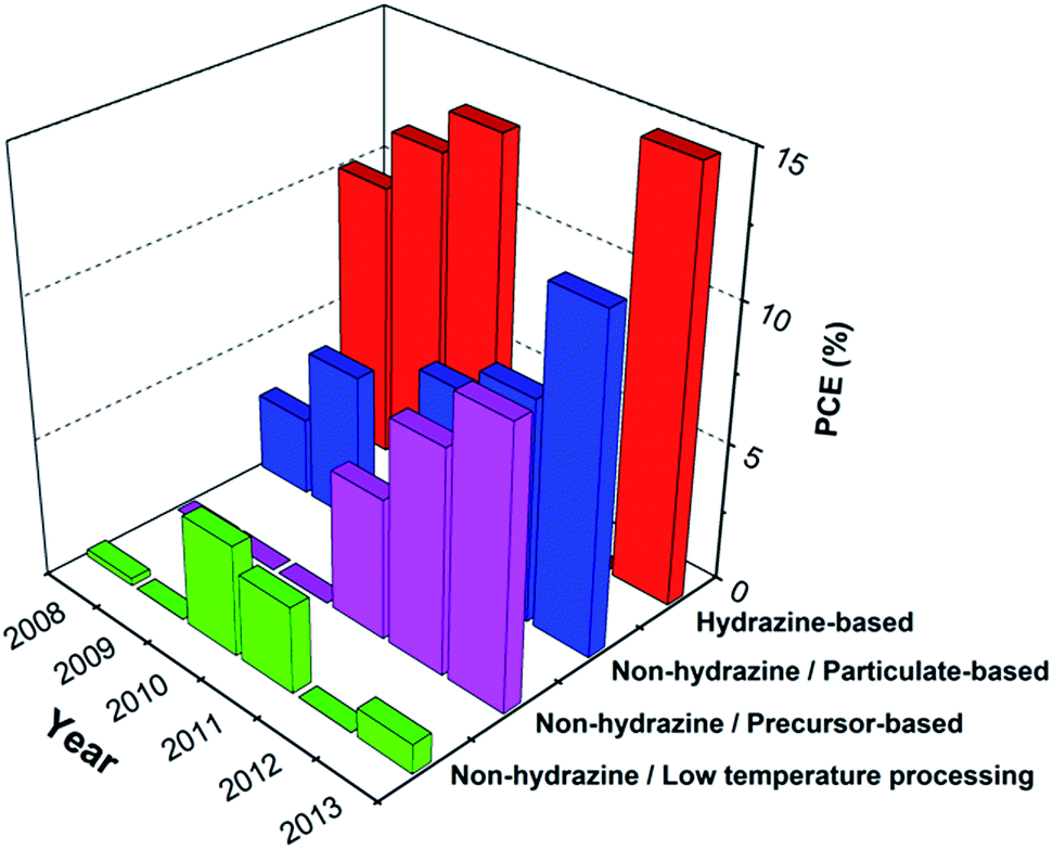 | ||
| Fig. 22 Comparison of the absolute efficiency of most efficient hydrazine-based (red), non-hydrazine/particlulate-based (blue), non-hydrazine/precursor-based (pink), and non-hydrazine/low temperature processed (green) solution processed chalcopyrite solar cells, published during the last five years. | ||
| Year | Absorber | J sc (mA cm−2) | V oc (mV) | FF (%) | PCE (%) | Deposition and solvent | Post-treatment | Description | Ref. |
|---|---|---|---|---|---|---|---|---|---|
| n.a. = not available, OLA = oleylamine. | |||||||||
| 2013 | CZTSSe | 34.8 | 498 | 69.5 | 12.0 | Spin-coating, hydrazine | n.a. | n.a. | 147 |
| 2012 | CZTSSe | 34.5 | 460 | 69.8 | 11.1 | Spin-coating, hydrazine | >500 °C (annealing with varying the concentration of S in the atm.) | A mixture of metallic chalcogen precursors and Zn NPs | 145 |
| 2012 | CZTSSe | 32.3 | 409 | 61.0 | 8.1 | Spin-coating, hydrazine | 500 °C (under different chalcogen vapor S, S + Se and Se) | A mixture of metallic chalcogen precursors | 146 |
| 2012 | CZTSSe | 32.8 | 459 | 68.0 | 10.2 | n.a. | n.a. | n.a. | 154 |
| 2012 | CZTSSe | 29 | 451 | 64.9 | 8.5 | Spin-coating, hexanethiol | Selenization in a graphite box | Binary and ternary NPs of CTS, ZnS, and SnS | 151 |
| 2012 | CZTGeSSe | 28.1 | 464 | 62.0 | 8.4 | Doctor-blading, hexanethiol | 500 °C (selenization in a graphite box) | CZTGeSSe particles in OLA | 155 |
| 2012 | CZTS | 18.9 | 517 | 52.8 | 5.1 | Spin-coating, ethanol | 400–530 °C (sulfurization in N2 + H2S (5%) atm.) | Nanosized powder of Cu2S, Zn, Sn, and S (milling process) | 156 |
| 2009 | CZTS | 1.95 | 321 | 37.0 | 0.23 | Spray-coating, chloroform | No annealing | Cu(acac)2, zinc acetate SnCl2 and S in OLA | 152 |
| 2012 | CZTS | 5.30 | 390 | 43.0 | 0.90 | Spin-coating, toluene | No annealing (solid state ligand exchange by pyridine) | CuCl2, ZnCl2, SnCl4 and S in OLA | 158 |
| 2013 | CZTSSe | 33.7 | 440 | 55 | 7.5 | Doctor-blading, DMSO | 540 °C (selenization in a home-made halogen-lamp-heated furnace) | Cu(OAc)2, ZnCl2, SnCl, and thiourea in DMSO, binder-free | 160 |
| 2013 | CZTS | 17.5 | 180 | 32.8 | 6.0 | Spin-coating, ethanol with BDCA | 540°C (samples and Se powder were sealed in a hard test tube) | A mixture of metallic oxide NPs | 159 |
| 2013 | CZTSSe | 32.6 | 457 | 66.1 | 7.4 | Spin-coating, PM | 450–550 °C (under different chalcogen vapors S, S + Se and Se) | CTS particles mixed with ZnCl2 | 162 |
Acknowledgements
The authors would like to acknowledge the funding of the Deutsche Forschungsgemeinschaft (DFG) through the Cluster of Excellence Engineering of Advanced Materials. They also acknowledge BAYER Technology Services and Solar-Fabrik AG for financial support.References
- National Renewable Energy Laboratory, NREL. National solar energy roadmap. In Series Management Reports. 2007, NREL/MP-520-41733/41741.
- C. Candelise, M. Winskel and R. Gross, Prog. Photovolt: Res. Appl., 2012, 20, 816–831 CrossRef.
- C. J. Brabec, Sol. Energy Mater. Sol. Cells, 2004, 83, 273 CrossRef CAS.
- P. Jackson, D. Hariskos, E. Lotter, S. Paetel, R. Wuerz, R. Menner, W. Wischmann and M. Powalla, Prog. Photovolt: Res. Appl., 2011, 19, 894–897 CrossRef CAS.
- A. Chirilă, P. Reinhard, F. Pianezzi, P. Bloesch, A. R. Uhl, C. Fella, L. Kranz, D. Keller, C. Gretener, H. Hagendorfer, D. Jaeger, R. Erni, S. Nishiwaki, S. Buecheler and A. N. Tiwari, Nat. Mater., 2013, 12, 1107–1111 CrossRef PubMed.
- C. J. Hibberd, E. Chassaing, W. Liu, D. B. Mitzi, D. Lincot and a. N. Tiwari, Prog. Photovoltaics Res. Appl., 2010, 18, 434–452 CrossRef CAS.
- V. S. Saji, I.-H. Choi and C.-W. Lee, Sol. Energy, 2011, 85, 2666–2678 CrossRef CAS.
- J.-F. Guillemoles, P. Cowache, A. Lusson, K. Fezzaa, F. Boisivon, J. Vedel and D. Lincot, J. Appl. Phys., 1996, 79, 7293 CrossRef CAS.
- M. A. Green, K. Emery, Y. Hishikawa, W. Warta and E. D. Dunlop, Prog. Photovolt: Res. Appl., 2013, 21, 827–837 CrossRef.
- R. Scheer, H.-W. Schock, Chalcogenide Photovoltaics: Physics, Technologies, and Thin Film Devices, WILEY-VCH Verlag & Co. KGaA 2011 Search PubMed.
- J. Nelson, The Physics of Solar Cells, Imperial College Press, London 2003 Search PubMed.
- A. Chirilă, S. Buecheler, F. Pianezzi, P. Bloesch, C. Gretener, A. R. Uhl, C. Fella, L. Kranz, J. Perrenoud, S. Seyrling, R. Verma, S. Nishiwaki, Y. E. Romanyuk, G. Bilger and A. N. Tiwari, Nat. Mater., 2011, 10, 857–861 CrossRef PubMed.
- U. Rau and H. W. Schock, Appl. Phys. A, 1999, 69, 131 CrossRef CAS.
- S. Siebentritt, Sol. Energy Mater. Sol. Cells, 2011, 95, 1471 CrossRef CAS.
- S. Siebentritt, M. Igalson, C. Persson and S. Lany, Prog. Photovoltaics Res. Appl., 2010, 18, 390 CrossRef CAS.
- U. Rau, K. Taretto and S. Siebentritt, Appl. Phys. A, 2008, 96, 221 CrossRef.
- M. Gloeckler, J. R. Sites and W. K. Metzger, J. Appl. Phys., 2005, 98, 113704 CrossRef.
- K. Taretto and U. Rau, J. Appl. Phys., 2008, 103, 094523 CrossRef.
- D. Schmid, M. Ruckh and H. W. Schock, Sol. Energy Mater. Sol. Cells, 1996, 41-42, 281 CrossRef.
- J. Li, D. B. Mitzi, V. B. Shenoy and V. B. Shenoy, ACS Nano, 2011, 5, 8613 CrossRef CAS PubMed.
- S.-H. Wei, S. B. Zhang and A. Zunger, Appl. Phys. Lett., 1998, 72, 3199 CrossRef CAS.
- M. J. Romero, H. Du, G. Teeter, Y. Yan and M. M. Al-Jassim, Phys. Rev. B: Condens. Matter Mater. Phys., 2011, 84, 165324 CrossRef.
- S. Chen, A. Walsh, X.-G. Gong and S.-H. Wei, Adv. Mater., 2013, 25, 1522 CrossRef CAS PubMed.
- S. Chen, X. G. Gong, A. Walsh and S.-H. Wei, Appl. Phys. Lett., 2010, 96, 021902 CrossRef.
- C.-H. Chung, S.-H. Li, B. Lei, W. Yang, W. W. Hou, B. Bob and Y. Yang, Chem. Mater., 2011, 23, 964 CrossRef CAS.
- J. Alvarez-García, E. Rudigier, N. Rega, B. Barcones, R. Scheer, a. Pérez-Rodríguez, a. Romano-Rodríguez and J. R. Morante, Thin Solid Films, 2003, 431–432, 122–125 CrossRef.
- E. Rudigier, I. Luck and R. Scheer, Appl. Phys. Lett., 2003, 82, 4370 CrossRef CAS.
- H. Azimi, T. Heumüller, A. Gerl, G. Matt, P. Kubis, M. Distaso, R. Ahmad, T. Akdas, M. Richter, W. Peukert and C. J. Brabec, Adv. Energy Mater., 2013, 3, 1589 CrossRef CAS.
- I. Oja, M. Nanu, a. Katerski, M. Krunks, a. Mere, J. Raudoja and a. Goossens, Thin Solid Films, 2005, 480–481, 82–86 CrossRef CAS.
- A.-J. Cheng, M. Manno, a. Khare, C. Leighton, S. a. Campbell and E. S. Aydil, J. Vac. Sci. Technol., A, 2011, 29, 051203 Search PubMed.
- A. Walsh, S. Chen, S.-H. Wei and X.-G. Gong, Adv. Energy Mater., 2012, 2, 400 CrossRef CAS.
- P. a. Fernandes, P. M. P. Salomé and a. F. da Cunha, Thin Solid Films, 2009, 517, 2519 CrossRef CAS.
- R. Ahmad, M. Distaso, H. Azimi, C. J. Brabec and W. Peukert, J. Nanopart. Res., 2013, 15, 1886 CrossRef.
- X. Fontané, L. Calvo-Barrio, V. Izquierdo-Roca, E. Saucedo, a. Pérez-Rodriguez, J. R. Morante, D. M. Berg, P. J. Dale and S. Siebentritt, Appl. Phys. Lett., 2011, 98, 181905 CrossRef.
- F. Hergert, R. Hock, a. Weber, M. Purwins, J. Palm and V. Probst, J. Phys. Chem. Solids, 2005, 66, 1903 CrossRef CAS.
- C. von Klopmann, J. Djordjevic and R. Scheer, J. Cryst. Growth, 2006, 289, 113 CrossRef CAS.
- A. Fischereder, T. Rath, W. Haas, H. Amenitsch, D. Schenk, A. Zankel, R. Saf, F. Hofer and G. Trimmel, ACS Appl. Mater. Interfaces, 2012, 4, 382 CAS.
- V. Izquierdo-Roca, A. Shavel, E. Saucedo, S. Jaime-Ferrer, J. Álvarez-García, A. Cabot, A. Pérez-Rodríguez, V. Bermudez and J. R. Morante, Sol. Energy Mater. Sol. Cells, 2011, 95, S83 CrossRef CAS.
- K. Topper, J. Bruns, R. Scheer, M. Weber, a. Weidinger and D. Bräunig, Appl. Phys. Lett., 1997, 71, 482 CrossRef CAS.
- F. Luckert, D. I. Hamilton, M. V. Yakushev, N. S. Beattie, G. Zoppi, M. Moynihan, I. Forbes, a. V. Karotki, a. V. Mudryi, M. Grossberg, J. Krustok and R. W. Martin, Appl. Phys. Lett., 2011, 99, 062104 CrossRef.
- J. Raudoja and M. Altosaar, Sol. Energy Mater., 2003, 79, 401 CrossRef.
- M. Burgelman, F. Engelhardt, J. F. Guillemoles, R. Herberholz, M. Igalson, R. Klenk, M. Lampert, T. Meyer, V. Nadenau, A. Niemegeers, J. Parisi, U. Rau, H. W. Schock, M. Schmitt, O. Seifert, T. Walter and S. Zott, Prog. Photovolt: Res. Appl., 1997, 5, 121–130 CrossRef CAS.
- A. Jasenek, U. Rau, V. Nadenau and H. W. Schock, J. Appl. Phys., 2000, 87, 594 CrossRef CAS.
- R. Knecht, M. S. Hammer, J. Parisi and I. Riedel, Phys. Status Solidi, 2013, 210, 1392–1399 CrossRef CAS.
- J. P. Leitão, N. M. Santos, P. a. Fernandes, P. M. P. Salomé, a. F. da Cunha, J. C. González, G. M. Ribeiro and F. M. Matinaga, Phys. Rev. B: Condens. Matter Mater. Phys., 2011, 84, 024120 CrossRef.
- S. Siebentritt and S. Schuler, J. Phys. Chem. Solids, 2003, 64, 1621 CrossRef CAS.
- O. Gunawan, T. K. Todorov and D. B. Mitzi, Appl. Phys. Lett., 2010, 97, 233506 CrossRef.
- S. Shirakata and T. Nakada, Thin Solid Films, 2007, 515, 6151–6154 CrossRef CAS.
- T. K. Todorov, O. Gunawan, T. Gokmen and D. B. Mitzi, Prog. Photovolt: Res. Appl., 2013, 21, 82–87 CrossRef CAS.
- J. B. Li, V. Chawla and B. M. Clemens, Adv. Mater., 2012, 24, 720–723 CrossRef CAS PubMed.
- Z. Zhang, X. Tang, U. Lemmer, W. Witte, O. Kiowski, M. Powalla and H. Hölscher, Appl. Phys. Lett., 2011, 99, 042111 CrossRef.
- Advanced Characterization Techniques for Thin Film Solar Cells, ed. Daniel Abou-Ras, Thomas Kirchartz and Uwe Rau, WILEY-VCH Verlag & Co. KGaA, 2011 Search PubMed.
- K. Durose, S. E. Asher, W. Jaegermann, D. Levi, B. E. McCandless, W. Metzger, H. Moutinho, P. D. Paulson, C. L. Perkins, J. R. Sites, G. Teeter and M. Terheggen, Prog. Photovoltaics Res. Appl., 2004, 12, 177–217 CrossRef CAS.
- S. Ahn, C. Kim, J. H. Yun, J. Gwak, S. Jeong, B.-H. Ryu and K. Yoon, J. Phys. Chem. C, 2010, 114, 8108–8113 CAS.
- C. Jiang, J. Lee, D. V. Talapin and J. Am, Chem. Soc., 2012, 134, 5010–5013 CrossRef CAS PubMed.
- Solution Processing of Inorganic Materials, ed. David B. Mitzi, John Wiley & Sons, Inc, 2009 Search PubMed.
- D. B. Mitzki, Adv. Mater., 2009, 21, 3141 CrossRef.
- T. Todorov and D. B. Mitzi, Eur. J. Inorg. Chem., 2010, 17–28 CrossRef CAS.
- B. Bob, B. Lei, C.-H. Chung, W. Yang, W.-C. Hsu, H.-S. Duan, W. W.-J. Hou, S.-H. Li and Y. Yang, Adv. Energy Mater., 2012, 2, 504–522 CrossRef CAS.
- D. B. Mitzi, M. Yuan, W. Liu, A. J. Kellock, S. J. Chey, L. Gignac and A. G. Schrott, Thin Solid Films, 2009, 517, 2158–2162 CrossRef CAS.
- D. B. Mitzi, M. Yuan, W. Liu, A. J. Kellock, S. J. Chey, V. Deline and A. G. Schrott, Adv. Mater., 2008, 20, 3657–3662 CrossRef CAS.
- W. Liu, D. B. Mitzi, M. Yuan, A. J. Kellock, S. J. Chey and O. Gunawan, Chem. Mater., 2010, 22, 1010 CrossRef CAS.
- H. Zhou, C.-J. Hsu, W.-C. Hsu, H.-S. Duan, C.-H. Chung, W. Yang and Y. Yang, Adv. Energy Mater., 2012, 3, 328–336 CrossRef.
- M. Kaelin, D. Rudmann, F. Kurdesau, H. Zogg, T. Meyer and a. N. Tiwari, Thin Solid Films, 2005, 480–481, 486–490 CrossRef CAS.
- A. R. Uhl, Y. E. Romanyuk and A. N. Tiwari, Thin Solid Films, 2011, 519, 7259 CrossRef CAS.
- A. R. Uhl, C. Fella, A. Chirilă, M. R. Kaelin, L. Karvonen, A. Weidenkaff, C. N. Borca, D. Grolimund, Y. E. Romanyuk and A. N. Tiwari, Prog. Photovolt: Res. Appl., 2012, 20, 526–533 CrossRef CAS.
- S. J. Park, J. W. Cho, J. K. Lee, K. Shin, J. Kim and B. K. Min, Prog. Photovolt.: Res. Appl., 2014, 22, 122–128 CrossRef CAS.
- W. Wang, Y.-W. Su and C. Chang, Sol. Energy Mater. Sol. Cells, 2011, 95, 2616–2620 CrossRef CAS.
- W. Wang, S.-Y. Han, S.-J. Sung, D.-H. Kim and C.-H. Chang, Phys. Chem. Chem. Phys., 2012, 14, 11154–11159 RSC.
- S. Ahn, T. H. Son, A. Cho, J. Gwak, J. H. Yun, K. Shin, S. K. Ahn, S. H. Park and K. Yoon, ChemSusChem, 2012, 5, 1773–1777 CrossRef CAS PubMed.
- B. D. Weil, S. T. Connor and Y. Cui, J. Am. Chem. Soc., 2010, 132, 6642 CrossRef CAS PubMed.
- L. Li, N. Coates and D. Moses, J. Am. Chem. Soc., 2010, 132, 22 CrossRef CAS PubMed.
- G. Wang, S. Wang, Y. Cui and D. Pan, Chem. Mater., 2012, 24, 3993–3997 CrossRef CAS.
- W. Zhao, Y. Cui and D. Pan, Energy Technol., 2013, 1, 131 CrossRef CAS.
- A. Goossens and J. Hofhuis, Nanotechnology, 2008, 19, 424018 CrossRef PubMed.
- M. Krunks, O. Kijatkina, H. Rebane, I. Oja, V. Mikli and A. Mere, Thin Solid Films, 2002, 404, 71 CrossRef.
- T. Theresajohn, M. Mathew, C. Sudhakartha, K. Vijayakumar, T. Abe and Y. Kashiwaba, Sol. Energy Mater. Sol. Cells, 2005, 89, 27 CrossRef.
- M. S. Tomar and F. J. Garcia, Thin Solid Films, 1982, 90, 419–423 CrossRef CAS.
- P. R. Ram, R. Thangaraj, A. K. Sharma and O. P. Agnihotri, Solar Cells, 1985, 14, 123 CrossRef CAS.
- M. Nanu, J. Schoonman and A. Goossens, Nano Lett., 2005, 5, 1716 CrossRef CAS PubMed.
- W. Hirpo, S. Dhingra, A. C. Sutorik and M. G. Kanatzidis, J. Am. Chem. Soc., 1993, 115, 1597 CrossRef CAS.
- K. K. Banger, J. a. Hollingsworth, J. D. Harris, J. Cowen, W. E. Buhro and A. F. Hepp, Appl. Organomet. Chem., 2002, 16, 617 CrossRef CAS.
- K. K. Banger, J. Cowen and A. F. Hepp, Chem. Mater., 2001, 13, 3827–3829 CrossRef CAS.
- K. K. Banger, M. H.-C. Jin, J. D. Harris, P. E. Fanwick and A. F. Hepp, Inorg. Chem., 2003, 42, 7713 CrossRef CAS PubMed.
- M. H. Jin, K. K. Banger, C. V. Kelly, J. H. Scofield, J. S. McNatt, J. E. Dickman and A. F. Hepp, Proceedings of the 19th European Photovoltaic Solar Energy Conference, 4AV.1.71, 2004 Search PubMed.
- C. Kind, C. Feldmann, A. Quintilla and E. Ahlswede, Chem. Mater., 2011, 23, 5269–5274 CrossRef CAS.
- Y. S. Lim, J. Jeong, J. Y. Kim, M. J. Ko, H. Kim, B. Kim, U. Jeong and D.-K. Lee, J. Phys. Chem. C, 2013, 117, 11930 CAS.
- D. V Talapin, J.-S. Lee, M. V Kovalenko and E. V Shevchenko, Chem. Rev., 2010, 110, 389–458 CrossRef PubMed.
- C. J. Stolle, M. G. Panthani, T. B. Harvey, V. A. Akhavan and B. A. Korgel, ACS Appl. Mater. Interfaces, 2012, 4, 2757 CAS.
- Q. Guo, G. M. Ford, H. W. Hillhouse and R. Agrawal, Nano Lett., 2009, 9, 3060–3065 CrossRef CAS PubMed.
- C. B. Murray, D. J. Norris and M. G. Bawendi, J. Am. Chem. Soc., 1993, 115, 8706–8715 CrossRef CAS.
- G. Konstantatos, I. Howard, A. Fischer, S. Hoogland, J. Clifford, E. Klem, L. Levina and E. H. Sargent, Nature, 2006, 442, 180 CrossRef CAS PubMed.
- J. D. Olson, G. P. Gray and S. a. Carter, Sol. Energy Mater. Sol. Cells, 2009, 93, 519 CrossRef CAS.
- J.-J. Wang, Y.-Q. Wang, F.-F. Cao, Y.-G. Guo and L.-J. Wan, J. Am. Chem. Soc., 2010, 132, 12218 CrossRef CAS PubMed.
- B. L. Cushing, V. L. Kolesnichenko and C. J. O'Connor, Chem. Rev., 2004, 104, 3893 CrossRef CAS PubMed.
- C. Burda, X. Chen, R. Narayanan and M. A. El-Sayed, Chem. Rev., 2005, 105, 1025–1102 CrossRef CAS PubMed.
- H. Goesmann and C. Feldmann, Angew. Chem., Int. Ed. Engl., 2010, 49, 1362–1395 CrossRef CAS PubMed.
- J. Tang, S. Hinds, S. O. Kelley and E. H. Sargent, Chem. Mater., 2008, 20, 6906–6910 CrossRef CAS.
- M. Kruszynska, H. Bo rchert, J. Parisi and J. Kolny-Olesiak, J. Am. Chem. Soc., 2010, 132, 15976 CrossRef CAS PubMed.
- M. Chiang, S. Chang, C. Chen, F. Yuan and H. Tuan, J. Phys. Chem. C, 2011, 115, 1592–1599 CAS.
- Q. Guo, S. J. Kim, M. Kar, W. N. Shafarman, R. W. Birkmire, E. a. Stach, R. Agrawal and H. W. Hillhouse, Nano Lett., 2008, 8, 2982 CrossRef CAS PubMed.
- Q. Guo, G. M. Ford, R. Agrawal and H. W. Hillhouse, Prog. Photovolt: Res. Appl., 2013, 21, 64–71 CrossRef CAS.
- M. G. Panthani, V. Akhavan, B. Goodfellow, J. P. Schmidtke, L. Dunn, A. Dodabalapur, P. F. Barbara and B. A. Korgel, J. Am. Chem. Soc., 2008, 130, 16770–16777 CrossRef CAS PubMed.
- V. A. Akhavan, M. G. Panthani, B. W. Goodfellow, D. K. Reid and B. a. Korgel, Energy Express, 2010, 18, A411–A420 CrossRef CAS PubMed.
- V. A. Akhavan, B. W. Goodfellow, M. G. Panthani, C. Steinhagen, T. B. Harvey, C. J. Stolle and B. A. Korgel, J. Solid State Chem., 2012, 189, 2–12 CrossRef CAS.
- M. Bär, S. Nishiwaki, L. Weinhardt, S. Pookpanratana, W. N. Shafarman and C. Heske, Appl. Phys. Lett., 2008, 93, 042110 CrossRef.
- A. Romeo, M. Terheggen, D. Abou-Ras, D. L. Bätzner, F.-J. Haug, M. Kälin, D. Rudmann and A. N. Tiwari, Prog. Photovolt: Res. Appl., 2004, 12, 93–111 CrossRef CAS.
- T. Arita, N. Suyama, Y. Kita, S. Kitamura, T. Hibino, H. Takada, K. Omura, N. Ueno and M. Murozono, Conference Record of the 20th IEEE Photovoltaic Specialists Conference, IEEE, New York, 1988, p. 1650 Search PubMed.
- B. M. Basol, V. K. Kapur, G. Norsworthy, A. Halani, C. R. Leidholm and R. Roe, Electrochem. Solid State Lett., 1998, 1, 252 CrossRef CAS.
- C. Eberspacher, C. Fredric, K. Pauls and J. Serra, Thin Solid Films, 2001, 387, 18–22 CrossRef CAS.
- G. Norsworthy, C. R. Leidholm, A. Halani, V. K. Kapur, R. Roe, B. M. Basol and R. Matson, Sol. Energy Mater. Sol. Cells, 2000, 60, 127–134 CrossRef CAS.
- F. Roux, S. Amtablian, M. Anton, G. Besnard, L. Bilhaut, P. Bommersbach, J. Braillon, C. Cayron, a. Disdier, H. Fournier, J. Garnier, a. Jannaud, J. Jouhannaud, a. Kaminski, N. Karst, S. Noël, S. Perraud, O. Poncelet, O. Raccurt, D. Rapisarda, a. Ricaud, D. Rouchon, M. Roumanie, E. Rouviere, O. Sicardy, F. Sonier, K. Tarasov, F. Tardif, M. Tomassini and J. Villanova, Sol. Energy Mater. Sol. Cells, 2013, 115, 86–92 CrossRef CAS.
- V. K. Kapur, A. Bansal, P. Le and O. I. Asensio, Thin Solid Films, 2003, 431–432, 53 CrossRef CAS.
- G. Chen, L. Wang, X. Sheng, H. Liu, X. Pi and D. Yang, J. Alloys Compd., 2010, 507, 317 CrossRef CAS.
- J. Chang, J. H. Lee, J.-H. Cha, D.-Y. Jung, G. Choi and G. Kim, Thin Solid Films, 2011, 519, 2176 CrossRef CAS.
- S.-H. Liu, F.-S. Chen and C.-H. Lu, J. Alloys Compd., 2012, 517, 14 CrossRef CAS.
- S. A. Möckel, A. Hölzing, R. Hock and P. J. Wellmann, Thin Solid Films, 2013, 535, 133–137 CrossRef.
- M. Periasamy and M. Thirumalaikumar, J. Organomet. Chem., 2000, 609, 137 CrossRef CAS.
- S. Jeong, B.-S. Lee, S. Ahn, K. Yoon, Y.-H. Seo, Y. Choi and B.-H. Ryu, Energy Environ. Sci., 2012, 5, 7539 CAS.
- H. Min Lim, S. K. Batabyal, S. S. Pramana, L. H. Wong, S. Magdassi and S. G. Mhaisalkar, Chem. Commun., 2013, 49, 5351 RSC.
- S. Ahn, K. Kim, A. Cho, J. Gwak, J. H. Yun, K. Shin, S. Ahn and K. Yoon, ACS Appl. Mater. Interfaces, 2012, 4, 1530–1536 CAS.
- K. Kim, Y.-J. Eo, A. Cho, J. Gwak, J. H. Yun, K. Shin, S. K. Ahn, S. H. Park, K. Yoon and S. Ahn, J. Mater. Chem., 2012, 22, 8444 RSC.
- S. Ahn, Y. J. Choi, K. Kim, Y.-J. Eo, A. Cho, J. Gwak, J. H. Yun, K. Shin, S. K. Ahn and K. Yoon, ChemSusChem, 2013, 6, 1282–1287 CrossRef CAS PubMed.
- A. Cho, S. Ahn, J. H. Yun, J. Gwak, H. Song and K. Yoon, J. Mater. Chem., 2012, 22, 17893 RSC.
- Y. Cai, J. C. W. Ho, S. K. Batabyal, W. Liu, Y. Sun, S. G. Mhaisalkar and L. H. Wong, ACS Appl. Mater. Interfaces, 2013, 5, 1533–1537 CAS.
- J.-J. Wang, J.-S. Hu, Y.-G. Guo and L.-J. Wan, NPG Asia Mater., 2012, 4, e2 CrossRef.
- J.-J. Wang, Y.-Q. Wang, F.-F. Cao, Y.-G. Guo and L.-J. Wan, J. Am. Chem. Soc., 2010, 132, 12218–12221 CrossRef CAS PubMed.
- D. J. Milliron, I. Gur and A. P. Alivisatos, MRS Bull., January 2005, 30 Search PubMed.
- H. Borchert, Energy Environ. Sci., 2010, 3, 1682 CAS.
- W. Yue, S. Han, R. Peng, W. Shen, H. Geng, F. Wu, S. Tao and M. Wang, J. Mater. Chem., 2010, 20, 7570 RSC.
- E. Maier, T. Rath, W. Haas, O. Werzer, R. Saf, F. Hofer, D. Meissner, O. Volobujeva, S. Bereznev, E. Mellikov, H. Amenitsch, R. Resel and G. Trimmel, Sol. Energy Mater. Sol. Cells, 2011, 95, 1354 CrossRef CAS.
- E. Arici, N. S. Sariciftci and D. Meissner, Adv. Funct. Mater., 2003, 13, 165 CrossRef CAS.
- F. M. Courtel, R. W. Paynter, B. Marsan and M. Morin, Chem. Mater., 2009, 21, 3752 CrossRef CAS.
- M. Kruszynska, M. Knipper, J. Kolny-Olesiak, H. Borchert and J. Parisi, Thin Solid Films, 2011, 519, 7374–7377 CrossRef CAS.
- Y. Yang, H. Zhong, Z. Bai, B. Zou, Y. Li and G. D. Scholes, J. Phys. Chem. C, 2012, 116, 7280–7286 CAS.
- E. Arici, H. Hoppe, F. Schäffler, D. Meissner, M. A. Malik and N. S. Sariciftci, Thin Solid Films, 2004, 451–452, 612–618 CrossRef CAS.
- B. P. A. Van Hal, M. M. Wienk, J. M. Kroon, W. J. H. Van Gennip, P. Jonkheijm and R. A. J. Janssen, Adv. Mater, 2003, 15, 118 CrossRef.
- S. D. Oosterhout, M. M. Wienk, S. S. van Bavel, R. Thiedmann, L. J. A. Koster, J. Gilot, J. Loos, V. Schmidt and R. a. J. Janssen, Nat. Mater., 2009, 8, 818 CrossRef CAS PubMed.
- T. Rath, M. Edler, W. Haas, A. Fischereder, S. Moscher, A. Schenk, R. Trattnig, M. Sezen, G. Mauthner, A. Pein, D. Meischler, K. Bartl, R. Saf, N. Bansal, S. a. Haque, F. Hofer, E. J. W. List and G. Trimmel, Adv. Energy Mater., 2011, 1, 1046 CrossRef CAS.
- D. B. Mitzi, O. Gunawan, T. K. Todorov, K. Wang and S. Guha, Sol. Energy Mater. Sol. Cells, 2011, 95, 1421 CrossRef CAS.
- S. Siebentritt and S. Schorr, Prog. Photovolt: Res. Appl., 2012, 20, 512–519 CrossRef CAS.
- D. B. Mitzi, O. Gunawan, T. K. Todorov and D. A. R. Barkhouse, Philos. Trans. R. Soc., A, 2013, 371, 20110432 CrossRef PubMed.
- A. Fairbrother, E. García-Hemme, V. Izquierdo-Roca, X. Fontané, F. a. Pulgarín-Agudelo, O. Vigil-Galán, A. Pérez-Rodríguez and E. Saucedo, J. Am. Chem. Soc., 2012, 134, 8018 CrossRef CAS PubMed.
- A. Redinger, D. M. Berg, P. J. Dale and S. Siebentritt, J. Am. Chem. Soc., 2011, 133, 3320 CrossRef CAS PubMed.
- T. K. Todorov, J. Tang, S. Bag, O. Gunawan, T. Gokmen, Y. Zhu and D. B. Mitzi, Adv. Energy Mater, 2013, 3, 34–38 CrossRef CAS.
- W. Yang, H.-S. Duan, B. Bob, H. Zhou, B. Lei, C.-H. Chung, S.-H. Li, W. W. Hou and Y. Yang, Adv. Mater., 2012, 24, 6323 CrossRef CAS PubMed.
- M. T. Winkler, W. Wang, O. Gunawan, H. J. Hovel, T. Todorov and D. B. Mitzi, Energy Environ. Sci., 2014, 7, 1029–1036 Search PubMed.
- Y. E. Romanyuk, C. M. Fella, A. R. Uhl, m. Werner, a. N. Tiwari, T. Schnabel and E. Ahlswede, Sol. Energy Mater. Sol. Cells, 2013, 119, 181–189 CrossRef CAS.
- Q. Guo, G. M. Ford, W. C. Yang, B. C. Walker, E. A. Stach, H. W. Hillhouse and R. Agrawal, J. Am. Chem. Soc., 2010, 132, 17384 CrossRef CAS PubMed.
- G. M. Ford, Q. Guo, R. Agrawal and H. W. Hillhouse, Chem. Mater., 2011, 23, 2626 CrossRef CAS.
- Y. Cao, M. S. Denny, J. V. Caspar, W. E. Farneth, Q. Guo, A. S. Ionkin, L. K. Johnson, M. Lu, I. Malajovich, D. Radu, H. D. Rosenfeld, K. R. Choudhury and W. Wu, J. Am. Chem. Soc., 2012, 134, 15644 CrossRef CAS PubMed.
- C. Steinhagen, M. G. Panthani, V. Akhavan, B. Goodfellow, B. Koo and B. A. Korgel, J. Am. Chem. Soc., 2009, 131, 12554 CrossRef CAS PubMed.
- Q. Guo, H. W. Hillhouse and R. Agrawal, J. Am. Chem. Soc., 2009, 131, 11672 CrossRef CAS PubMed.
- C. Leidholm, C. Hotz, A. Breeze, C. Sunderland, and W. Ki, NREL Subcontract Report 2012, NREL/SR-5200–56510.
- Q. Guo, G. M. Ford, W.-C. Yang, C. J. Hages, H. W. Hillhouse and R. Agrawal, Sol. Energy Mater. Sol. Cells, 2012, 105, 132 CrossRef CAS.
- K. Woo, Y. Kim and J. Moon, Energy Environ. Sci., 2012, 5, 5340 CAS.
- A. Carrete, A. Shavel, X. Fontané, J. Montserrat, J. Fan, M. Ibáñez, E. Saucedo, A. Pérez-Rodríguez and A. Cabot, J. Am. Chem. Soc., 2013, 135, 15982–15985 CrossRef CAS PubMed.
- S. K. Saha, A. Guchhait and A. J. Pal, Phys. Chem. Chem. Phys., 2012, 14, 8090 RSC.
- G. Wang, W. Zhao, Y. Cui, Q. Tian, S. Gao, L. Huang and D. Pan, ACS Appl. Mater. Interfaces, 2013, 5, 10042–10047 CAS.
- T. Schnabel, M. Löw and E. Ahlswede, Sol. Energy Mater. Sol. Cells, 2013, 117, 324 CrossRef CAS.
- W. Ki and H. W. Hillhouse, Adv. Energy Mater., 2011, 1, 732 CrossRef CAS.
- K. Zong, Y. Sun, Y. Zhang, H. Wang, J. Liu and H. Yan, J. Mater. Chem. A, 2013 10.1039/c3ta13157b.
- Press release: http://www.nanosolar.com/detail_press/nanosolar-achieves-17-1-aperture-efficiency-through-printed-cigs-process/.
| This journal is © The Royal Society of Chemistry 2014 |