Physics and chemistry of CdTe/CdS thin film heterojunction photovoltaic devices: fundamental and critical aspects
S. Girish
Kumar
and
K. S. R. Koteswara
Rao
*
Department of Physics, Indian Institute of Science, Bangalore-560012, India. E-mail: ksrkrao@physics.iisc.ernet.in
First published on 8th October 2013
Abstract
Among the armoury of photovoltaic materials, thin film heterojunction photovoltaics continue to be a promising candidate for solar energy conversion delivering a vast scope in terms of device design and fabrication. Their production does not require expensive semiconductor substrates and high temperature device processing, which allows reduced cost per unit area while maintaining reasonable efficiency. In this regard, superstrate CdTe/CdS solar cells are extensively investigated because of their suitable bandgap alignments, cost effective methods of production at large scales and stability against proton/electron irradiation. The conversion efficiencies in the range of 6–20% are achieved by structuring the device by varying the absorber/window layer thickness, junction activation/annealing steps, with more suitable front/back contacts, preparation techniques, doping with foreign ions, etc. This review focuses on fundamental and critical aspects like: (a) choice of CdS window layer and CdTe absorber layer; (b) drawbacks associated with the device including environmental problems, optical absorption losses and back contact barriers; (c) structural dynamics at CdS–CdTe interface; (d) influence of junction activation process by CdCl2 or HCF2Cl treatment; (e) interface and grain boundary passivation effects; (f) device degradation due to impurity diffusion and stress; (g) fabrication with suitable front and back contacts; (h) chemical processes occurring at various interfaces; (i) strategies and modifications developed to improve their efficiency. The complexity involved in understanding the multiple aspects of tuning the solar cell efficiency is reviewed in detail by considering the individual contribution from each component of the device. It is expected that this review article will enrich the materials aspects of CdTe/CdS devices for solar energy conversion and stimulate further innovative research interest on this intriguing topic.
 S. Girish Kumar | Dr S. Girish Kumar is an native of Karnataka (Kolar District, Malur Taluk) and obtained his MSc in Physical Chemistry (2005) and PhD (2012) degree in the area of photocatalysis from Bangalore University, Bangalore. He is the recipient of India's most prestigious Dr D. S. Kothari Post Doctoral Fellowship (2012) and works under the supervision of Prof. Rao at Department of Physics, I.I.Sc, Bangalore on CdTe/CdS thin film heterojunction solar cells. The study of phase transition and photoluminescence properties of mixed phase titania and other heterojunctions are his present interests. |
 K. S. R. Koteswara Rao | Dr K. S. R. Koteswara Rao is associate professor at the Department of Physics, Indian Institute of Science, Bangalore, India. He works in the field of semiconductors. His research interests are understanding defects in semiconductor materials and their heterostructures by optical (photoluminescence, optically induced conductivity modulation, etc.) and electrical methods. Growth and study of III–V and II–VI based binary, ternary and quaternary compound semiconductor nano- and micro-structures and their utility for device applications are his current research studies. |
Broader contextAs an alternative to the widely used Si based homo junction solar cells, research interest is triggered by the development of thin films based on p-CdTe/n-CdS heterojunction solar cells. The easy preparation of these semiconductors by an array of physical and chemical methods and high absorption coefficient of absorber layer, together with their stability against high energy particle irradiation, drives their capacity towards solar energy conversion. The unique interfacial structure between the window and absorber layer is attributed to the efficient conversion of light energy. This review article discusses the fundamental and critical aspects of this novel device architecture emphasizing concepts of its physics and chemistry. The strategies developed to improve the efficiency of solar cells are discussed by considering the individual contribution from each component of the cell. Also, the prospects and focus for future development in this exciting field are suggested. |
1. Introduction
Increasing worldwide demand for energy and limited fossil fuel reserves on the planet Earth require the development of reliable, sustainable and renewable energy sources.1 Among various technologies available, PVs are believed to be the cleanest way to achieve the desired goals from the viewpoint of solar energy conversion. The II–VI semiconductors have been a focal point in this regard since they offer a spectrum of materials whose band gap energy spans the entire wavelength range of solar light with superior optical conversion efficiencies. With the exception of HgSe and HgTe (semimetals), II–VI semiconductors have a direct band gap with a sharp optical edge and a large absorption coefficient at above band-gap wavelengths. The II–VI compound semiconductors have a higher band gap energy due to their larger ionicity and high carrier effective mass, while the radiative carrier lifetime and carrier diffusion lengths are small compared to III–V compounds.2 Silicon, an indirect band gap material (Eg = 1.1 eV) is a material of choice for more than 90% of PV production. However, the major drawbacks of silicon solar cells originate from their high cost involved in the fabrication, the shortage of silicon feedback and its low absorption coefficient (100 cm−1), which require several hundred microns of thickness to absorb most of the incident light.3,4 Although amorphous silicon solar cells are also used, they are sensitive for degradation upon exposure to sunlight with an efficiency loss of 10–20%.5 Therefore, research interest is triggered for the development of other solar cells like dye sensitized solar cells, bulk heterojunction solar cells, hybrid polymer solar cells, inorganic–organic heterojunction solar cells and quantum dot sensitized solar cells.6–22As an alternative to the silicon solar cell, the polycrystalline thin film CdTe/CdS heterojunction diode has drawn significant attention from commercial organizations to achieve better efficiency/cost ratio because of its facile adaptability to large scale manufacturing processes. The CdTe based solar cell is currently a very competitive PV product in the solar cell market. It is estimated that CdTe/CdS thin film technology can reduce manufacturing cost at 1 ECU per Wp compared to Si technologies, and its energy payback time can be minimized compared to others.23,24 Since the realization of thin film solar cells based on CdTe25 and novel contributions from Bonnet,26 research on this module for direct conversion of solar energy to electricity has drastically improved.27–57 The requirement of CdTe/CdS thin film devices are simple in comparison to most routinely produced electronic and optoelectronic structures, which comprises: (i) a TCO layer as front contact; (ii) an n-CdS window layer; (iii) a p-CdTe absorber layer; (iv) an electrical junction that should be engineered at the interface of window and absorber layer for efficient carrier collection; (v) a back ohmic contact. The front contact should have an electron affinity below 4.5 eV to form an ohmic contact and good band alignment with the window layer, which otherwise forms a blocking Schottky contact. The device configuration is “superstrate”, which means that light enters from the glass substrate (Fig. 1). The superstrate configuration facilitates low-cost encapsulation of solar modules and for the design of high efficiency tandem solar cells. In this device structure, several layers with different band gaps are used that allow effective transformation of solar radiation to electricity in a wide spectral range and minimize the thermalization losses.
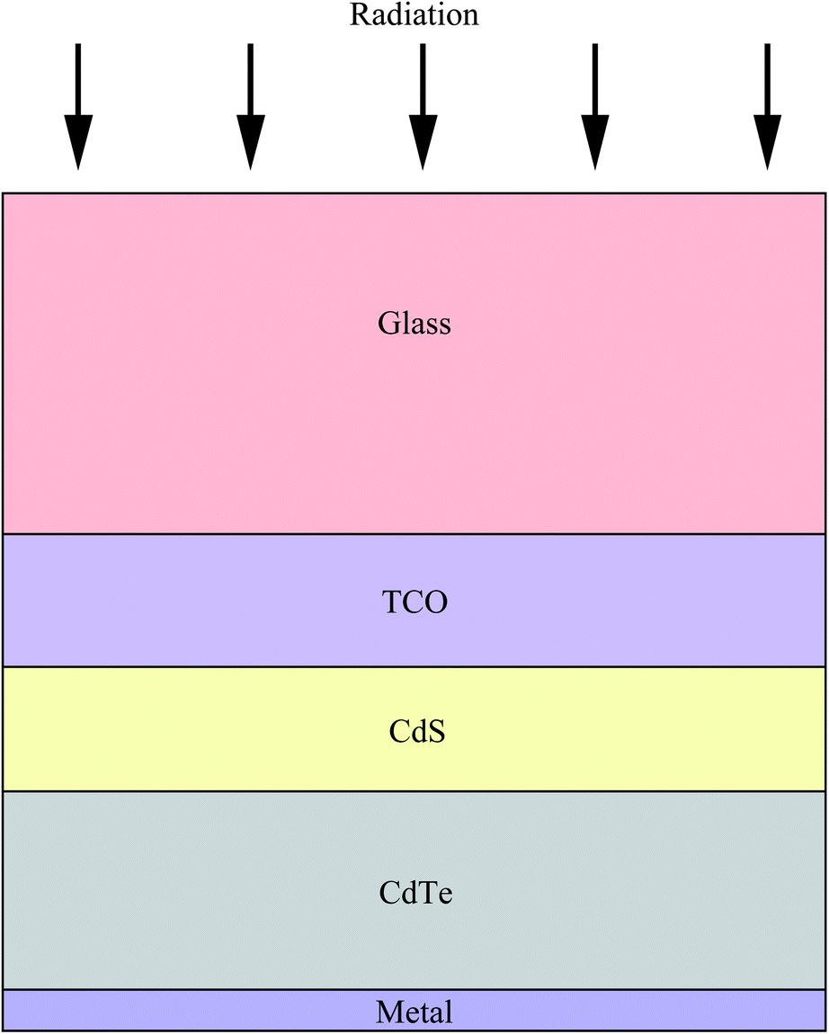 | ||
| Fig. 1 Schematic representation of a CdTe/CdS solar cell in the superstrate configuration. | ||
Both CdTe and CdS are quite stable and can be produced using various scalable techniques like CBD, CSS, MOCVD, ED, ALE, screen printing, sputtering, sintering, MBE and HVE.58–83 The conversion efficiency of the homojunction CdTe solar cell was not encouraging and hence a heterojunction with a wide band gap n-CdS semiconductor was developed. It is also reported that polycrystalline solar cells exhibit better performance compared to single crystal materials,84 which is probably due to the passivation of GBs by the segregation of materials like CdF2, CdSO3 and CdSO4 in a CdS film or CdTeO3 in a CdTe film.84 In particular, band bending that forms near CdTe GBs effectively separates photogenerated charge carrier pairs, while the GB core is an efficient transport of minority carriers.85 However, such comparison cannot be justified as processing conditions for optimizing single crystal and polycrystalline cells are extremely different. For a small area module (1 cm2), the PV conversion attained is 16.5%, while the efficiency is slightly lower (10.5%) for large area modules (1400 cm2), which are being developed for large scale production.86–89 Although this efficiency is achieved on a laboratory scale, CdTe/CdS thin film solar cells have already arrived to a stage comparable to more sophisticated single crystal silicon materials technology.57
Previously published reviews discuss the back contact strategy, junction activation step and technology related issues, besides focusing on other PV materials like amorphous, microcrystalline and polycrystalline silicon solar cells, CuInSe2, CuInS2, CuIn1−xGaxSe2, multi junctions etc.27–38,44–50,53 In this review, key issues in fundamental and critical aspects of CdTe/CdS PVs are discussed from the viewpoint of materials science encompassing their physics – device performance, and chemical concepts – and reactions occurring at various interfaces.
2. Choice of CdS and CdTe
As the solar cell efficiency depends on the product of Voc and Isc, there exists optimum band gap energy in a device for producing maximum output. A detailed analysis for the dependence of power conversion efficiency on the semiconductor band gap for the black body limit revealed that for terrestrial power generation under the AM 1.5 and AM 1 spectrum, the optimum band gap energy required is 1.5 eV which approximates to semiconductors like CdTe, InP, GaAs and CuInS2 (Fig. 2).90–94 In practice, a band gap energy in the range of 1.0–1.7 eV like mono crystalline and polycrystalline silicon (1.12 eV), CuInSe2 (1.05 eV) and α-Si:H (1.7 eV) also find applications. The silicon based devices are usually a homojunction, while most of the other devices constitute a heterojunction.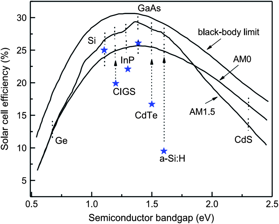 | ||
| Fig. 2 Power conversion efficiency as a function of semiconductor band gap. Asterisks show the best confirmed solar cell efficiencies under AM 1.5 illumination (reprinted with permission from ref. 92; copyright @ 2006 Elsevier). | ||
2.1 Properties of the CdTe absorber layer
The CdTe is a robust semiconducting material, which can be prepared by various synthetic routes in a highly reproducible manner and its remarkable tolerance towards high processing temperatures makes it ideal for large scale industrial production. The CdTe/CdS solar cells are unusual as they exhibit superior performance only in the superstrate configuration compared to their substrate counterparts. These two polycrystals (CdTe and CdS) are chemically stable and high optical quality layers are deposited in the temperature range of 400–600 °C. Since high thermal treatment is involved during CdTe deposition by most of the preparative techniques, CdTe films are associated with VCd giving rise to p-type conductivity. The high ionicity (72%) of CdTe results in well-passivated crystallites, while high chemical–thermal stability is associated with strong chemical bonding (5.75 eV).95 The stability region of CdTe is extremely narrow (2 × 10⁻⁶ atom% wide) and is symmetrical with a perfect stoichiometry at 400 °C.38 At a temperature of 500–600 °C (deposition of CdTe via CSS), p-CdTe will have a carrier concentration >1014 cm−3 that is sufficient to form a good junction with its n-type partner. This is of paramount importance, since doping of polycrystalline film must be avoided as foreign elements, especially metals, segregate into the GBs.57 The stability region of the Te-rich side increases to about 10−5 atom% close to the CdTe melting point (1090 °C). In vacuum, CdTe sublimates such that the vapor phase consists of Cd atoms and Te2 molecules in exact proportion to the solid (partial pressure of Cd = 2 × partial pressure of Te2). Consequently, CdTe deposition by thermal evaporation does not constitute any stoichiometric problems.38 The CdTe solar cells have proven to be extremely stable, and devices with notable efficiency >10% are fabricated by several deposition methods.CdTe is potentially a good absorber due to its large absorption coefficient (>1 × 104 cm−1)96,97 and its direct band gap allows only a few microns of material to absorb 90% of photons with Eg > 1.45 eV.2,57,94 Another important aspect is that the carrier lifetime for CdTe is small (of the order of 1 × 10⁻⁷ s or less) with a mobility ranging from 10 to 100 cm2 V−1 s−1. The short optical absorption length in II–VI compounds also renders the carrier diffusion length in minority carrier devices relatively insignificant. The diffusion length in CdTe film grains will be between 1 and 5 μm and hence the active layer thickness will be within the limits of 1–5 μm.27 Thus, solar cells can be fabricated using a much lesser quantity of CdTe with a depletion layer width comparable to film thickness. The reduced thickness of the absorber gives rise to a intense electric field and therefore a large fraction of carriers will be generated within the depletion layer, facilitating efficient carrier collection.4 CdTe offers flexibility in device design as it forms isostructural and isoelectronic alloys with other II–VI compounds such as HgTe and ZnTe, allowing the band gap of the absorber layer to be narrowed or widened for tandem cell and optical detector applications.98 CdTe has a high temperature coefficient of bandgap (2.3–5.4 × 10⁻⁴ eV K−1),38 the highest stability against electron/proton irradiation (Fig. 3), a low stacking-fault energy, is predisposed to twinning and planar faulting and exhibits both p-type and n-type conductivity.99,100 As grown CdTe under Cd-rich conditions is n-type due to the Fermi-level being pinned near the mid gap by the compensating donor effect Cdi2+. Under the Te-rich limit, CdTe behaves as p-type as the Fermi-level is pinned close to VBM.101
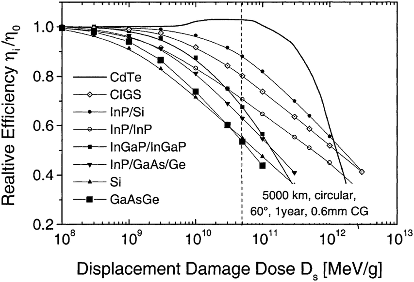 | ||
| Fig. 3 Degradation curves of different solar cells (reprinted with permission from ref. 116; copyright @ 2004 Elsevier). | ||
Since the band gaps of bulk CdTe and CdS are 1.5 and 2.4 eV respectively, photons with energies within this range can reach the CdTe layer, contributing to the cells photocurrent.102 The theoretical efficiency limit for cells with the CdTe room temperature band gap (1.5 eV) is 30%.103–105 However, a practical efficiency of 18.5% could be expected for this material with a Voc of 0.88 V and Jsc of 270 A m−2 (with a negligibly thin CdS).106 The maximum photocurrent available from a CdTe cell under the global spectrum normalized to 100 mW cm−2 is 30.5 mA cm−2.44 The efficiency of solar cells can be further enhanced by considering a few aspects like increasing the grain size of CdTe and using a thin absorber layer with controlled film morphology to achieve compact and pinhole-free layers so as to avoid short circuits, shunt resistance and weak diodes.
2.2 Properties of CdS window layer
The CdS is the most widely used window material for thin film CdTe solar cells. The multiple roles of CdS are: (i) it acts as a window layer relating to spectral response at shorter wavelength regions; (ii) it plays a vital role for the crystallinity of the CdTe layer; (iii) it facilitates the formation of large bandgap CdTe1−xSx mixed crystal layers near the CdS–CdTe interface, which improve the properties of the absorber layer. CdS is used either for establishing an electric field at the heterojunction interface that collects the photogenerated charge carriers or as “buffer layer” that avoids the interface mismatch between TCO and CdTe.27 If CdS is used as a “buffer layer”, its resistivity should be high enough to ensure stoichiometry and a good quality layer in order to reduce the trap-state density at the interface to improve junction properties. Alternatively, if CdS is used as the active layer of the heterojunction itself, resistivity must be small for a good ohmic contact with the TCO layer and the electric field at the CdS–CdTe interface should be high to improve the Voc.27 The n-CdS window layer is an essential component of the cell; although a p-CdTe/TCO junction with efficiency >10% has been reported,107 such a junction was however found to be inferior. The fundamental requirements of CdS are that it should be conductive (n ∼ 1016 cm−3) and thin enough to allow high transmission (50–100 nm), and uniform in order to suppress short circuit effects.The C–V calculation for CdTe/CdS solar cells indicated a ΔEv of 0.87 eV and an interface charge density (σ) of around 1 × 1013 cm−2, which are important parameters in the improvement of solar cell quality.108 Niles and Hocst experimentally reported a ΔEv of 0.65 eV by the photoemission method109 and Wei et al. reported a value of 0.99 eV using first-principles calculations.110 The stepwise deposition of a CdTe film on a wurtzite CdS {0001} single crystalline substrate by MBE resulted in a ΔEv of 0.65 eV and a ΔEc of 0.31 eV, indicating type-I band alignment (Fig. 4). Also, CdS showed strong upward band bending of 0.55 eV during junction formation.111 The reported band offset for the CdTe/CdS heterojunction falls into a wide range of 0.58–1.19 eV.109,112–114 Band offsets are quite sensitive to sample preparation conditions such as substrate orientation, surface/interface states and heterojunction formation sequence.
 | ||
| Fig. 4 Band alignments of CdS (0001)/CdTe heterojunction (reprinted with permission from ref. 111; copyright @ 2012 IOP Science). | ||
Due to the fascinating PV properties of the window/absorber layer and good scalability of techniques used to produce thin film PVs, these devices are already produced in modules of 60 × 120 cm2 by two companies: Antec Solar in Germany and First Solar in the United States.57 This heterostructure is usually preferred because the minority diffusion length of electrons in a p-type semiconductor is much greater than that of holes in an n-type semiconductor.115 These solar cells perform faster recovery from the induced damage, presumably due to strong defect compensation effects in CdTe.116 Recovery of light-stress induced degradation can be caused by either storage or annealing in the dark.117 In this case dissociation of acceptor defects in CdS, such as substitution of Cu at the Cd site (Cu1Cd) and a [VCd–Cui]1 complex into VCd and Cui, back-diffusion of Cu+ driven by a concentration gradient and a restored junction field leads to the recovery of the original behavior.117 Even the reflection losses for this device are not critical as compared to a silicon solar cell. The coefficient of reflection from the mirror surface of silicon is at least 30%, and higher than 50% in the region of λ < 400 nm.118 Thus, the better formation enthalpy, good chemical stability, favorable opto-electronic properties and unique interfacial structure of CdS–CdTe have driven this novel device architecture as a promising contender for solar cell applications.
3. Problems associated with CdTe/CdS solar cells
3.1 Technical and environmental issues
The performance of a heterojunction depends on the formation of an interface structure during thin film deposition and any subsequent processing. The variation in the quality of materials obtained by different techniques or even with same approach but under varied growth conditions can influence the device performance. Diverse preparation techniques can also cause variation in material properties such as carrier lifetime, mobility and their absorption coefficient. One of the important requisitions for this device is to reduce the thickness of the PV active layer from the standpoint of lowering production costs and cadmium toxicity. Another issue in CdTe technology is the junction activation step involving a toxic chlorine atmosphere which should be either modified or completely eliminated. Even if full recycling of modules is offered by manufacturers and designers, it is still doubtful that the production and deployment of cadmium-based modules could be so environmentally benign as to justify their use.119Tellurium is a scarce element; hence CdTe PV module production seems to be limited to a peak of a few gigawatts per year and constrained due to the volume of potentially hazardous cadmium compounds being used in a typically 3–8 μm thick CdTe layer.119,120 Therefore, it is necessary to reduce the CdTe thickness layer in these devices. The development of cells with a much thinner layer (<1 μm, ultrathin) would help to extend tellurium supplies with additional benefits like improved understanding of device operation, reduced cost of materials and manufacturing time, high throughput, easier cell isolation, minimum use of toxic materials and reduced secondary waste treatment cost at the manufacturing process.120 Although CdTe with a typical thickness of 1–2 μm would be optimal for both optical and electrical applications, in practice it is very hard to achieve without a subset of problems. The submicron absorber thickness deteriorates the device performance quickly due to increased defect densities accompanied by the loss of photocurrent. In addition, the absorber layer thickness becomes much smaller than the photon absorption length leading to incomplete optical absorption with a thin absorber (deep penetration loss).121,122
3.2 Factors responsible for device degradation
Depending on the processing conditions, sodium present in glass substrates diffuses into the active layer resulting in grain growth and GBs widen followed by the shunting of solar cells. Such changes also facilitate the high degree of interdiffusion between CdS and CdTe and favor the junction formation of CdTe or CdTe1−xSx with TCO.128 The space charge width, and hence cell parameters, decreased with increase in NaF thickness deposited on CdTe prior to the junction activation step (Table 1). The presence of sodium alters the surface energy of both CdS and CdTe and also modifies the GBs.128 Sodium serves as shallow acceptor in CdTe with a low activation energy of 59 meV (ref. 129) and increases acceptor density lowering the space charge width.130 In contrast, Sites and Pan reported an increase of Voc with sodium diffusion into the device structure.130 The sodium contamination from substrates can be reduced either by using expensive low alkaline borosilicate glass or by the inclusion of a diffusion barrier layer, which however results in increased production cost. By avoiding sodium contamination, excess interface intermixing and recrystallization as well as shunting paths can be prevented and the CdS thickness can be reduced without any adverse effects on the cell parameters. Since solar cells or modules are operated at higher temperature, diffusion of metal via VCd states and along tellurium-rich GBs through the absorber layer will be enhanced depending on characteristic diffusion velocity and diffusion mechanism of the metal.131,132 Even changing the stoichiometry of metal/back contact interface and lowering the contact area will facilitate the degradation. The impurities originating from front/back contact accumulate at the window layer near the space charge region and destabilize the device efficiency.
| NaF thickness/nm | V oc/mV | FF (%) | J sc/mA cm−2 | η (%) | R p/kΩ cm2 | SCR/μm | E g/eV |
|---|---|---|---|---|---|---|---|
| 0 | 818 | 72.5 | 23.8 | 14.0 | 4.5 | 2.4 | 1.454 |
| 0.75 | 784 | 64.5 | 24.5 | 12.4 | 2.6 | 1.6 | 1.450 |
| 1.5 | 740 | 53.3 | 23.7 | 9.4 | 0.8 | 0.9 | 1.449 |
| 3.0 | 629 | 40.0 | 21.1 | 5.3 | 0.3 | 0.8 | 1.449 |
| 6.0 | 494 | 38.8 | 15.0 | 2.7 | 0.2 | 0.5 | 1.466 |
| 12 | 508 | 42.1 | 12.8 | 2.6 | 0.2 | 0.3 | 1.468 |
The main structural defects in the polycrystalline films are GBs. The presence of GBs affects the semiconductor optical absorption, carrier mobility and lifetime.85 The crystal defects and impurities at GBs can induce deep level energy states within the band gap leading to trapped localized charges. These charges create a region depleted of majority charge carriers near the GB, causing an electrostatic potential barrier (band bending) for majority carrier transport with consequent reduction in effective mobility across the junction.133 Thus, the enhanced recombination of charge carriers via localized energy states will be detrimental to photocurrent collection.27,134,135 The diffusion of elements in solids can be realized by either direct diffusion (direct exchange with adjacent atom) or indirect diffusion (involving point defects). In general, indirect diffusion is favorable with the availability of vacancies in solid matrix. The impurity diffusion in polycrystalline CdTe proceeds via three channels – GBs, interstitial positions (i) and vacancies (v) inside grains. As a consequence, the diffusion of impurities must be characterized by means of three diffusion coefficients – along the GBs, interstitial and vacancies, which follows the order: DGBs > Di > Dv. Thus, the GBs with a high density of vacancies facilitate the rapid diffusion process.136 It is suggested that grain boundary diffusion is a very likely mechanism for the impurity transport into the device and dopant diffusion coefficient are enhanced at GBs.127,131 GBs in CdTe have downward bending, while those in CdTe1−xSx have upward bending.137 The decoration of GBs with tellurium inclusion reduces the band bending effect in CdTe. The boundaries between single crystal grains in polycrystalline CdTe is anticipated to have a strong impact upon the PV performance.138 It is expected that a high density of defects exists at GBs (e.g. dangling bonds, dislocations) and that impurities or stoichiometric excess tellurium will segregate to the boundary environment which may benefit the “gettering” of these defects from the grain bulk, improving the grain's crystalline quality.138,139 Thus, the role of GBs on device performance remains controversial. In any case, GBs give rise to a host of issues including: (i) enhanced migration of dopants;140 (ii) device shunting; (iii) high recombination velocities due to unpassivated surfaces; (iv) significant current leakage;135 (v) a barrier to current transport.134 The carrier generated at the vicinity of GBs will have much higher probability of recombination at the boundary compared to those generated closer to the junction.2 There are numerous surface/interfaces in the cell with sub-micrometer grain-size having a high concentration of GBs which act as internal interfaces.
The GBs create interdependencies between various parts of the device as they form an interconnected network within the thin film and couple critical components including the back contact, CdTe or CdS grains and various interfaces. These GBs are easily oxidized in the presence of oxygen, which occupies open spaces in the dislocation cores and VTe sites at GBs forming Cd–O bonds.141 Since the Cd–O bond length is smaller than the Cd–Te bond, sulfur diffusion along the GBs will be suppressed compared to the bulk. The sulfur diffusion depth inside the grains will be much shorter leading to a thinner CdTe1−xSx layer compared to the sample grown without the presence of oxygen (Fig. 5). Thus, the presence of sulfur at the back contact primarily arises from grain boundary diffusion.141 In II–VI compounds, GBs can be passivated partially by chemical treatment such as oxidation. The oxidized products like CdO usually exhibit n-type conductivity due to oxygen deficiencies and hence the surface p-absorber grains are converted to n-type conductivity. The carriers generated in the vicinity of the vertical p–n junction will be effectively collected at the junction, which are otherwise lost in recombination pathways.2
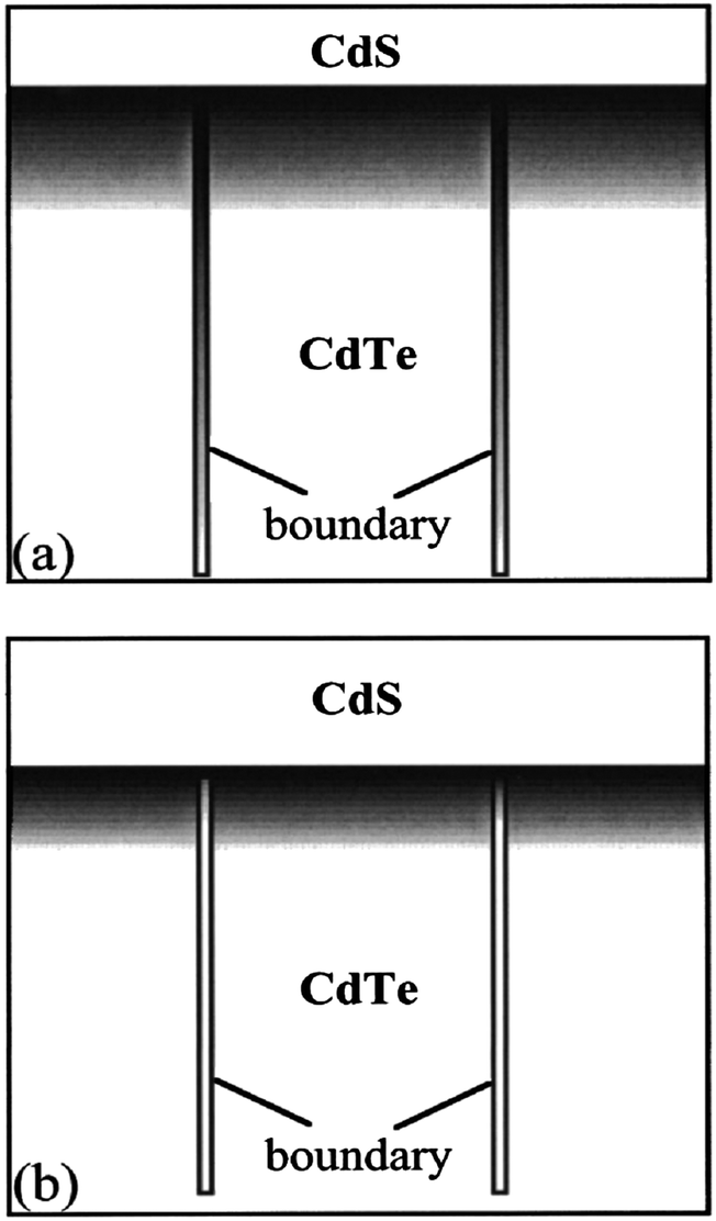 | ||
| Fig. 5 Modes for the sulfur profiles inside grains and along grain boundaries for the CdTe grown (a) without and (b) with the presence of O during growth. The gray scale indicates the relative sulfur concentration in the CdTe side (reprinted with permission from ref. 141; copyright @ 2001 American Institute of Physics). | ||
The passivation of GBs is important in the fabrication of high efficiency thin film CdTe/CdS solar cells. A more economical method for minimizing the diffusion of impurities is to reduce the substrate deposition temperature during device fabrication. The low temperature intrinsically reduces diffusion as the diffusion constant follows Arrhenius characteristics (exponential dependence with temperature).128 The stability depends on the spatial changes of defects and impurities from the source materials during the processing conditions. Such impurities can have strong and detrimental effects on the electronic properties of the device, which can be observed in voltage-dependent QE measurements that allow distinguishing effects in different cell layers, especially in CdS by means of spectral resolution.142,143 However, the magnitude of inhibitory effects by each specific impurity and its minimum acceptable concentration in device efficiency is not extensively investigated so far. Thus, grain size is an important parameter as it determines the grain boundary density and GBs are preferred diffusion pathways for impurity transport in polycrystalline materials. It is therefore important to minimize the impact of grain boundary effects by increasing the grain size for better performance.
3.3 Optical absorption losses
Though the CdTe/CdS solar cells have demonstrated the highest performance to date, the CdS window layer itself limits the maximum achievable efficiency. The CdTe/CdS heterostructure exhibits a very high spectral response in the wavelength region 500–850 nm with a sharp rise at 850 nm and remains insensitive below 500 nm. Due to its moderate band gap, CdS serves as a filter for high energy photons of the solar spectrum (<500 nm) resulting in absorption loss without contributing to net photocurrent generation. The CdS film thickness of 0.1 μm absorbs 63% of incident radiation with an energy greater than its band gap,146 while photocurrent loss can reach to an extent of 30.5 mA cm−2.147 Thus, generation of charge carriers by energetic photons in the n-CdS layer takes place at the surface far away from the depletion region resulting in a surface recombination current, and consequently reduces useful current delivered by the cell to the load.102 The efficiencies of solar cells can also be reduced by the optical loss at various interfaces. Before reaching the photoelectrically active CdTe layer, solar radiation must penetrate into the glass plate, TCO and CdS in the superstrate configuration (Fig. 1). Obviously, this is accompanied by optical losses upon reflection from the interfaces like air–glass, glass–TCO, TCO–CdS and CdS–CdTe and absorption in glass plate, TCO and CdS. The reflection loss at the interfaces results in lowering of the Isc by 9%, whereas absorption in TCO and CdS layers with a typical thickness leads to a loss of 15–16% and 22–24% for SnO2 and ITO front electrodes respectively. The reflections from the front surface of a glass without anti-reflective coating reduce the Isc by 3.5%.118 In addition, the integrated device current decreased from 22.02 to 18.32 mA cm−2 for a 100 nm thick CdS film, while such loss was less pronounced (22.55 to 20.44 mA cm−2) for an ultrathin CdS film.62 Thus, parasitic optical absorption in the CdS layer results in a predominant photocurrent loss making it necessary to minimize CdS film thickness (<100 nm) to ensure a maximum amount of light is absorbed by the CdTe layer. Maintaining the CdS thickness uniformity at the manufacturing scale requires control over the CdS deposition and CdS–CdTe interdiffusion during the fabrication of both the absorber and window layer. It is also difficult to obtain deposited CdS free from holes and caverns without empty spaces among the grains and with a homogeneous grain size distribution to favor nucleation and particle growth kinetics for CdTe.The absorption loss in CdS cannot be avoided by reducing the thickness alone since it is related to interband optical transitions. Even at a thickness of 50 nm, a decrease in the Isc caused by absorption in the CdS layer is 10% and further loss continued when the thickness was doubled.118 However, there is a trade-off between the current gain and voltage as well as FF losses with the reduction of CdS thickness. It is better to use a modified CdS layer with interdiffusion between a special sublayer and CdS or to replace CdS with another wide band-gap semiconductor to avoid optical losses. The non-radiative recombination at several interfaces also contributes to additional optical loss from the cell structure.148 Considering the portion of CdS reacting with CdTe to form intrinsic layer CdS1−xTex, demand for high quality CdS films acquires even more importance. The tendency to form a CdS1−yTey alloy, absorption in the lower wavelength region and the large lattice mismatch with CdTe provides room to develop an alternate window material that overcomes these problems.
3.4 Fabrication of back ohmic contact and associated drawbacks
(a) Chemical etching of CdTe surface. Surface pretreatments are commonly applied to modify the surface defect chemistry of the CdTe layer to facilitate low resistance contact formation.165–168 Surface chemical etching of CdTe with dilute HCl, Br2–CH3OH, K2Cr2O7–H2SO4, or a mixture of HNO3 and H3PO4 (NP) in water is made to produce a Te-rich layer, which effectively leads to a p+ doped layer resulting in a field at the back surface.145,158,169–171 Irrespective of chemical treatment, this etching process converts the near surface region of CdTe film from a stoichiometric to a Te-rich p-type conductive layer. The ΔEv will be small between the p-CdTe and Te layer (0.26 eV), which facilitates hole transfer from the p-CdTe into Te layer. Thus, band bending will occur at CdTe/Te interface and act as minority-carrier reflector to reduce recombination current on the back surface and at GBs, consequently increasing Voc. The CL measurements revealed that these etched layers either reduce the electron penetration depth or absorb photons emitted from the underlying CdTe. The K2Cr2O7–H2SO4 form an undesirable TeO2 layer that hinders low-resistance contact formation, while Br2–CH3OH treatment causes the penetration of bromine into the entire CdTe thin film and accumulates at the CdS–CdTe interface and front contact.158 The product CdBr2 is soluble in both methanol and water, which can be subsequently removed from the surface by agitating, rinsing and leaving behind the Te-rich CdTe. It is reported that a Br2/ethylene glycol etch (10 s) completely eliminates roll-over, while Br2/CH3OH only reduced the degree of roll-over even after long etching (30 s). This difference between etch solutions arose from the solvent viscosity, with ethylene glycol solution being a slower etchant due to its higher viscosity.117 Interestingly, NP etching is preferential to leaving the CdTe surface Te-rich thus increasing the surface conductivity and aiding the formation of tunneling junctions with more reliable contacts.172 Recently reported HNO3–CH3COOH (NA) etching also formed a tellurium layer of <1 nm, with the etching rate being slightly slow compared to NP etching due to the low H+ concentration released from CH3COOH.173 This chemical etching is necessary in order to remove any oxidized byproduct and residual CdCl2 from the CdTe film surface that is normally formed during the junction activation step.174
As an alternative to chemical etching processes, deposition of a Te layer on the top of CdTe is also studied. A post deposition annealing of Te–CdTe system produces a Te-rich p+ layer (band gap of Te layer is 0.33 eV) on the CdTe surface, which reduces the back contact barrier.175 Niles et al.176 reported that the minimization of the Schottky barrier close to 0.26 eV could be achieved for a thick Te layer that retains p-type conductivity. In contrast, a thinner Te layer will be dominated by interface states and will be n-type, leading to a higher barrier.176 Li et al.158 reported that preferential etching occurs along the GBs of CdTe even at low concentrations of NP, while more NP etching alters significantly the bulk properties of the thin film by exposing GBs and leaving behind a conductive Te-rich layer that forms shunting paths between the back contact and CdS or TCO layers, suppressing the device performance. The etching to produce a Te-rich surface is more effective in minimizing the Schottky barrier if the etching time is slightly prolonged. However, this process will be accompanied by the penetration of a metastable concentration of excess Te (VCd) into the subsurface region and can extend into the heterointerface; device shunting problems will be prevalent with overetching.
The Te-rich surface layers are susceptible to the formation of an oxidized product (TeO2), leading to contact degradation through the formation of a metal/insulator/semiconductor heterostructure.123,177–179 The etching time and etch concentration are inversely interdependent; for low etch time, high concentration of etch solution is preferred and vice versa. The use of etching although common on the laboratory scale, cannot be preferred at the manufacturing level. Etching can lead to voids resulting in shunt paths between the crystal grains, if a very thin film absorber layer is employed.180 These modified etch layers can be removed with KOH/CH3OH etch.158 Understanding the nature of CdTe surface prior to, during and after chemical etching process is of vital importance to the successful back contacting process. It is believed that surface orientation, etching process and annealing atmosphere play an important role in the oxidation of the CdTe surface.181 Though etching can remove surface residues, it still fails to remove the traces from GBs.182 The thickness of the film must be duly considered for the careful control of etch concentration and duration and it is essential to optimize device performance while maintaining the grain boundary integrity.
(b) Deposition with metal. The use of metals as ohmic contacts due to their low resistivity is not desirable because of their diffusing ability in different layers deteriorating the device performance. Ohmic contacts are generally formed by in-diffusion of constituents of contact materials, which results in high doping of semiconductors. As a consequence, the space charge layer associated with the barrier becomes very thin which could be tunneled by charge carriers.173 Many metals deposited onto CdTe show significant limitations in device performance due to reaction and formation of metal telluride and elemental cadmium that could be responsible for pinning the Fermi level in CdTe.183 The materials used to obtain ohmic contact in superstrate CdTe devices are graphite paste, Te/Au, Sb/Au, Ni, PbTe, SnTe, HgTe, ZnTe, Cu/Au, Cu/graphite, Cu doped ZnTe with metallization and Cu/Mo.184–196
The most commonly used metal to make a non-rectifying contact with CdTe is Cu. There are various methods to apply Cu at the CdTe back surface; evaporation of thin Cu films onto the CdTe surface; application of graphite paste containing Cu powder/Cu salts or Cu doped alloys; and dipping or spraying the Te-rich surface with Cu salt solutions. An annealing step is required to initiate chemical reaction between Cu and Te to form the desired Cu2−xTe phase and distribute Cu into the CdTe film.197 CuxTe/CdTe can also be prepared by the deposition of CuxTe alloy on the CdTe film.198 Varying the copper thickness during deposition probably alters both structural and optical properties of the CuxTe layer.
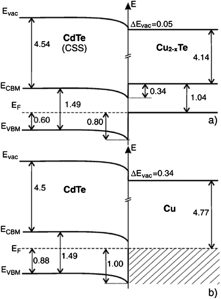 | ||
| Fig. 6 Band diagram for the (a) CdTe/Cu2−xTe and (b) CdTe/Cu interface as determined by photoelectron spectroscopy (reprinted with permission from ref. 206; copyright @ 2007 Elsevier). | ||
The Fermi energy on the CdS side is close to its CBM and it is close to the VBM on the CdTe side. Hence the formation energy of CuCd− could be lower in n-CdS than in p-CdTe, promoting Cu diffusion from the p-CdTe layer to the n-CdS layer.110 The driving force for Cu diffusion stems from the high affinity of Cu towards chemical bonding with the S of CdS compared to the Te of CdTe, due to the greater chemical stability of Cu–S over Cu–Te.117 This results in the formation of a p+-Cu2−δS phase at the CdS–CdTe interface209 and also forms ClS–CuCd complexes and CuCd centers at the expense of ClS–VCd complexes.117 The band gap of p+-Cu2−δS varies in the range of 1.0–2.3 eV depending on δ, which is typically smaller than the Eg of CdS thus reducing the electrically active photon flux into the absorber layer because of the additional absorption in p+-Cu2−δS leading to more optical losses.209 The Cu diffusion into CdS results in Cu depletion at the back contact, giving rise to the formation of a barrier for current transport. The Cu accumulation in CdS can be detrimental, only if carrier lifetimes in CdS will decrease below the value needed for electronic carrier transport across the film or if high enough to form a conducting Cu–Te shunting path through the device.124
In CdTe, Cu exists as an interstitial ion Cui+ giving rise to shallow donor states of 55 meV (ref. 210), or substituting for Cd atom to form deep acceptor states CuCd− with an activation energy in the range of 0.28–0.34 eV, attributed to its amphoteric behaviour.211–220 The Cu can also form neutral complexes (CuCd−–Cui+) in CdTe which contains only a small percentage of electrically active Cu atoms in the crystal lattice. Complexes with Cui+ and VCd (Cui+–VCd−) are relatively shallow acceptors that stabilize the isolated VCd− and other associated complexes.216–218 The Cu migration in single crystal CdTe and in other II–VI compounds is characterized by a fast (Cui+) and slow diffusion component (CuCd). Investigations have shown that the interstitial form of Cu is a fast diffuser with a diffusion coefficient as high as 10−12 cm2 s−1 at 300 °C.217,221,222 The CL studies revealed that CuCd and Cui+–VCd− complexes are relatively deep and shallow acceptors, respectively. Both of these states do not co-exist and their distributions are different from each other. The primary diffuser is represented by Cui+–VCd− complexes, since their distribution is progressively uniform and deeper into the CdTe films. The diffusion of these complexes was accompanied by the dissociation of other states with VCd. On the other hand, Cu incorporation in the form of CuCd was highly nonuniform and restricted to the back-contact interface. These results suggest that Cu diffusion is limited by Cu incorporation into VCd, whereas Cui+ migration and subsequent complex formation represents most of the electrically active Cu centers in CdTe films in high efficiency solar cells.223
The effective thermal diffusion and photodiffusion of Cu in CdTe films are 7.3 × 10⁻⁷![[thin space (1/6-em)]](https://www.rsc.org/images/entities/char_2009.gif) exp(−0.33/kT) and 4.7 × 10⁻⁸exp(−0.2/kT), respectively, as estimated from resistivity versus duration of thermal or photoannealing in the temperature range of 60–200 °C.224 The activation energy for Cu photodiffusion (0.20 eV) is less than thermal diffusion (0.33 eV), attributable to the increase of the fast-migrating interstitial flux of photodiffused copper.225−226 Photoinduced diffusion is detrimental for solar cells because incident light gives rise to an intense electric field which makes the ions mobile within the lattice at relatively low temperature.44 The application of an electric field strongly influences Cu electromigration and formation/dissociation of Cui+–VCd/CuCd states affecting the performance by modifying the doping profile and carrier concentration in the absorber layer.227 The device without Cu may have a different recombination mechanism, but junction recombination follows a Shockley–Read–Hall mechanism, with Cu having a diode factor of 2 suggesting strong midgap recombination.228 Thus, the high diffusivity of Cu in CdTe and the apparent instability of Cu2−xTe are responsible for changes in device performance and characteristics upon exposure to light.
exp(−0.33/kT) and 4.7 × 10⁻⁸exp(−0.2/kT), respectively, as estimated from resistivity versus duration of thermal or photoannealing in the temperature range of 60–200 °C.224 The activation energy for Cu photodiffusion (0.20 eV) is less than thermal diffusion (0.33 eV), attributable to the increase of the fast-migrating interstitial flux of photodiffused copper.225−226 Photoinduced diffusion is detrimental for solar cells because incident light gives rise to an intense electric field which makes the ions mobile within the lattice at relatively low temperature.44 The application of an electric field strongly influences Cu electromigration and formation/dissociation of Cui+–VCd/CuCd states affecting the performance by modifying the doping profile and carrier concentration in the absorber layer.227 The device without Cu may have a different recombination mechanism, but junction recombination follows a Shockley–Read–Hall mechanism, with Cu having a diode factor of 2 suggesting strong midgap recombination.228 Thus, the high diffusivity of Cu in CdTe and the apparent instability of Cu2−xTe are responsible for changes in device performance and characteristics upon exposure to light.
Metal (M = Cu or Ag) doped CdTe are susceptible for degradation after aging ascribed to instability of substitutional acceptor states (MCd) and formation of complexes (VCd–Mi and or MCd–Mi).229 The aging effect was found to accelerate with light soaking. It is possible that copper might accumulate close to CdS/CdTe junction and reduce the depletion layer width or by introducing shunting paths at GBs.230 The acceleration of cell degradation under illumination during stress is explained by the lowering of the electrostatic potential barrier for the diffusion of positively charged Cu ions crossing the cell junction and therefore enhanced accumulation in CdS,117 which was also supported by SIMS profiling and accelerated lifetime tests.116 The Cu (or Au) serves as an acceptor in CdS and creates a light modulating barrier in CdS CB, which decreases the effective donor concentration by serving as a recombination centre.116 For Au as back contact, Au diffusion in CdTe can be described by the Arrhenius expression D = 4.4 × 10⁻⁷exp(−0.54 eV)/kT with a relatively low activation energy (0.54 eV).136 The diffusion of Au into grains proceeds by the dissociative mechanism – the migrating impurity quickly moves by way of interstitial sites and settles in vacancies. The mechanism of Au diffusion in CdTe takes place in two ways: (i) by fast migration along the GBs; (ii) by relatively slow migration into grains which are characterized by low and high activation energies, respectively.231,232 Grain boundary diffusion and diffusion into the grain boundary region are observed for the low and high temperature regimes, respectively. The diffusion-doping of Au into CdTe was not influenced by grain size. The weak influence of Au diffusion on the structural properties of CdTe was due to dispersal of Au atoms preferentially on VCd owing to the covalent radius proximity of Au and Cd.136
Other stress-related changes include the partial conversion of Cu2−xTe to CuxTe with varied copper content that is responsible for the back contact and device degradation.233 The high diffusivity of copper was found to be assisted by grain boundaries as well as the polycrystalline nature of CdTe.208,217,230,234,235 In general, diffusion along GBs is more facile compared to bulk grains because surface bonds are weaker compared to the bulk due to incomplete coordination. It should be noted that diffusion doping of n-CdTe by Cu will be accompanied by an increase of resistivity, whereas Cu diffusion in p-CdTe lowers the resistivity.224 Experimental evidence showed that the non-shallow acceptor states defect complex [VCd–ClTe]0/− and Cu substitution at Cd sites [CuCd]0/− play critical roles in the p-doping of CdTe.236
The stability of solar cells was also influenced by the amount of Cu at the back contact. The cell was susceptible to degradation that tends to stabilize after an estimated time of 4 years for 3 nm Cu, while the cell with <0.5 nm Cu improved its performance slightly (Fig. 7).237 In addition to Cu and Au, contacts of the commonly used Ag can also diffuse rapidly towards the junction and contribute to device degradation.238 The degradation was severe under reverse bias compared to forward bias with Cu, while the efficiency of the device without copper increased marginally and remained constant under reverse bias.224 The larger degradation rate under reverse bias was related to the high electric field intensity applied to the heterojunction compared to forward bias testing. Therefore, excess Cu should be avoided in the back contact to obtain long-term device stability.239 The diffusion of Cu into the cell structure depends on the junction internal field, which in turn relies on the fact that cell is driven either by an external bias or illumination by one or more suns. Fisher et al.117 reported that the cell (in)stability observed with thermal stress in air or humid conditions cannot always be associated with Cu diffusion or Cu doping into the cell structure. Instead, it was due to the action of atmospheric components on the back-contact interface and/or main cell junction.
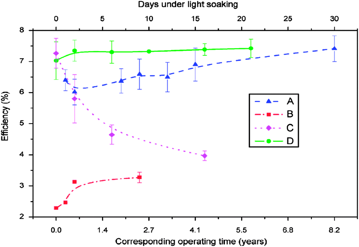 | ||
| Fig. 7 Accelerated lifetime stability tests of ITO/CdTe/CdS/FTO solar cell: before (A) and after annealing at 350 °C (B) and of ITO/Cu/CdTe/CdS/FTO solar cells with 3 nm copper deposition (C) and less than 0.5 nm copper deposition (D) (reprinted with permission from ref. 237; copyright @ 2007 Elsevier). | ||
In general, high performance CdTe solar cells requiring the formation of a low-resistance contact and increased efficiency can be achieved by incorporating an optimal amount of Cu at the back contact.240 A copper-containing back contact requires delicate control of the Cu content, as Cu deficiency leads to non-ohmic behavior, while excess Cu will affect the junction and can cause electrical shunts due to fast diffusion and deep penetration of Cu into the CdTe matrix.241 A full understanding of the role of Cu and other possible contact metals for back contact chemistry and their behavior within the device structure is required before optimizing the device performance.
The CdTe film surface evolves from crystalline to a low-melting glassy mixture of oxides and tellurides with heat treatment in the range of 300–550 °C.243 The elemental tellurium might arise from the decomposition of CdTe having a higher melting point than the annealed temperature of 450–550 °C, at which slurry mixtures of CdTe and oxides were observed. Such oxidized products were not observed at 450 °C, but prevailed in the samples calcined at 550 °C.243 The growth of insulating CdTeO3 between a back electrode and the CdTe surface deforms the I–V characteristics and declines the lifetime of solar cell.244 It is often assumed that the oxide does not form a barrier to charge carrier as it is thin enough to allow tunneling. However, thermionic emission current is affected if the barrier thickness exceeds 20 Å245 because electrons are blocked at the CdTe–oxide interface completely and recombine at the interface states.246 The oxidation process can affect the near-surface chemical equilibrium by removing disproportionate amounts of Cd or Te from the lattice, which complicates the defect vacancy structure in the film. Thus, careful control of oxygen and humidity in the annealing atmosphere is required to avoid the formation of unwanted oxides, which affects the VCd concentration within the CdTe film, resulting in poor device performance. CdTeO3 is the stable thermal oxide of CdTe, which decreases the hole current for the p-CdTe–oxide–metal junction due to the lower tunneling probability with increasing oxide thickness and increase in contact barrier height.247 These surface oxide residues are spatially discrete, located along the GBs and can penetrate deep below the CdTe surface affecting the junction activation step.242,248
The back contact is considered as a most important source of impurities diffusing into CdTe, CdS and the p–n junction that are responsible for device instability. An improved back contact is required to eliminate micro non-uniformities in the photocurrent response. Long term stability of the back contact may be achieved by using materials that are in thermodynamic equilibrium with CdTe and their metallization. In practice, true ohmic contacts are hard to realize and hence one defines a quasi-ohmic contact, exhibiting a low voltage drop across the metal–semiconductor interfaces, as compared to device voltage drop that may not necessarily be linear with current. The quasi-ohmic contact can be realized via convenient band bending at the metal–semiconductor junction.249
3.5 Interdiffusion between CdTe and CdS
During the fabrication and subsequent annealing, interfacial layers are formed via simultaneous interdiffusion of sulfur into CdTe and Te into CdS.255–257 This interdiffusion was qualitatively in line with the pseudo-binary CdTe–CdS phase diagram but the solubility limits were determined more accurately to be x = 0.03 and y = 0.06 at 415 °C.258 The formation of the CdSxTe1−x layer at the interface results in ‘x’ not exceeding 0.06 which represents an equilibrium solubility limit for sulfur in CdTe, although a layer of higher sulfur content might grow under non-equilibrium conditions.259,260 It is frequently surmised that the sulfur diffusion will prevail due to its smaller atomic radius compared to tellurium, which passivates electrically active GBs and relaxes lattice mismatch between CdTe and CdS to improve device performance.189,261,262 It is also reported that tellurium alloying with CdS can reduce the Isc of the device.62 However, the degree of sulfur diffusion to passivate defects still remains unclear. Based on near-field scanning optical microscopy, it was concluded that the sulfur composition in CdTe1−xSx was non-uniform due to grain boundary assisted diffusion, and sulfur diffuses preferentially along the GBs than in grain bulk. In fact, the grain boundary chemical composition will be rich in sulfur (5.8 atom%) compared to the maximum of 2 atom% found in the grain bulk.141,263–265 The amount of sulfur penetrating the bulk of CdTe from the grain boundary must be dictated by the bulk diffusion coefficient of sulfur in CdTe, transport of sulfur through the CdS layer, amount of sulfur available in CdS film and recrystallisation of the CdS layer.266–268 The extent of CdS consumption establishes a lower limit to thickness of CdS that can be employed while retaining a discrete CdS coating on TCO. Control over the effective CdS thickness obtained after processing is thus critical in achieving high current densities while maintaining the junction properties which govern the Voc. As discussed earlier, consumption of the CdS layer results in the formation of a CdTe1−xSx/TCO junction with inferior performance. Extensive alloying forms a non-uniform CdTe1−xSx layer consuming a significant quantity of CdS from the device and the excess interdiffusion may also lead to the dissolution of the heterojunction itself.137,269
The phase composition and thickness of the interfacial layer in the p–i–n structure depends on preparative conditions like substrate temperature, deposition time and annealing atmosphere, and this interfacial layer plays a decisive role in charge transfer. The CdTe layer can be separated into two groups depending on growth conditions; CdTe grown by CSS or CSVT with a deposition temperature above 500 °C are classified as a high temperature process, while techniques such as ED, HVE and sputtering which operate below 450 °C are low temperature processes. In the latter case, CdTe grows epitaxially on CdS with {111} of CdTe being parallel to the CdS {0001} plane.101 The CdS grain size is conserved across the interface and determines the grain diameter of CdTe, which remains unchanged throughout the absorber layer. The high density of microtwinning on the {111} plane is usually observed as a result of low stacking fault energy in CdTe.101 In contrast, CdTe growth at higher temperature will have a similar grain size compared to CdS at the interface and develops into much larger grains of several micrometers in diameter towards the CdTe top surface. The density of microtwins is smaller compared with low temperature grown CdTe and the orientational relationship between CdTe and CdS is less pronounced.101 The interdiffusion also depends on the growth technique. Electrodeposited films are grown at much lower temperature and the CdTe GBs are expected to be free from sulfur until the junction activation step or post deposition annealing. In addition, sulfur diffusion into the CdTe bulk takes a longer time compared to film growth itself. In contrast, sulfur diffusion along GBs will occur at a much faster rate than the film growth in the CSS technique, leading to thin coating of CdTe1−xSx that extends through the complete thickness of the CdTe film (Fig. 8).270 The compositional distribution of CdTe1−xSx is independent of CdTe thickness and rapid diffusion takes place near the CdS–CdTe interface.269
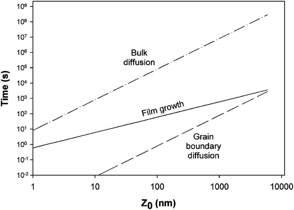 | ||
| Fig. 8 Comparison of rate of bulk and grain boundary diffusion with film growth rate, (5 μm film-Z0 grown in 5 min at 500 °C) (reprinted with permission from ref. 270; copyright @ 2003 Elsevier). | ||
The interatomic distance in the {111} plane of CdTe is 10% larger compared to the ‘c’ plane of CdS.271 It is relatively easy for the ‘c’ plane of the wurtzite structure and the {111} plane of the zinc blende structure to form the heterojunction, hence the preferred quasi-epitaxial growth habit of CdTe on CdS is CdTe {111}//CdS {0001}.126,272 The polarity of the {0002} layers of CdS is transferred across the interface to the {111} plane of the CdTe layer.126 It is evident that chemical bonding of Te at the CdS–CdTe interface is entirely different from that in bulk CdTe. The CdTe grown on CdS {0001} proceeds in a {111} direction at a higher rate compared to {10![[1 with combining macron]](https://www.rsc.org/images/entities/char_0031_0304.gif) 0} where the directional growth is {110}.251 The nucleation kinetics of CdTe at elevated temperature are faster on the {0001} plane, which is attributed to adhesion of Te forming a stable surface termination on CdS {0001} but not on {100}. This leads to a preferred {111} orientation of CdTe films deposited on the polycrystalline CdS substrate.251 The lattice mismatch is large enough to generate structural defects such as intrinsic stacking faults and misfit dislocations at the interface during CdTe film growth. This introduces interface states (1014 cm−2) at the junction,273,274 due to the smooth transition of CdS to CdTe through a mixed compound CdS1−xTex, with x varying between 0 and 1.274 Unfortunately, this type of heterojunction possess limited efficiency as this transition occurs through many atomic layers, which inevitably affects the Voc and FF. The transition must be sufficiently long to diminish interfacial states but need to be short to achieve high electric field.275 The isovalent substitution of sulfur for Te in CdTe/CdS heterojunction can reduce the strain arising from lattice mismatch and cause a reduction of interface states without introducing a defect state within the band gap. Meanwhile, an interstitial sulfur atom in the heterojunction will reduce lattice mismatch between the interface layers and create occupied electronic states at the upper CB.276 Based on DFT studies, it was concluded that an interstitial sulfur atom may induce the inversion of the surface Cd atoms and sublayer Te atoms of the Cd-terminated surface, while sulfur atoms adsorbed at top sites substitute for Te atoms or accumulate at the voids inside the Te-terminated CdTe surface as Si or Si1, acting as donors and then becoming impurities during grain growth.276 It is postulated that grain boundary passivation is partly caused by enrichment of GBs in CdTe with CdTe1−xSx and partly by Te enrichment that occurs during processing.137
0} where the directional growth is {110}.251 The nucleation kinetics of CdTe at elevated temperature are faster on the {0001} plane, which is attributed to adhesion of Te forming a stable surface termination on CdS {0001} but not on {100}. This leads to a preferred {111} orientation of CdTe films deposited on the polycrystalline CdS substrate.251 The lattice mismatch is large enough to generate structural defects such as intrinsic stacking faults and misfit dislocations at the interface during CdTe film growth. This introduces interface states (1014 cm−2) at the junction,273,274 due to the smooth transition of CdS to CdTe through a mixed compound CdS1−xTex, with x varying between 0 and 1.274 Unfortunately, this type of heterojunction possess limited efficiency as this transition occurs through many atomic layers, which inevitably affects the Voc and FF. The transition must be sufficiently long to diminish interfacial states but need to be short to achieve high electric field.275 The isovalent substitution of sulfur for Te in CdTe/CdS heterojunction can reduce the strain arising from lattice mismatch and cause a reduction of interface states without introducing a defect state within the band gap. Meanwhile, an interstitial sulfur atom in the heterojunction will reduce lattice mismatch between the interface layers and create occupied electronic states at the upper CB.276 Based on DFT studies, it was concluded that an interstitial sulfur atom may induce the inversion of the surface Cd atoms and sublayer Te atoms of the Cd-terminated surface, while sulfur atoms adsorbed at top sites substitute for Te atoms or accumulate at the voids inside the Te-terminated CdTe surface as Si or Si1, acting as donors and then becoming impurities during grain growth.276 It is postulated that grain boundary passivation is partly caused by enrichment of GBs in CdTe with CdTe1−xSx and partly by Te enrichment that occurs during processing.137
Ohata et al.277 have shown that intermixing of CdS and CdTe forms a bicrystal phase for CdTe1−xSx (0 < x < 1). The mixed phase has a zinc blende structure for x < 0.2 and a wurtzite structure for x > 0.2 at 700 °C, with a mixture of zinc blende and wurtzite phases between these values and phase transition from zinc blende to wurtzite was observed for x = 0.25 at 1000 °C (Fig. 9).260,277 In screen printed CdSxTe1−x films, a single phase (either zinc blende or wurtzite) was observed for 0 ≤ x ≤ 0.12 and 0.97 ≤ x ≤ 1, while a mixed phase was found for 0.68 ≤ x ≤ 0.97. Irrespective of the initial composition of CdTe and CdS, only CdS0.12Te0.88 and CdS0.95Te0.05 are formed.278 In general, stable crystallographic forms of interfacial alloys are the zinc blende structure (F43m) for Te-rich CdTe1−xSx, and the wurtzite (P63mc) for sulfur rich CdS1−yTey, which is in agreement with the CdS–CdTe phase diagram.279,280 Within these monophasic regions, Vegard's law was followed as reported by other research groups.259,281 Based on C–V characteristics at frequencies of 10 and 465 kHz, it was proposed that two types of CdTe1−xSx with a thickness of 2 × 10⁻³ (for x = 0.21) and 0.54 μm (for x = 0.68) are present with n-type and p-type conductivity, respectively.254
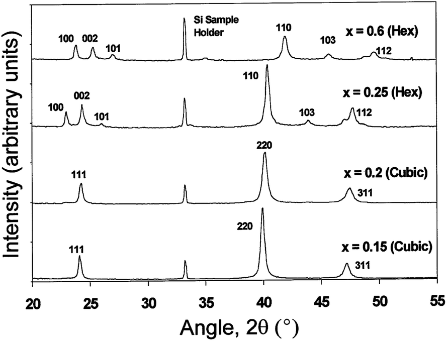 | ||
| Fig. 9 XRD spectra for CdSxTe1−x annealed at 1000 °C, with different compositions of ‘x’ varied from 0.15 to 0.6 (reprinted with permission from ref. 260; copyright @ 1999 Elsevier). | ||
The sulfur diffusion into CdTe is structurally rather than thermodynamically limited within the interface. Rogers et al.99 suggested that sulfur diffusion into CdTe occurs in a region delimited by a change in CdTe microstructure, which was apparent in as-deposited cells. Thus, control of sulfur diffusion and intermixing may be achieved through CdTe deposition parameters rather than post deposition thermodynamic treatment. As-deposited CdTe had an in-plane stress of +140 MPa and hence the defect formation is highly probable. The lattice parameter showed a gradual but significant increase from a depth of 1.3 μm below the surface to the CdS–CdTe interface (Fig. 10). Upon calcination, the lattice parameter decreased towards the interface. Thus, in-plane stress is tensile rather than compressive in the case of the as-deposited cell. Such a change in lattice parameter behavior may be reasonably attributed to sulfur diffusion from CdS into CdTe, which is otherwise negligible before calcination.99 The interdiffusion at the interface was maximized under the conditions of excess Te, which may be responsible for the displacement of the electrical p–n junction away from the metallurgical interface and into CdTe.282 The sulfur diffusion in the temperature range of 372–675 °C is governed by two mechanisms with activation energies of 1.06 (±0.04) and 1.7 (±0.2) eV.260 Though the nature of diffusion mechanism remains unclear, it was attributed to interstitial and substitutional sulfur diffusion with diffusivities in the range of 1.5 × 10⁻¹⁶ to 7 × 10⁻¹⁴ and 1.4 × 10⁻¹⁷ to 7 × 10⁻¹³ cm2 s−1, respectively. In another report, it was observed that the sulfur diffusion into CdTe was insignificant at 397 °C for 30 min annealing, while CdCl2 anneal (387 °C) revealed substantial diffusion with diffusivity D = 3.2 × 10⁻⁵exp(−1.2 eV)/kT cm2 s−1.283 Based on Auger electron spectroscopy, sulfur volume diffusion into CdTe was reported to be 4.39 × 10⁻¹⁵, 6.84 × 10⁻¹⁵ and 9.13 × 10⁻¹⁵ cm2 s−1 at a temperature of 250, 350 and 400 °C, respectively, with an effective diffusion coefficient of 1.02 × 10⁻¹³ cm2 s−1 and Ea of 0.142 eV.284 This activation energy is approximately equal to migration of VCd into CdTe (155 meV), indicating that sulfur diffusion at the CdS–CdTe interface is limited by VCd migration into the CdTe lattice. The diffusion profile did not indicate any signature of sulfur diffusion along the GBs in this study.284 In the presence of oxygen, both grain boundary and bulk diffusion of sulfur into CdTe will be approximately similar, while grain boundary diffusion predominates in the complete absence of oxygen.62
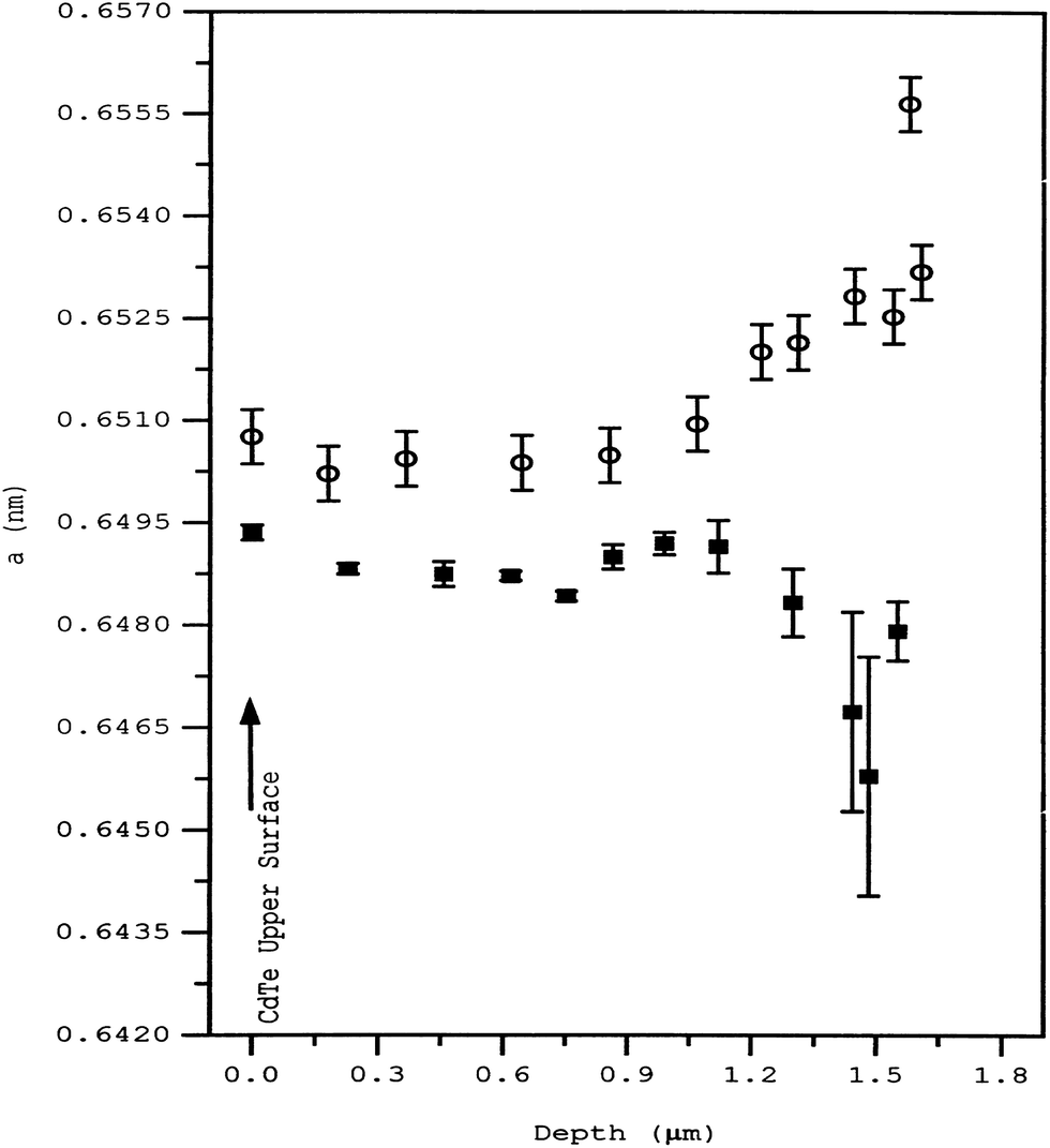 | ||
| Fig. 10 Lattice parameter ‘a’ for CdTe measured with depth for the as-deposited (○) and annealed (■) samples (reprinted with permission from ref. 99; copyright @ 1999 Elsevier). | ||
The CdS–CdTe interface is believed to be both a beneficial and limiting factor for solar cell performance, and the growth of the discrete region of intermediate composition during calcination can account for such behaviour. The diffusion process depends on annealing temperature, time, distribution of grains and defect density of the material. The quantification of inter-diffusion between window and absorber layer during the post deposition treatment is important in optimizing the annealing process and understanding device operation. The change in the doping level due to intermixing leads to a change in junction mechanism and space charge width, possibly resulting in reduced efficiency. It was suggested that the rapid sulfur diffusion into CdTe via GBs may cause increased shunting due to reduced band gap, or the formation of a metallurgical alloy in the intermixed region destabilizing the cell efficiency.241 The similar grain size between CdS and CdTe can favor efficient intermixing and decrease of interface defects. The important quantities are the energetic and spatial distribution of interface state density and defects as well as the alignment of energy bands and contact potential distribution. While the intrinsic interface states due to lattice mismatch and thermal expansion coefficient cannot be minimized, extrinsic interface states may be eliminated by optimizing the processing conditions.
The increase of sulfur content increases the band gap of the ternary compound except for the sulfur concentration below 25%, where the band gap decreases due to the bowing effect, leading to a decrease in the low-energy cut off of the device relative to pure CdTe.279,288 The bowing effect depressed the band gap of the ternary compound by 0.1 eV lower than the band gap of CdTe with the addition of 30% CdS.150 The bowing coefficient depends strongly on x. The large bowing coefficient for Cd (S, Te) alloy is attributed to a large lattice mismatch between CdTe and CdS and large differences in the s and p atomic eigenvalues of 1.93 and 1.00 eV, respectively, between sulfur and tellurium.110 The bowing coefficient is larger than the band gap difference of the constituents, indicating the addition of sulfur into CdTe initially reducing the band gap and increasing it thereafter. The total photoresponse remains, however, small because of the low photosensitivity of the solar cell in the spectral domain hν > Eg. The optical band gap follows the relationship:
| Eg(x) = 1.74x2 − 1.01x + 1.51. | (1) |
The composition of a solid solution (x) can be determined from its lattice parameter ‘a’, which is intermediate between those of CdS (a = 5.832 Å) and CdTe (a = 6.423 Å) using Vegard's law, assuming Eg is a linear function of ‘a’.285 The sulfur content ‘x’ of an CdTe1−xSx film was quantitatively determined from the lattice parameter by assuming Vegard's relationship: x = 1.508(6.481 − a), with ‘a’ being the lattice parameter of the sample.269 Optical measurements also supported the formation of ternary alloys that reduced the photoresponse at shorter wavelength and slightly extended response at longer wavelength.289–293 These regions are separated by a miscibility gap where both phases exist and optical absorption results from both wurtzite and zinc blende phases.279 This has been explained by the parabolic dependence of the CdSxTe1−x band gap upon stoichiometry.277
The interdiffusion between CdS and CdTe was evidenced from PL studies, which exhibit different features depending on the CdTe thickness; for 1.5 μm CdTe, PL spectra showed a deeper shift compared to a device with 1.0 μm CdTe (Fig. 11). Furthermore, the PL spectrum for 1.5 μm CdTe showed a broad and asymmetric peak at 2.019 eV (yellow band) and 1.825 eV (red band), while the 1 μm CdTe cell shows a broad peak in the yellow band. This was due to alloying as a result of interdiffusion, which causes the appearance of new peaks in the PL spectra.294 Duffy et al.295 reported the loss of photoactivity in CdS only for thick CdTe films, whereas CdS was still photoactive when thin layers of CdTe on CdS were annealed. This indicates that interdiffusion does not occur to the same extent in the case of CdTe thin layers on CdS. It follows that the space charge layer extends into the underlying CdS layer in the case of thinner CdTe films, which was not observed for thicker CdTe films. The CdTe1−xSx appears to be compositionally homogeneous in the junction region, whereas CdS1−yTey is highly defective and compositionally inhomogeneous. This accounts for photo-inactivity of CdS after heat treatment and junction formation. According to theoretical analysis, if the surface recombination rate at a CdS1−yTey/CdTe1−xSx heterojunction is <104 cm s−1, the device efficiency can be improved by moving the p–n junction towards the CdS1−yTey/CdTe1−xSx surface. Alternatively, shifting the p–n junction towards the CdTe region would be more preferable for a surface recombination rate of >104 cm s−1, such that it limits the negative role of surface recombination.296 For a low value of applied voltage, the space charge region is near to metallurgical junction where CdTe1−xSx is formed, while the space charge region is completely formed in CdTe at higher value of applied voltage (>0.4 V).108 In addition, capacitance–voltage and current–voltage characteristics also showed that CdS1−xTex formed at heterojunction are inhomogeneous in both conductivity and composition. The current–voltage characteristic in the current density range of 10−8 to 10−5 A cm−2 are governed by the thermal electron emission whereas current in the range of 10−4 to 10−2 A cm−2 is limited by recombination of charge carriers in the electroneutral region of the CdTe1−xSx solid solution.254
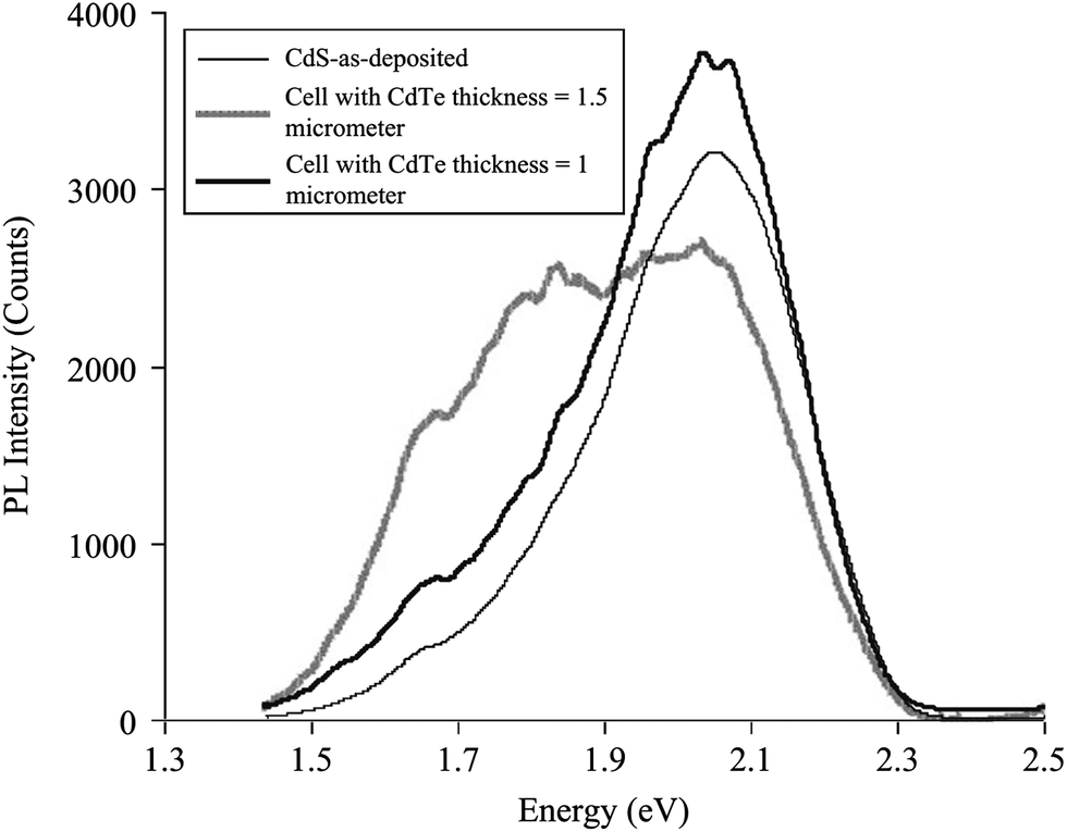 | ||
| Fig. 11 PL spectra of CdTe/CdS interface recorded at T = 60 K from the glass side using an Ar ion laser of wavelength 488 nm as excitation source (reprinted with permission from ref. 294; copyright @ 2012 Elsevier). | ||
From standpoint of band structure, it would be favorable if the VB of two materials did not include any relative offset that causes an energy spike at the junction. Also, there should be an appreciable built-in voltage at the junction, which can be transformed into useful work under the operating conditions. In addition, proper alignment of energy levels across the phase boundaries must be assured. The band edge alignments are decisive factors and are also objects of interface engineering which need to be optimized with respect to the electronic properties of dissimilar phase boundaries.297 The investigation of heterojunction band discontinuity is important because ΔEv and ΔEc determine the transport and confinement properties at the heterojunction.298−300 Thus, a major challenge is to find a proper alignment of energy bands across the interfaces of the heterostructure.
The combination of lattice mismatched or dissimilar materials cause Fermi level pinning or surface recombination losses, limiting the practical efficiency. Also, important are various interfaces between different layers, as each layer has a different crystallographic structure, morphology, particle size distribution, lattice constant, electron affinity/work function, thermal expansion coefficient, diffusion coefficient, chemical affinity, charge carrier mobility, mechanical adhesion etc. These interfaces results in stress/strain, defect/impurity states, surface/interface/bulk recombination centers, photon reflection/transmission/scattering, impurity diffusion and interdiffusion among the layers, changes in chemical composition and opto-electronic properties influencing the device performance.301 The interface properties are modified during device processing as a result of a growth process involving the sequential deposition of multilayers at different deposition conditions. In addition, post deposition involving high temperature annealing in different ambients can also alter interface and intergrain properties. Due to synergy of such complexity, the analysis of device parameters is complicated significantly.
Despite extensive research, composition of the interfacial layer between CdTe and CdS has not yet been fully understood and determined. A resolution of this problem would make it possible to fabricate new devices and enhance the performance of already existing CdTe/CdS devices. A full-scale understanding of the complex parameters controlling heterojunction formation with respect to deposition technique would allow insights into the interfacial electronic band structures and provide valuable information for analyzing device performance and failures at each consecutive stage.
4. Junction activation process: treatment methods and related effects
The photoelectric current in solar cells is influenced by the energetic spectrum of localized states within the band gap. The energetic diagram and physical characteristics of localized levels are determined by the annealing conditions. In order to obtain large grains as well as to improve the device electronic parameters, post-annealing of deposited films is a routine procedure in the device fabrication process. Most of the techniques rely on optimizing the properties of CdTe layer and the CdS–CdTe interface after their deposition with CdCl2 treatment, commonly referred to as a “junction activation process”.4.1 Wet and dry CdCl2 treatment
Irrespective of CdTe layer deposition method, CdCl2 activation step is standard and vital process in fabricating high efficiency PV devices. During this process, a small amount of solid CdCl2 may segregate on CdTe surface.302 The most commonly used agent is the hygroscopic salt CdCl2, which melts at 569 °C and boils at 963 °C with a vapor pressure of 13.3 kPa at 656 °C.197,303 The CdTe–CdCl2 phase diagram indicates only sub-atomic percentage solubility of Cl in CdTe at temperature below 525 °C and hence promotes Cl diffusion into the CdTe layer along GBs.263,304 The CdCl2 treatment by wet method involves: (i) dipping of CdTe layer in a CdCl2–CH3OH or CdCl2–H2O solution followed by drying to precipitate the CdCl2 film;305 (ii) the CdCl2 layer is deposited on CdTe followed by annealing. Conventionally activation treatment is performed by immersing a thin film in a CdCl2 solution and heated in air or inert atmosphere at 400–500 °C for a desired interval of time.275 After heat treatment, the sample is washed with water to remove residual CdCl2.The presence of oxygen during CdCl2 treatment results in a low resistance CdTe layer compared to the film prepared in a pure Ar atmosphere, typically with a carrier density in the order of 1014 to 1015 cm−3.44 The annealing in either He–O2 or in pure He leads to the formation of a surface chlorine residue comprising Cd, Te, Cl and O in the form of oxides and oxychlorides. The XPS analysis revealed that annealing in an inert atmosphere leads to the formation of Cl–Te bonds in the form of tellurium oxychlorides, while thermal treatment in oxidizing ambient results in Cd–O in the form of cadmium oxide along with tellurium oxychloride, which needs to be removed prior to back contact formation.306 It was shown that a solar cell comprising CSS-CdTe heat-treated with CdCl2 in an He atmosphere had a very similar cell performance compared to those treated in oxygen. This suggests that either the presence of oxygen did not affect the electronic defects, or the concentration of any oxygen-related complexes may be too low for detection using DLTS.307 In another study, DLTS studies revealed two closely spaced defects (0.44 & 0.42 eV below the CB) for air-activated solar cells and a broad band (although not characterized fully, it is located 0.40 eV below CB) for vacuum activated solar cells.308 The annealing of CdCl2 and CdTe in vacuum does not instigate any chemical reaction.306 In addition, Cl2 enhances the concentration of Cl2Te, which is a donor in CdTe and forms an n-type CdTe (S,O) layer at the interface under ambient oxygen.309
Dutta and Krishna310 suggested that in situ CdCl2 treatment results in less surface oxidation compared to an ex situ process, as the latter promotes Te oxidation on the surface and the former gives a relatively oxide-free surface. This means that in situ treatment can provide a chemically clean surface for efficient back contact formation.311 However, in situ CdCl2 treatment was effective only at the surface and up to p-type doping, which is restricted to a few layers of CdTe film only.312 The advantage of wet CdCl2 treatment lies in the handling and easy disposal of the rinsate. However, this surface treatment is effective only for small-cell fabrication and fails for large area manufacturing due to a non-uniform distribution of CdCl2 and processing in a humid environment leading to cell degradation. In addition, residual CdCl2 may not be eliminated completely by washing, as the formation of water-insoluble oxychlorides can stick to the film.306 As an alternative to the wet method, vapor treatment of CdTe with chloride vapor has been reported to yield better reproducibility and is beneficial for process control as it eliminates the formation of liquid waste associated with the solution method.313–318 The processing time is reduced since simultaneous deposition and heat treatment is involved, and it eliminates cadmium-containing waste accompanied by the ease of integration in an inline vacuum manufacturing process.147
In any case, CdCl2 is believed to act as a fluxing agent that increases the atomic mobility of CdTe or CdS at the annealing temperature. Increasing the temperature above 500 °C, the grain size becomes smaller and pinholes exist causing short or large current leakage in the device. It is likely that CdCl2 acting as a sintering agent is vaporized at temperatures >490 °C, which is the eutectic temperature between CdCl2 and CdTe, and thus CdCl2 treatment may not influence the grain growth.319 Annealing of CdCl2-treated cells removes the TeO3 while annealing the untreated device enhances the formation of TeO3. The Cd atoms of CdCl2 combine preferentially with sulfur or tellurium atoms and substitute for oxide atoms at the CdS surface, indicating that CdCl2 dissociates the oxide layer effectively (CdO or TeO3) at the surface of CdS or CdTe film.320 A clear knowledge of annealing temperature is necessary to dissolve completely the oxidation on the CdTe and CdS surface. For instance, the relative percentage of TeO3 was 11, 18, 2 and 9% for as-grown samples annealed at 345, 390 and 420 °C, respectively. Thus, TeO3 almost disappear and a CdTe surface containing only Cd–Te bonds was present for the samples annealed at 390 °C.320
4.2 Beneficial effects of junction activation step
The beneficial effects of CdCl2 treatment are well known in terms of several aspects such as: the change in the surface morphology of the film; the formation of crevices at GBs; recrystallization; reduced optical loss; strain recovery; grain growth and grain coalescence; interdiffusion enhanced leading to the formation of a CdTexS1−x/CdSyTe1−y interface, where x and y are less than or equal to the solubility limit at about 400 °C (x ∼ 0.03 and y ∼ 0.06); minimum non-uniformity of sulfur distribution at the interface; enhanced p-type conductivity of CdTe; passivation of interface defects (Fig. 12); reduction in planar (and lattice) defects and porosity at GBs; removal of interstitial Te or VCd; reduction of the density of deep levels in the band gap; randomization of the CdTe film orientation; change in the concentration and distribution of trapping states in CdTe; increased hole depletion near the GBs resulting in enhanced charge separation; decrease of leakage current caused by tunneling; and interface recombination accompanied by increased carrier collection.36,44,45,117,126,150,197,275,321–350 CL revealed that CdCl2 treatment results in passivation or outdiffusion of Cd interstitials.351 Surface photovoltage spectral studies showed that an increase in effective carrier generation length and an improvement in junction quality due to decrease in the density of grain boundary states throughout the CdTe bulk and depletion region after CdCl2 treatment as compared to only air annealed samples.352 The CdCl2 acts as a flux, facilitating a solid solution formation between different Cd (or Zn) chalcogenides.353,354 The CdCl2 treatment is also reported to invert the GBs due to the formation of ClTe donor surface defects as a result of Cl segregation at GBs compared to grain bulk.263,355,356 These defects will lead to inversion of GBs if Cl concentration is high enough such that is not neutralized by OTe acceptors.357 The mechanism by which chlorine promotes structural changes in CdTe and CdS is most likely by the formation of CdO and TeCl2 at GBs.355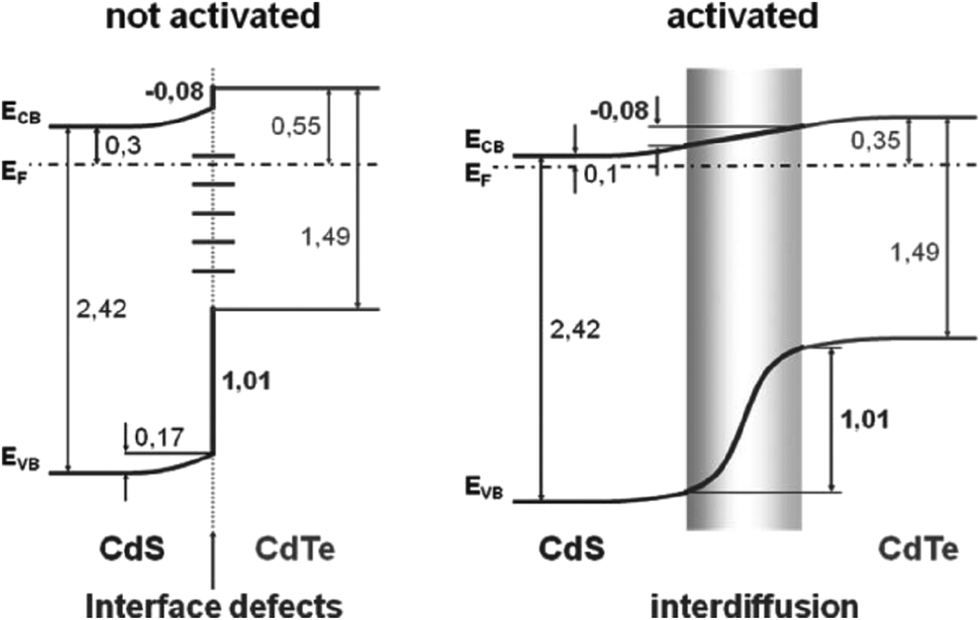 | ||
| Fig. 12 Band energy diagram of the CdS–CdTe interface prepared by physical vapor deposition before activation (left) and after activation (right) (reprinted with permission from ref. 328; copyright @ 2005 Wiley Interscience). | ||
| CdCl2 (solid) + O2 (gas) + CdTe (solid)⇔ TeCl2 (g) + 2CdO (solid) | (2) |
The presence of TeCl2 vapor would increase the surface mobility of both Cd and Te and hence promote CdTe recrystallization.
Polycrystalline films inherently show non-uniform stress in the film but a uniform stress value after in situ CdCl2 treatment.310 It should be noted that air-annealed CdTe film does not show any significant grain growth and is likely that the presence of CdCl2 during annealing induces a sintering mechanism within the CdTe film that acts to decrease the intergrain pore size and increase the average grain size.293 Thus, the combined effect of improvement in microstructure, layer interdiffusion and electronic properties with a junction activation step improves the device efficiency. However, excess CdCl2 can also enhance the surface oxidation (TeO2) and roughness of the film.283
The junction activation step may or may not induce recrystallization of CdTe depending on the initial stress of the material and nature of the deposited layers.362 The CdTe films deposited by CSS do not undergo recrystallisation upon annealing with CdCl2,363–365 but reduce the structural defects and affect the GBs, resulting in higher effective acceptor concentration.101 The grain growth for smaller CdTe grains after CdCl2 treatment will be assisted by the fluxing agent of CdCl2 and strain present in the small grains. The small grains are easy to reorient and coalescence occurs leading to drastic grain growth. However, for a densely packed larger grain size having a low concentration of defects and low stress state,363–365 the junction activation step may not produce sufficient energy to reorient the grains.243 Interestingly, CdTe deposited at low temperature via a CSS and radio frequency magnetron sputtering method experienced identical physical changes with the activation step.343 The CdCl2 treatment did not influence the grain size of CdTe obtained via a nonvacuum chemical molecular beam deposition method (CMBD) but a significant impact on the mobility and carrier concentration was observed.366 Thus, grain growth of CdTe after activation depends on the initial grain size of CdTe; the smaller the grain size, the more significant is the grain growth. It is proposed that chlorine would increase stress in grain boundary regions where the recrystallisation process is likely to start during the heat treatment.343 Only those species arriving or attaching to the surface near the grain boundary take part in the grain growth process.324 In particular, the grain boundary region becomes heavily p-doped due to preferred grain boundary diffusion and segregation of chlorine and oxygen.45 The diffusion coefficient of Cl in CdTe for GBs is known to be five orders of magnitude larger compared to bulk CdTe.126 Hence, samples with high grain boundary length per unit area are most likely to exhibit rapid grain growth.324 During activation, small CdTe grains are transformed directly into the vapor phase and recrystallize to a better organized CdTe matrix:95,257
| CdTe(s) + CdCl2(s) ⇒ Cd(g) + Te(g) + Cl2(g) ⇒ CdTe(s) + CdCl2(s) | (3) |
The presence of Cl2 favors the CdTe crystalline growth by means of local vapor phase transport. In this way, small grains disappear and the CdS–CdTe interface is effectively reorganized. The grain growth of CdS during excess CdCl2 treatment may introduce stress at the TCO–CdS interface, resulting in the loss of adhesion between two layers or lead to film blistering or peeling.
After treating CBD-CdS with CdCl2, the following defect reactions arise:367
| VS (in CdS) + CdCl2 → CdCd + 2ClS | (4) |
The other possibility is that CdCl2 incorporation generates VCd and ClS in CdS:
| CdCl2 → VCd + 2ClS | (5) |
The out-diffusion of Cd from CdS to CdTe takes place because CdTe is Cd deficient, causing VCd at the CdS surface:
| CdS + VCd (in CdTe) → VCd (in CdS) + CdTe | (6) |
CdCl2 treatment may introduce Cl-rich precipitates into CdTe but their influence on the device performance is not known. The chlorine-rich residue surface will be chemically and thermally stable and thus etching with HNO3 is generally required to obtain a chlorine free surface.368
Castaldini et al. have enumerated 12 defect trap levels for Cl dopants in CdTe and have shown the importance of A centers [VCd–ClTe] and mid-gap traps.369 Valdna et al.370 have shown that (Tei2−–ClTe+)− and or (VCd2––ClTe+)− shallow acceptor complexes stabilize the high p-type conductivity of CdTe films. The CdTe treated with CdCl2 introduces three defects; VCd, ClTe and their defect complex VCdClTe.367 During the annealing of CdTe with CdCl2, it is possible that one CdCl2 molecule can generate one VCd and two Cl atoms in Te sites (ClTe). The diffusion length (L) of minority carriers was same (0.31 μm) for both untreated and CdCl2 treated cells. This means that L is not affected by the grain size and is probably given by the carrier lifetime in the grain bulk. The value of L might be limited by a deep level in the band gap of CdTe.77
The improvement in p-type conductivity of CdTe and electrical properties during the junction activation step is attributed to complex interaction between CdCl2, impurities and sulfur interdiffusion. From a theoretical point of view, chlorine is predicted to promote further p-type doping of CdTe via a VCd–ClTe complex with an ionization energy of 30 meV below that of VCd.351 Hence, chloride diffusion into grains and within a border region of larger grains during the CdCl2 treatment promotes p-type conversion of CdTe layers. The as-deposited CdTe film is p-type with a resistivity of 104 to 105 Ω cm originating from native stoichiometric defects like VCd, which drops to 7–100 Ω cm after CdCl2 treatment.374,375 The low concentration of chlorine (1016 to 1018 atom cm−3) leads to low resistance p-type conductivity, while a semi-insulating property was observed for a higher concentration of Cl (>1019 atom cm−3) in a CdTe lattice.370,376 It is also reported that photoconductivity of the n-CdS (and p-CdTe) film increased when heated in CdCl2 solution, due to the generation of non-equilibrium charge carriers from the non-ionized acceptor levels positioned at 0.07 eV higher than the VB top.377 In addition, the current transport mechanism switches from tunneling/interface recombination to recombination in the depletion region (thermal emission) attributed to the elimination of electrically active interface states by a mechanism that is not possible by simple annealing, as revealed by both temperature dependent J–V characteristics and spectral response measurements under reverse bias.352,375 This change in current transport mechanism was found to be associated with: (i) an increase in heterojunction barrier height; (ii) a decrease in dark leakage current; (iii) an increase in cell Voc.352 Some authors ascribe the effect at least partly to the reduction in the volume fraction of material influenced by GBs due to grain growth.172 DLTS measurements showed that depletion region recombination probably occurs through a large density of deep states at Ev + 0.64 eV arising from a (VCd–Cl)− defect complex as a result of interaction between VCd introduced by heat treatment and chlorine from CdCl2.352 These deep acceptor traps, though important factors for diode current transport, will have a non homogeneous distribution inside the CdTe layer which is detrimental to Voc.352,378
During the fabrication of a cell, the junction activation step “dominantes” over the back contact fabrication, as the former exerts significant impact on the surface composition and chemical nature of the interfaces.379 The thickness of CdCl2 plays a major role; if the layer is too thin, the effect of CdCl2 will not be apparent and an optimal Voc is difficult to obtain for a very thick CdCl2 layer.189 The CdCl2 treatment decreases the resistivity of stoichiometric CdTe (1:1 of Cd–Te) film owing to an increase in the carrier concentration from 2.3 × 10⁷ to 4.7 × 1012 cm−3. This is because oxygen occupies tellurium vacancy VTe2+ and as a result the donor level (Ec −0.48 eV) passivates and acceptor level (Ev +0.15 eV) activates. The resistivity as well as carrier concentration does not change much for Cd-rich and Te-rich CdTe obtained by CMBD, indicating that the junction activation step may not be necessary for CdTe obtained by this novel method.366
Junction degradation was investigated using a CdTe layer with a high concentration of VCd.367 In the PL spectra, as-deposited CdTe exhibits a sharp peak at 1.59 eV, a broad band at 1.44 eV and a satellite peak at 1.57 eV. The peak at 1.44 eV corresponded to electronic transition from the CB edge to VCd and its broadness indicates that the distribution of a deep energy level by VCd is not well-defined. The peak at 1.59 eV is a bound exciton transition peak which is slightly lower than the band gap of CdTe (1.61 eV at 10 K) and the peak at 1.57 eV is a satellite bound-exciton transition peak due to phonon scattering.227,380 Upon treatment with CdCl2, the peak at 1.44 eV is shifted by 5 meV (1.435 eV) due to structural relaxation with CdCl2 treatment, and a new signal at 1.455 eV was attributed to the transition from CB to a VCd–ClTe defect. After treating with a Cu2Te back contact, a new peak at 1.52 eV was observed due to defects caused by Cu atoms in the Cd site (CuCd), which shifted to 1.53 eV because of CuCdClTe defect formation.367 The junction activation step resulted in the modification of the energy diagram in the recombination levels. For an untreated cell structure SnO2/CdS/CdTe/Ni, two types of recombination levels with lifetimes τ1 = 16 μs and τ2 = 30 μs were observed at 80 K.377 The recombination levels with τ1 characteristic time are stable in the whole temperature range, but decrease weakly at 200 K reaching a value of 12 μs. However, τ2 reaches a maximum of 50 μs at 140 K and decreases to 25 μs at 300 K (Fig. 13). For treated cells (heated in CdCl2), τ3 (13 μs) at ≤140 K decreases to 5 μs at 200 K due to the shift of quasi Fermi level that transforms the two hole capture levels into recombination levels. The τ4 reaches a maximum of 37 μs at ∼260 K followed by sudden decrease thereafter, and τ5 remains active for temperatures ≥210 K reaching 180 μs at 300 K, accounting for the high photoconductivity of the devivce.377 The junction activation for CdTe/CdS/SnO2/ITO/glass indicates a diffusion process at two interfaces: (i) interdiffusion of CdS and CdTe at the CdS–CdTe interface; (ii) 5% Cd diffusion into entire SnO2 layer.381 The diffusion of Cd into the SnO2 layer reduced the band gap of SnO2. The ΔEv of 0.7 and 2.0 eV was found for activated CdS–SnO2 and CdTe–SnO2 interfaces, respectively. The activation resulted in a Fermi level shift in both CdS and CdTe by 0.2 eV towards the CB. It is important to note that such changes in doping of CdS and CdTe were not observed when they were deposited separately from each other into an SnO2 electrode. Hence, interdiffusion of CdTe and CdS must be responsible for the observed change in electronic properties. In addition, CdCl2 treatment changed the surface morphology of the CdTe layer while SnO2 and CdS films were almost unaffected.381
 | ||
| Fig. 13 The lifetime of the non-equilibrium charge carriers in the temperature interval from 80–300 K. Energy levels active in the un-annealed CdTe films; curves 1 and 2. Recombination levels active in the presence of CdCl2 structure; curves 3, 4 and 5 (reprinted with permission from ref. 377; copyright @ 2005 Elsevier). | ||
In the as-deposited film, diffusion of sulfur into CdTe is very significant compared to Te diffusion into CdS.384 The interface width increased from 0.24 to 0.36 μm after annealing at 380 °C, followed by the shift of the metallurgical junction peak towards the CdTe side. There was a progressive loss of sulfur from CdS and an increase in Te concentration at the surface that influenced each other. With further annealing at 400 °C, width increases to 0.48 μm with significant loss of sulfur leaving a Cd rich surface (Fig. 14). The significant loss of sulfur at 400 °C was due to both diffusion and sublimation, indicating that the degradation of the heterojunction and the influx of Te was not sufficient to occupy all VS sites. The net effect after annealing decreased the concentration of anions. The change in sulfur concentration exhibits two distinct features: a broad region corresponding to the fast diffusion across the interface and into the CdTe film, while a slow diffusion was found to be independent of temperature. The increase of interface width because of CdTexS1−x alloy formation was supported by XRD analysis, where the diffraction peaks shifted towards higher angles (Fig. 15).384
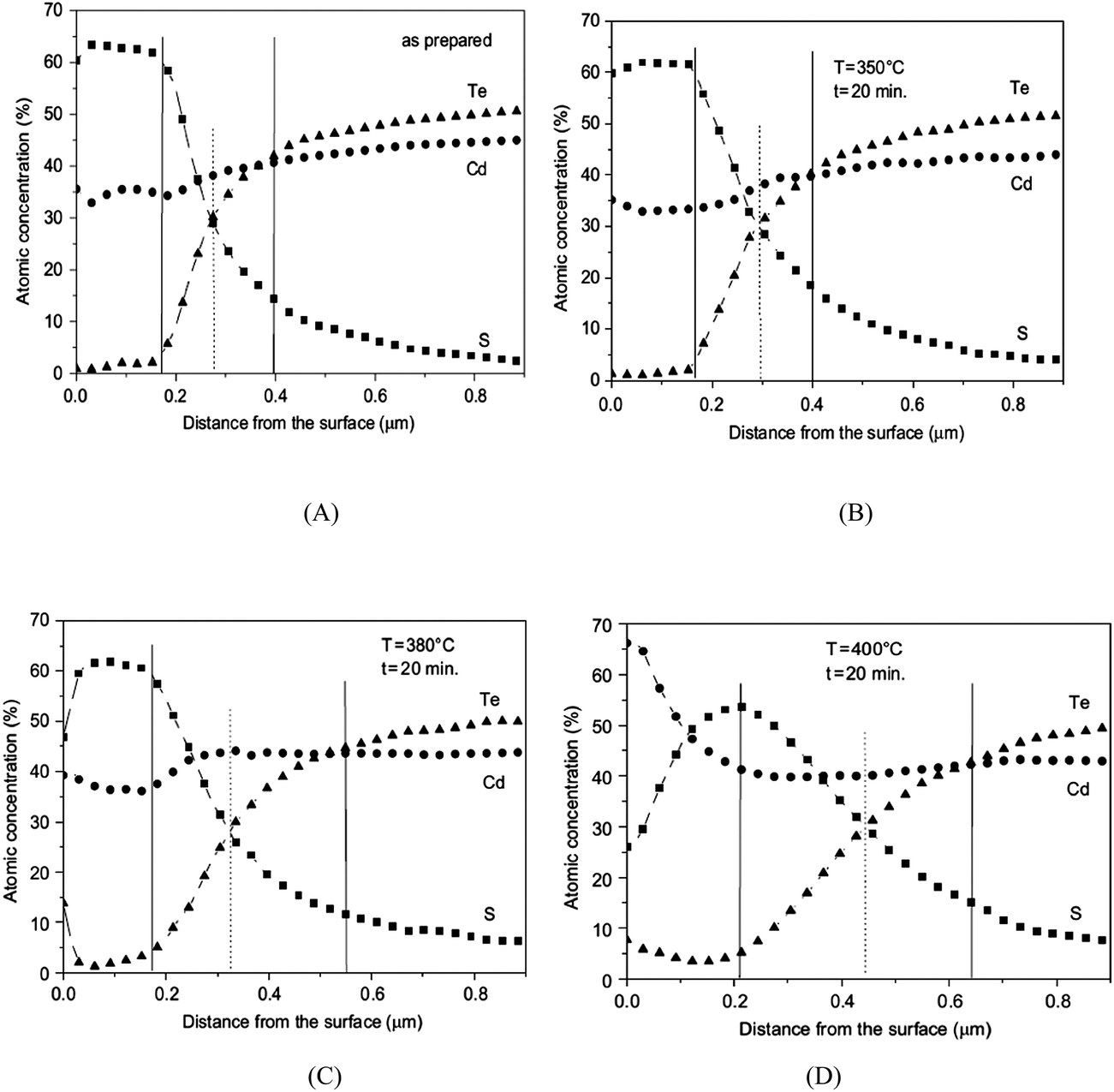 | ||
| Fig. 14 Auger depth profile of CdTe/CdS device fabricated under different annealing conditions (reprinted with permission from ref. 384; copyright @ 2007 Elsevier). | ||
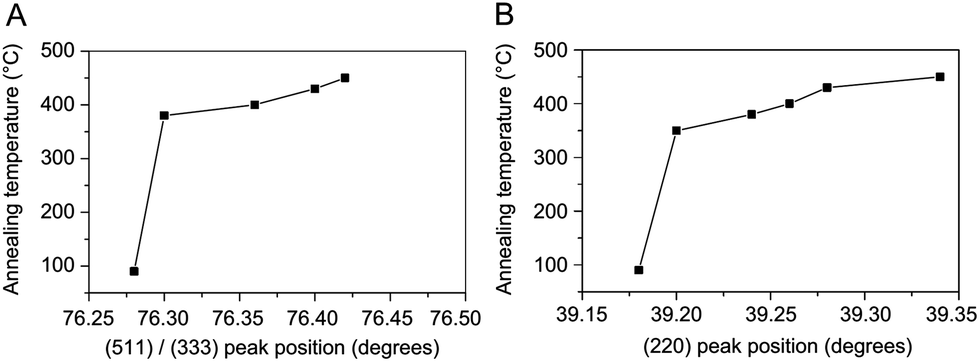 | ||
| Fig. 15 Graphs showing the shift of the characteristic peaks of CdTe due to the formation of the alloy CdTe1−xSx. (A) (511)/(333) peak and (B) the (220) peak (reprinted with permission from ref. 384; copyright @ 2007 Elsevier). | ||
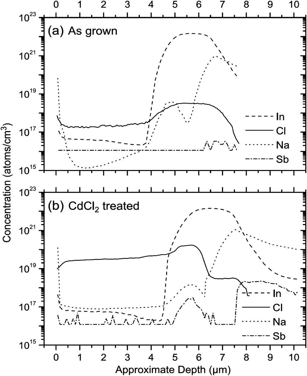 | ||
| Fig. 16 Species that are present in the CdCl2 starting material: quantitative SIMS depth profiles of In, Cl, Na and Sb impurity atoms for the CdTe/CdS/In2O3:F/glass structures without (a) and with CdCl2 treatment (b) (reprinted with permission from ref. 387; copyright @ 2005 Elsevier). | ||
The relative concentration of several isotopes, as revealed by SIMS analysis, followed the order: 16O > 35Cl > 12C > 34S through the main body of the CdTe matrix.127 It is known that CdTe has a propensity for self compensation and hence effective dopant concentration may be an order of magnitude lower than the total concentration of impurities. SIMS analysis of solar cell after the removal of glass substrate showed an increased concentration of Cl, Na and Sb impurities in CdS after CdCl2 treatment, while Pb, O, Sn and Cu conserve the same concentration. Furthermore, Zn, Si and In had a slightly lower concentration after CdCl2 treatment. Sodium was concentrated at the CdS–CdTe and TCO–CdS interfaces, while the peak concentration shifted to the CdS layer during processing conditions.389 During CdCl2 treatment at 400 °C, there is a possibility of formation of compounds such as ZnCl2, InCl3 and SiCl4. The SiCl4 is gaseous at this temperature, while ZnCl2 and InCl3 have a high vapor pressure compared to CdCl2. This is the most likely explanation for the observed decrease in Zn, Si and In concentration after CdCl2 treatment.389 In addition, CBD-CdS also revealed a high concentration of carbonaceous species in the cell matrix. The presence of carbon would have adverse effect on chloride diffusion and associated recrystallisation of CdTe.127 Alkali metals are mobile, with small activation energies below 1 eV for diffusion in CdTe.390 Thus, care is necessary to avoid sodium concentration, which can diffuse from the glass substrate as contamination during the activation step. Boyle et al.127 found that cell efficiency was in the range of 6.9–7.8% despite the presence of several impurities from CBD-CdS; no correlation between performance and impurity distribution could be found. This result further strengthens the use of polycrystalline thin films for solar cell applications at lower costs by utilizing lower grade source materials. Emziane et al.391 reported that nearly 83–91% of impurities present in the CdCl2 precursor serve as potential dopants in CdTe. The electrically active impurities in CdTe are generally considered to be IA (Li, Na, K), IIIB (Al, Ga, In, Tl), VB (N, P, As, Sb), VIIB (F, Cl, Br, I), and IB (Cu, Ag, Au) elements in periodic table. The behavior of I A and I B elements is complicated because of their smaller atomic or ionic radii with high diffusivity and hence might leave the lattice position to serve as interstitial donors. The possible relationship between impurity profiles, solar cell efficiency and stability together with reproducibility needs to be further investigated.
| CdTe(s) + 2Cl2(g) → CdCl2(s) + TeCl2(g) → CdTe(s) + 2Cl2(g) | (7) |
This reaction favors CdTe film recrystallization and increases its crystalline quality. After heat treatment, the sample is kept under high vacuum in order to re-evaporate CdCl2, which could be deposited on the CdTe surface. Both HCF2Cl and CdCl2 treatment showed a similar grain growth mechanism, but with a different impact on GBs; treatment with Freon gas leads to compact structures with reduced GBs, while CdCl2-treated layers exhibit wider and more pronounced boundaries. Freon gas treatment may not relax compressive stress generated by lattice and thermal mismatch between CdTe and CdS as they do not diffuse much through the GBs.361
The device glass/ITO/ZnO/CdS/CdTe/Cu–Mo activated with a mixture of HCF2Cl and other gases exhibit an efficiency in the range of 14.0–14.6% and this remains unchanged even after the first month of its manufactured lifetime.392 In this study, CdS was treated in an oxygen atmosphere before CdTe deposition, which suppressed the interdiffusion and resulted in better control over the formation of intermixed CdSxTe1−x near the junction. The decrease of reverse current was observed after annealing in HCF2Cl gas.393 The efficiency of this cell was found to vary with the partial pressure of HCF2Cl and the cell structure treated at 40 mbar exhibited a 14.8% efficiency. The diode factor of 1.8 was observed for untreated cells, indicating that recombination currents dominate the junction transport mechanism due to a high density of interface defects. The diode factor reduces to 1.2 for HCF2Cl (40 mbar partial pressure) treated cells suggesting decrease in the density of interface recombination centers. The cell treated with 50 mbar showed again a sharp behavior by increasing the diode factor to 1.8 as a consequence of junction degradation. The activation energy for the impurity diffusion decreases by increasing the HCF2Cl partial pressure due to the enlargement of band formed by [VCd–ClTe] complexes.302,394 CL studies revealed that some Cl (or F) impurities are incorporated inside CdTe grains, where a high VCd concentration could favor the formation of a (VCd–ClTe) complex.302 The only drawback in using HCF2Cl, which is an ozone depleting agent, but this can be recovered and reused in a closed loop during industrial production. The activation process with Freon gas is not universal, and it depends on the fabrication process of CdS (or CdTe) thin films. Despite extensive study, the change in fundamental material properties induced by the junction activation step leading to improvement in device performance is far from being understood.
5. Properties of CdCl2-activated and heat-treated CdTe/CdS solar cells
5.1 Changes in textural properties
The CdTe deposited on a glass substrate via CSS at low temperature (340 °C) showed preferential orientation along the {111} direction, while high-temperature (520 °C) processed CdTe preferred {400} crystal plane nucleation. After activation with CdCl2, the strong {111} texture of low temperature CdTe converts to a {400} texture, similar to the non-activated sample.395 In another study, a {311} plane orientation was observed for the as-grown films, while heat/CdCl2 treatment resulted in the orientation of {111} at the expense of the {311} plane, indicating a recrystallization from a nearly random grain orientation to a pronounced {111} texture.100,382 Samantilleke et al.396 reported that as-deposited CdTe wurtzite film showed a marked improvement in {002} reflection after annealing in air followed by CdCl2 treatment and disappearance of Te diffraction peaks (Fig. 17). At 150 and 300 °C, CdTe grown on HVE-CdS layers exhibit a {111} orientation before and after CdCl2 treatment. On the other hand, CdTe grown on CBD-CdS preferred a {111} orientation at 150 °C, while {111}, {311} and {422} orientations were observed at 300 °C.397 The creation of new grains due to disintegration of some large grains was a consequence of the relaxation of excessive strain in the lattice. The coalescence of small grains into larger ones is caused by CdCl2 sintering flux with annealing at high temperature. Because of the composite nature of CdTe layers, XRD peaks corresponding to crystallographic planes of as-deposited CdTe grains and regenerated grains will be observed.397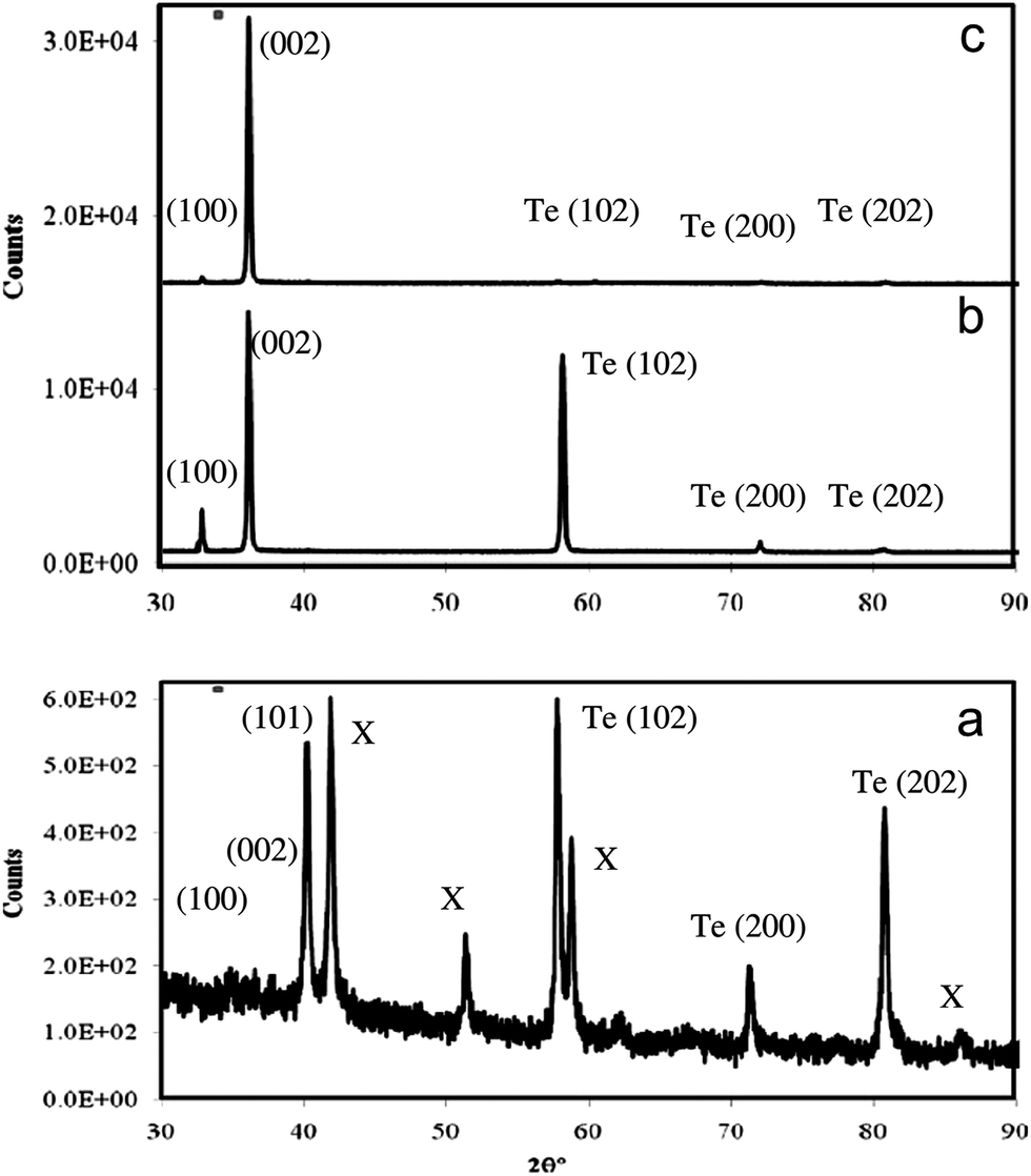 | ||
| Fig. 17 XRD patterns of CdTe for as deposited (a), annealed in air for (b) 3 h and (c) 2 h following CdCl2 treatment. The peaks marked ‘X’ arise from FTO electrode (reprinted with permission from ref. 396; copyright @ 2011 Elsevier). | ||
The CdTe film deposited on a CdS/ITO/glass substrate via radio frequency sputtering exhibit a zincblende structure with a preferred orientation of {111} and {511} crystal planes.319 A weak {002} hexagonal plane of CdS appeared with dry CdCl2 treatment, while the same was not observed for the wet CdCl2 process. Regardless of CdCl2 treatment, several peaks corresponding to the {220}, {311}, {331} and {422} planes of cubic phase appeared and intensified with an increase in annealing temperature at the expense of the {111} plane. Paulson and Dutta318 reported that in the presence of sufficient CdCl2 vapor pressure, CdTe grains grow preferentially in the cubic phase with {111} orientation. It is also reported that as-grown and vacuum-evaporated thin film CdTe showed a biphasic nature that was cubic and hexagonal, while CdCl2-treated CdTe showed only a cubic phase with the preferred {111} orientation.345 Thus, the relieved strain energy may contribute to grain growth with {111} growth in CdCl2 treated films, whereas films without an activation step will have a high density of imperfections in the lattice that may not have preferential grain growth. Major et al.138 reported that preferred orientations {111} were lost for films with smaller grain size. This mechanism was due to: (i) randomly oriented nucleation; and (ii) fast growing orientation which dominated by outgrowing the slower ones, taking place only when islands were present in high densities and to their co-operative interactions. Such a difference was attributed to the influence of chamber pressure during CdTe grain growth via CSS. It is therefore inferred that growth conditions, rather than the grain size itself control the preferred orientation. From the above discussions, it is clear that texture changes and crystallographic rearrangements are not identical for all films, indicating that the number of grains of different orientation depends on grain size, temperature and preparative methods, in addition to activation treatment.398
5.2 Efficiency of annealed solar cells
During the preparation of CdS or CdTe, annealing removes excess Cd or S/Te leading to reduction in Cd/Te or Cd/S content at the surface. Hence the improved device performance during the annealing process is due to the increase of the depletion layer width via removal of recombination centers in the form of Cd and Te/S energy levels. The annealing of CdTe/CdS layers with front contact ITO/polyimide under an oxygen atmosphere showed 11.4% efficiency (Voc = 765 mV, Jsc = 20.9 mA cm−2 and FF = 71%), while as-deposited cells had only 8.5% (Voc = 746 mV, Jsc = 19.3 mA cm−2 and FF = 59.1%) which was attributed to the high stability of annealed films. Despite the higher sheet resistance of the ITO layer, a maximum current density was obtained for the annealed films.399 The efficiency of the solar cell was increased after annealing (300 °C, 25 min) due to the crystallization of the CuxTe1−x layer, which improved the conductivity of the back contact.237 The current transport across the junction is controlled by a thermally activated process for in situ cleaning of CdS prior to CdTe deposition, while interface recombination via tunneling was observed without in situ cleaning of CdS. This was due to a high density of interface states in the latter compared to former.250 With an in situ cleaning technique, solar cells of about 1 cm2 area have achieved an efficiency of 10.5%. Thermochemical data indicated that in situ cleaning of CdS via heating in a hydrogen atmosphere (400 °C, 20 min) will vaporize a thin layer of CdS from the substrate surface and reduce any oxides on the surface of the source material. Thus the clean interface will minimize the extrinsic interface states.250 Layer-by-layer mass spectrometry analysis of heterostructure showed that annealing in air for 10 min leads to the redistribution of Cd, resulting in excess Cd aggregation at the CdTe surface and formation of VCd in bulk CdTe.296 The lengthy process of heating (400 °C, >10 min) results in the formation of CdO and CdTeO3 at the layer surface generating VCd in the bulk CdTe layer without passivating the non-radiative recombination centers.16,203,400 Since VCd in CdTe serves as an acceptor, generation of these vacancies gives rise to inversion in the conducting type of the graded gap from n-CdTe1−xSx to p-CdTe1−xSx, which means that p–n junction moves to CdS1−yTey/CdTe1−xSx surface. Short term annealing, however, results in only indium diffusion from the In doped n-CdS layer and in this case the p–n junction shifts to the CdTe region. The diffusion length is a function of the lifetime and mobility of carriers relating to recombination and trapping within the grains and or GBs serving as recombination centers for minority carriers and trapping centers for majority carriers. Since annealing promotes the incipient fusion of smaller crystallites, it reduces the grain boundary density increasing the diffusion length.401 The CdTe grown on CdS/SnO2/ITO at a substrate temperature of 340 and >500 °C showed superior cell characteristics, as these temperatures render a favorable film morphology with compact layers consisting of larger grains with a size of the film thickness and a minor concentration of voids and craters.3265.3 Efficiency of CdCl2 treated solar cells
The efficiency of solar cell with CSS-CdTe deposited at low temperature (420–474 °C) was tuned by changing the degree of saturation in CdCl2–CH3OH from 50 to 75%. With increase in the degree of saturation, the efficiency was increased at a given temperature. In contrast, an opposite trend was observed with high temperature deposited CdTe solar cells (620 °C). The efficiency was almost same for the above device for a 100% saturated solution (Table 2).343 This result showed that depositing CdTe via CSS at low temperature can be beneficial for device fabrication as it eliminates the problems associated with the softening of the soda lime glass substrate and consequent diffusion of impurities into the film structure. The CdCl2 treatment drastically improved the efficiency for CdTe deposited at low temperature, while only a marginal improvement was observed for the high temperature CdTe deposited cell.343 The conversion efficiency, 11.5%, increased after dry CdCl2 treatment at a temperature of 400 °C and decreased thereafter, which is caused by the change of interface states between CdS and CdTe due to interdiffusion, and also due to the increased grain size with a decrease in the number of GBs (Fig. 18).319 However, wet CdCl2 treatment was not effective for grain growth and reproducible results were not obtained. The efficiency increased from 7.1–14.1% for a glass/ITO/CdS/CdTe/C/Ag device with a decrease in CdCl2 treatment temperature (T-CdCl2) from 460–415 °C, which was correlated to homogenization of the spatial distribution of excitons bound to the acceptor states of CdTe or impurities leading to optimized p-type conversion of CdTe.351 On the other hand, when T-CdCl2 is kept constant, the efficiency decreased with increase in substrate temperature >630 °C during CdTe deposition.351 Vapor chloride treatment of CdTe in O2 ambient showed a high FF of 72.5% compared to cells that were heated in inert He (64.4%) and H2 (68.5%) ambients. The J–V feature of oxygen-annealed devices during the CdCl2 treatment has been found to affect the consumption of CdS and the defect structure of CdTe.147,313 The solar cells exhibit maximum Voc and Jsc after CdCl2 vapor treatment for 60 min (Table 3).275 For this treatment time, CdCl2 enhances the crystalline quality of the intermixed region by decreasing non-radiative recombination centers and only a minor consumption of CdS layer takes place. The decrease in efficiency for longer treatment times was attributed to: (i) excess diffusion of Te into CdS forming CdSyTe1−y, which reduces the high energy portion of the device spectral response; (ii) consumption of CdS layer and formation of CdTe/ITO microjunctions; (iii) compensation of excess Cl; and (iv) an intermixed phase that gradually disappears, as revealed by PL studies.275,402 In contrast, FF attained a maximum value at 30 min suggesting that the optimization was observed over a broad range of 30–60 min. Such behavior could be attributed to CdS, which received only thermal treatment prior to CdTe deposition rendering improper mixing of CdTe and CdS.275 In another study, a device treated with CdCl2 (400 °C in air, 10 min) resulted in high efficiency compared to other annealed films treated in the range of 20–60 min (Table 4).403 For very low annealing times, CdCl2 treatment promotes the sulfur diffusion into CdTe to form a CdSxTe1−x alloy near the interface. The 1.5 eV band in untreated CdTe shifts to 1.445 eV after CdCl2 treatment, indicating a change in the dominant PL recombination pathway. It is likely that the CdCl2 promoted sulfur diffusion near the interface passivates the grain boundary and increases the relative luminescence efficiency by reducing the non-radiative recombination centers. For a very long annealing time, diffusion of sulfur towards the back surface of the cell takes place implying that all the CdS is consumed and uniform solid solution results.403| Film | CdCl2 treatment | V oc/mV | J sc/mA cm−2 | FF (%) | η (%) | |
|---|---|---|---|---|---|---|
| T/°C | CdCl2–methanol (%) | |||||
| Low temperature (420–474 °C) | — | — | 416 | 5.6 | 31.0 | 0.7 |
| 400 | 100 | 689 | 12.9 | 38.6 | 3.4 | |
| 400 | 50 | 617 | 18.1 | 42.1 | 4.7 | |
| 400 | 75 | 741 | 18.3 | 46.6 | 6.3 | |
| 420 | 50 | 747 | 21.0 | 54.0 | 8.5 | |
| 420 | 75 | 745 | 20.8 | 57.4 | 8.9 | |
| High temperature (620 °C) | — | — | 710 | 9.6 | 60.9 | 8.4 |
| 400 | 100 | 631 | 11.3 | 52.9 | 3.8 | |
| 400 | 50 | 798 | 19.9 | 66.7 | 10.6 | |
| 400 | 75 | 720 | 20.2 | 48.5 | 7.1 | |
| 420 | 50 | 773 | 19.8 | 56.0 | 8.6 | |
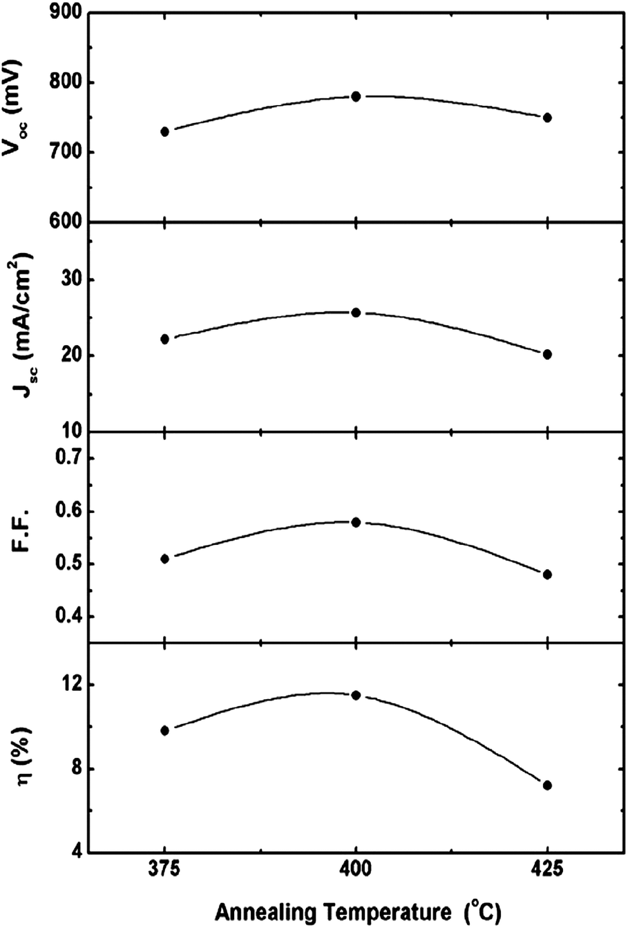 | ||
| Fig. 18 Influence of annealing temperature with evaporated CdCl2 layer on CdTe/CdS solar cell parameters (reprinted with permission from ref. 319; copyright @ 2011 Elsevier). | ||
| CdCl2 treatment in minutes | J sc/mA cm−2 | V oc/mV | FF (%) | R sh/Ω cm−2 | R s/Ω cm−2 | η (%) |
|---|---|---|---|---|---|---|
| 15 | 9.7 | 578 | 39.1 | 146 | 25.7 | 2.2 |
| 20 | 13.7 | 595 | 43.5 | 133 | 17.1 | 3.5 |
| 30 | 14.7 | 618 | 52.4 | 112 | 13.7 | 4.7 |
| 40 | 16.4 | 641 | 35.7 | 247 | 23.7 | 3.7 |
| 60 | 18.5 | 663 | 40.8 | 137 | 20.0 | 4.7 |
| 70 | 17.0 | 470 | 30.2 | 20 | 21.6 | 2.4 |
| 90 | 10.0 | 191 | 25.7 | 55 | 18.0 | 0.5 |
| Annealing time/min | V oc/V | J sc/mA cm−2 | FF (%) | η (%) |
|---|---|---|---|---|
| As grown | 0.55 | 13 | 31 | 2.1 |
| 10 | 0.70 | 22 | 57 | 8.4 |
| 20 | 0.72 | 21 | 51 | 7.9 |
| 30 | 0.67 | 18 | 53 | 6.6 |
| 40 | 0.64 | 20 | 53 | 6.7 |
| 60 | 0.62 | 19 | 50 | 6.0 |
The solar cells with SnO2 front contact and Ni back contact showed high FF when dipped in CdCl2 compared to MnCl2 and CsCl (Table 5).404 The poor current for MnCl2 and CsCl was due to the lower carrier mobility in the absorber. Thus the roles played by Mn and Cd atoms on the surface and or inside CdTe layer are different in that Cd reduces the film resistance, while opposite was observed for Mn. However, a low FF of 0.48 for CdCl2 treated solar cells was mainly due to the parasitic back barrier, which serves as secondary parasitic diode connected in series but with opposite polarity to the main photocurrent-generating diode. Such a barrier has a distinct signature; reduced FF along with a “rollover” of J–V curves that turns down in the higher voltage range. Though the Voc increased slightly at lower temperature, the rollover becomes much more pronounced as the temperature is reduced and the back contact barrier becomes progressively larger compared to kT implying the Jsc temperature dependence is due to the back barrier effect extending well into the power quadrant.404 The heat treatment increased the efficiency from 1.2–3.6% mainly as a result of an increase in Jsc from 6.5 (for as deposited cells) to 15 A cm−2 without a change in the Voc (0.55 V) and FF (39%). However, CdCl2 treatment resulted in a drastic improvement in the cell parameters (Voc = 0.65 V, Jsc = 26.5 A cm−2 and FF = 56%) with an efficiency of 10% via switching the current transport mechanism from tunneling to a thermally activated process.375 As-deposited films did not exhibit a back contact effect due to their high resistivity. The Rs decreased from 76 to 16.7 and 6.7 Ω sq−1 for heat- and CdCl2-treated films, respectively, while leakage resistance although decreased for heat-treated films (106 Ω sq−1), was enhanced after CdCl2 treatment (180 Ω sq−1) compared to as-deposited films (150 Ω sq−1) accounting for improvement in the FF of these cells. The collection efficiency of CdCl2 treated cells showed a well-formed junction compared to as-deposited and heat-treated films.375
| Cell parameters | Not treated | Dipped in different chloride solutions and annealed in air | ||
|---|---|---|---|---|
| CsCl | MnCl2 | CdCl2 | ||
| J sc/mA cm−2 | 0.28 | 5.9 | 12.5 | 18.9 |
| V oc/mV | 380 | 460 | 390 | 820 |
| FF (%) | 0.21 | 0.27 | 0.26 | 0.48 |
| η (%) | 0.02 | 0.4 | 1.3 | 7.4 |
Temperature dependent I–V analysis in the dark indicated that above 280 K, the dominant current transport mechanisms in Au–CdTe/CdS–TO (as-grown) (G1) and Au–(annealed) CdTe/CdS–TO (G2) devices are determined by interface state recombination, while current transport was limited by the depletion region recombination for Au–(CdCl2 dipped and annealed) CdTe/CdS–TO (G3).405 Below 280 K, multistep tunneling was the dominant transport mechanism for the above devices. The high-frequency C–V studies for G1 and G2 revealed that the capacitance values were independent of reverse bias in the entire temperature range due to the presence of a thin insulation layer at the CdS–CdTe interface, while the G3 device showed a dependence on voltage (Fig. 19). Thus, the C–V variation observed in device G3 is attributed to the narrowing of depletion width and improvement in junction interface via decrease of interface state density. The DLTS revealed that majority carrier hole traps in G1 localized at Ev + 0.19, Ev + 0.20, Ev + 0.22, Ev + 0.30 and Ev + 0.40 disappeared after CdCl2 heat treatment, resulting in the formation of new hole trap at Ev + 0.45 eV. The low efficiency of vacuum-deposited solar cells investigated in this study was attributed to the presence of complex or extended defects originating from VCd and impurities like gold or chlorine.405
 | ||
| Fig. 19 The C–V characteristics for typical devices from groups (a) G1, (b) G2 and (c) G3 measured at various temperatures and 1 MHz frequency (reprinted with permission from ref. 405; copyright @ 2004 Elsevier). | ||
The solar cell treated with CdCl2 and Cu2Te/Au back contact showed a conversion efficiency of 12% which was lowered to 6% after subjection to thermal stress. However, the performance was increased to 9.5% by applying a reverse bias to thermally stressed cells.367 The stress test revealed that Cu atoms occupying CdS shield from the light intensity penetrating into the CdTe layer. The stronger light-shielding at the shorter wavelength region suggests that deep-level Cu impurity is located at 1.55 eV below the CB, so that electrons can be freely activated from Cu states to CB. The copper atoms from the back contact diffuse through the CdTe layer and are incorporated into the CdS layer, which result in less n type states and reduce the junction potential.367
6. Improvement in the efficiency of CdTe/CdS solar cells by varying the properties of individual components
6.1 High efficiency reported solar cells
The annealing of CdS in an H2 atmosphere prior to CdTe deposition exhibits an efficiency of 15.8%.406,407 The use of a high substrate temperature for CdTe deposition via CSS promotes the formation of an interfacial layer, shifting the electrical junction to a p-CdTe layer and improving the cell parameters. The back contact involved chemical etching with a 0.1% Br2–CH3OH solution or an NP etch followed by the application of a doped graphite paste. The decrease in CSS substrate temperature during CdTe deposition and increase of CdS thickness was detrimental to performance. However, Voc was relatively independent of substrate temperature in the range of 540–625 °C.406,407 The CTO (Cd2SnO4)/ZTO(ZnSnOx)/CdS:O/CdTe/back contact structure exhibited an efficiency of 13.9% and 16.5% with an infrared transmission of 50%.205,256 The CdS:O window layer has a higher optical band gap (2.5–3.1 eV) and smaller grain size compared to a conventional CdS film resulting from its high oxygen atomic concentration. The CdS:O also had a high photoconductivity ratio, demonstrating its high material quality and lower defect density. In addition, oxygen content reduces tellurium diffusion from CdTe into CdS and improved QE in the lower wavelength region. By integrating a ZTO buffer layer, the probability of forming a localized CTO/CdTe junction was significantly reduced.256 In addition, the ZTO buffer served as an “etch stop” layer during back contact formation and greatly reduced the shunting problems. The interdiffusion between ZTO and CdS during CdCl2 treatment may relieve the stress at the ZTO–CdS interface and improve their adhesion to the substrate. The use of a resistive or buffer layer in addition to conductive TCO appears to be beneficial, especially for those devices fabricated with thin CdS films. By incorporating a very thin resistive buffer layer, a CdS layer with a thickness of <50 nm could be used that can improve the blue response, CdS film morphology and conversion efficiency.408 Dharmadasa et al.409 reported an efficiency of 18% for a glass/conducting glass/CdS/CdTe/metal device, where the depletion width of the device structure is greater than the combined thickness of the CdS/CdTe layer. Since both the absorber and window layer were n-type, further incorporation of n-type dopant is expected to improve the electrical conductivity of the device structure.6.2 Solar cells deposited on an Mo substrate
Conventional thin film solar cells manufactured on a glass substrate have the disadvantage of weight and the fragile nature of their modules in which glass makes up to 98% of the device thickness and weight.410 Its poor thermal expansivity and conductivity causes thermal gradients and non-uniform device properties on panels with a continuous fabrication process involving high temperature (>500 °C).411,412 Normally, thermal treatment during the cell fabrication reaches the melting temperature of ordinary soda lime glass, causing the rupture of the glass substrate or diffusion of sodium into the cell structure.413 A passivating layer like Al2O3, SiO2 or 1 μm ITO (90% In2O3 and 10% SnO2) is usually deposited to avoid sodium diffusion from the glass substrate.174 As an alternative, solar cells can also be deposited on metal foil or a polymer substrate,414 which results in cost reduction, high material utilization, increased fabrication scalability and more importantly they do not show a “darkening of color” as observed in some glass based cells under particle irradiation. CdTe and Mo have very similar thermal expansion coefficients of 5.0 × 10⁻⁶ and 4.8 × 10⁻⁶ K−1, respectively. Even after annealing (550 °C, 2 h), CdTe does not peel away from Mo foil nor form blisters/bubbles.415 Since high purity Mo can be obtained, problems associated with dopant impurity diffusion into CdTe will be reduced at the elevated temperature.Solar cells deposited on the Mo substrate showed an efficiency of 5.3%.189 A thin layer of Cu and Te film was used as a contact layer between CdTe and Mo. A series of experiments revealed that both CdS and CdTe pretreated with CdCl2 and CdTe annealed in air with double CdS layer (a CdS film of 200 nm followed by annealing and deposition of a second CdS layer with 800 nm thickness) exhibit a Voc of 824 mV compared to other cells wherein CdTe was annealed in nitrogen and CdS (or CdTe) without CdCl2 treatment. The first layer of CdS will be consumed by CdTe due to interdiffusion of tellurium and sulfur across the interface by forming a Cd–Te–S solid state alloy. After the first layer is annealed, it becomes CdTexS1−x, and sometimes it becomes p-type as determined by the four point probe technique.416a The p–n junction is thus destroyed, and is again recovered after the deposition of second layer and further improved after annealing. The enhancement in the presence of oxygen was attributed to its role as an acceptor dopant and its incorporation in both CdS and CdTe passivates the interface states inhibiting the formation of a buried p-CdTe/n-CdTe homojunction.417 These studies further revealed that the depletion layer spans the entire CdS and CdTe film thickness and the cell needs to be conceived as a single junction device instead of three separate junctions (Mo–CdTe, CdTe–CdS, and CdS–TCO).417 The solar cell deposited on a flexible Mo substrate using a thin interlayer Au/Pd alloy annealed at 400 °C showed an efficiency of 3.5%.413 It was assumed that the thickness of the CdS layer decreased during the thermal treatment as a result of CdS sublimation from the surface. The Voc dropped from 0.5 to 0.2 V for the films calcined at 450 °C. The difference in work function of p-CdTe and Mo necessitates for an interlayer that can form a non-rectifying contact between CdTe and Mo.413 Such measures are usually referred to as a back surface field (BSF), which increases the cell performance by reducing recombination at the back contact leading to improved Voc and reduced Rs. In another study, the cell deposited on 100 μm thick Mo foil with a ZnTe:N back contact resulted in 7.06% efficiency. However, such a structure suffered from poor Voc and FF with strong roll-over under forward current because of an inefficient back contact.418 The low efficiency of the solar cells in these cases is caused by the fact that the conventional device structure must be inverted, which restricts device processing and consequently limits the electronic quality of the CdTe layer. Very recently, Kranz et al.416b reported a breakthrough efficiency of 13.6% in the substrate configuration via controlled doping of Cu into the CdTe layer. The addition of 0.8 × 10¹⁵ Cu atoms per cm2 (sub-monolayer, with an equivalent thickness of 1 Å) to 5 μm thick CdTe decreased the resistivity and increased the hole density. Furthermore, this optimum Cu doping resulted in a space charge region of 1.8 μm and caused sufficient band bending close to the CdS to generate a strong electric field leading to effective carrier collection. Although, the substrate configuration allows better control of p-type doping into CdTe matrix in the absence of n-CdS layer, back diffusion of metals during subsequent processing of the window layer and front contact is hard to control.
6.3 Solar cells with different front contact
The solar cell fabricated via radio frequency sputtering at 250 °C using an AZO front contact exhibited a high efficiency of 14.0%, while 12.6% was observed for SnO2:F based solar cells (Table 6).419 The advantages of AZO over SnO2:F as front contact are: (i) the AZO showed excellent transparency in the entire visible spectrum; (ii) a high carrier mobility and low current density as indicated by Hall measurements; (iii) lower sheet resistance of 2.47 at the centre and 3.47 at the edge compared to SnO2:F (7.29 Ω sq−1) resulting in lower Rs. The higher collection in the blue region (360–560 nm) was observed for AZO compared to SnO2:F despite that the deposited layer was 0.13 μm in both cases. Furthermore, interdiffusion of Zn into CdS modifies the AZO–CdS interface during CdCl2 treatment, which increases the band gap and transmittance of the CdS layer.420 The higher QE response (11%) was observed in the visible region (550–825 nm) due to the better transparency of AZO (Fig. 20). An efficiency of 15.4 and 15.6% was obtained for solar cells deposited on borosilicate (BSG) and aluminosilicate glass (ASG) respectively, while the performance was lowered with other substrates using AZO/i:ZnO bilayer front contact (Table 7).421 The high Voc of AZO/i:ZnO/CdTe compared to AZO/CdTe and higher voltage at i:ZnO/CdTe junction together with restriction of current flowing back into weak diodes is attributed to the beneficial effect of the i:ZnO layer with a thickness of 50 and 100 nm.421 Increasing the thickness of the i:ZnO layer leads to UV absorption losses (which results in potential current loss of 0.7 mA cm−2), narrowing the depletion layer width and hence reducing the collection efficiency in the longer wavelength region (685–830 nm). In contrast, a sprayed AZO of 3.2 μm thickness exhibits a high Voc and lower efficiency of 12.1% without antireflection coating compared to sputtered AZO.422 The average value of >11% measured for 22 fabricated solar cells highlights the high homogeneity of the sprayed AZO layer and the feasibility of deposition in solar cell applications.422 An efficiency of 13.5% was reported for high-vacuum evaporated solar cells with a thick AZO/i:ZnO bilayer deposited on soda lime glass, despite the large content of sodium in the glass substrate.128 This is caused by the superior diffusion barrier properties of the thick bilayer due to both increased thickness as well as large grain size. In contrast, application of a thin buffer barrier resulted in widened GBs for CdTe because of significant sodium diffusion deteriorating the cell performance.128| TCO | V oc/mV | J sc/mA cm−2 | FF (%) | η (%) | R s/Ω cm2 | R sh/Ω cm2 |
|---|---|---|---|---|---|---|
| SnO2:F | 820 | 20.7 | 73.96 | 12.6 | 3.9 | 1822 |
| ZnO:Al | 814 | 23.6 | 73.25 | 14.0 | 3.16 | 989 |
 | ||
| Fig. 20 QE curves of CdTe/CdS solar cells using ZnO:Al and SnO2:F front contact (reprinted with permission from ref. 419; copyright @ 2004 American Institute of Physics). | ||
The application of low cost APCVD graphene films grown on Cu foil at 1000 °C by varying the H2–CH4–Ar gas rate as front electrodes with a ZnO barrier layer resulted in 4.17% efficiency (Fig. 21).423 The choice of graphene stems from its suitable work function (4.42 eV) close to FTO (4.4 eV). ZnO improved the continuity and crystallinity of CdS film and also prevented unwanted forward leakage current enhancing the lateral current collection. The device without a ZnO barrier showed an efficiency of 2.81% due to a poor interface between CdS nanoparticles and the graphene film resulting in poor wetting and incomplete surface coverage. This allows forward leakage current to the graphene front contact, simultaneously reducing the efficiency. Graphene films exhibit an extremely high carrier mobility (up to 600 cm2 V−1 s−1) compared to commercial TCFs with a sheet resistance in the range of 1150–220 Ω sq−1 and better optical transparency of 97.1–83.7% in the 350–2000 nm spectral region depending on the number of layers. The number of layers was found to be 1, 2, 4 and 7 for H2 gas flow rate of 10, 30, 50 and 80 in sccm in H2-CH4-Ar.423
 | ||
| Fig. 21 Schematic diagram and J–V features of a solar cell with graphene front electrode (reprinted with permission from ref. 423; copyright @ 2011 Wiley-VCH). | ||
Among the various TCOs, such as Sn-doped In2O3, F-doped In2O3 (FIO), Cd2SnO4, Ge-doped In2O3, SnO2 and Zn2SnO4 devices, the FIO-based device showed the highest efficiency of 14%. The sputtering atmosphere used for the deposition of FIO was a mixture of Ar, Ar + H2 and CHF3 (Table 8). In addition, smooth and transparent FIO had resistivity of 2.5 × 10⁻⁴ Ω cm and 1000 Å of this material were sufficient to passivate sodium atoms which would otherwise diffuse into the film from soda lime glass.424
| TCO | Sputtering gas | Resistivity/Ω cm | Transparency 400–800 nm | Stability of the devicea | Reproducibility |
|---|---|---|---|---|---|
| a Stability of device on different TCO after the aging process on ‘open circuit conditions’, under 10 suns, at a temperature of 110 °C for 2 h. | |||||
| ITO | Ar + 4% H2 | 2 × 10⁻⁴ | ≥80% | Good | Good |
| SnO2 | Ar + 20% H2 | 8 × 10⁻⁴ | 80% | — | — |
| IGO | Ar + CHF3 + H2 | 2 × 10⁻⁴ | 85% | Very good | Very good |
| Cd2SnO4 | Ar + 50% O2 | 2 × 10⁻⁴ | 85% | Very good | Very good |
| Zn2SnO4 | Ar + 50% O2 | 10−2 | ≈90% | — | — |
| INO:F | Ar + CHF3 + H2 | 2.5 × 10⁻⁴ | ≥85% | Excellent | Excellent |
A sufficiently thick and large grained AZO layer as TCO can effectively suppress sodium diffusion from soda lime glass and protect the device from degradation.128 High electron mobility and better transparency of AZO in the wavelength region <900 nm makes it an attractive candidate for CdTe solar cells.418 The main disadvantage of AZO is its instability at high temperature due to aluminium diffusion or inter diffusion across the ZnO–CdS interface during the process conditions and illumination.419 Graphene as a front electrode would be quite encouraging because of the limited availability of indium, the high production costs and poor performance as a result of deterioration and brittleness due to ion diffusion.425 Transparent conducting oxides are very important for the design of solar cells not only for their electro-optical properties but also for their favorable interaction with CdS. It is also useful to take advantage of the different properties of two TCOs by forming a bilayer consisting of a highly conducting and very thin layer of suitable materials. This structure can minimize forward current through pinholes in the window layer and eliminate the formation of shunting microjunctions.5
6.4 Influence of CdS layer thickness on device performance
The device efficiency increased with decrease in dCdS from 114 to 95 nm without change in Voc and FF (Fig. 22).271 This was ascribed to an increase in Jsc with a reduction in dCdS that improved the spectral response in the shorter wavelength region (λ < 590 nm). For dCdS < 85 nm, large decreases in Voc and FF were observed without change in Jsc, resulting in poor efficiency. The increased recombination of charge carriers in PV active layer lowers the infrared response with the reduction of CdS thickness. The electroreflectance measurements indicated that interdiffusion rate will be low for very small dCdS, thus increasing the lattice mismatch and interface states at the CdS–CdTe interface.271 The deterioration of CdTe1−xSx inhibits the grain growth of CdTe and increases the dark current at low bias voltages, resulting in low FF and Voc. The dominant influence of CdTe1−xSx with dCdS < 85 nm lies in changing the diode properties of the cell rather than its trivial optical properties as window layer.271 The solar cells with a CSS-CdS film thickness of 160 nm showed superior performance (10.9%) compared with different thicknesses such as 200, 130 and 180 nm at various substrate, source temperatures and times along with a copper-free back contact.395 This suggests that neither a high nor reduced CdS thickness could contribute to enhanced performance. The high efficiency was attributed to a rise in the substrate temperature from 380 to 420 °C during the deposition leading to a more homogeneous and dense CdS film.395 The efficiency was further increased to 12% after fabricating the cell with a copper back contact. A thinner CdS film (130 nm) was used as substrate to deposit a CdTe film at 340 °C, while a thicker CdS film (180 nm) was used to deposit CdTe at 520 °C indicating that the optimal temperature for CdTe deposition depends on the CdS film thickness. In addition, the junction activation treatment for high-temperature deposited CdTe was annealing at 380 °C for 25 min, and 400 °C for 30 min in the case of low-temperature CdTe.395 The device efficiency was improved by introducing an In (or Sn)-oxide buffer layer onto the TCO film and Voc > 0.84 V and FF > 75% was achieved.426 The In-oxide layer breaks off the influence of ITO during the heat treatment and reduces the strain or dislocation at the ITO–CdS interface in the vicinity of the CdTe/CdS junction. The increase of the diode factor without In-oxide buffer was explained by the decrease of QE in the entire wavelength region with forward bias, while such junction recombination dependence on forward bias voltage was not observed with an In-oxide buffer layer. A significant improvement in FF was not achieved due to the thermal expansion coefficient of glass substrate. However, by using a two-step CdS formation method, the efficiency was improved on a soda lime glass substrate due to the evaporation of CdS which promoted the interdiffusion of sulfur and tellurium (Table 9). In addition, fabricated cells using a two-step CdS film did not reduce its QE in the wavelength region of 500–550 nm (Fig. 23). A high efficiency of 15% was also obtained with a corning glass substrate.426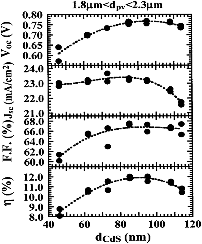 | ||
| Fig. 22 Photovoltaic performances as a function of CdS layer thickness (reprinted with permission from ref. 271; copyright @ 2003 Elsevier). | ||
| Glass substrate | In-oxide buffer | 2-step CdS | V oc/V | J sc/mA cm−2 | FF (%) | η (%) |
|---|---|---|---|---|---|---|
| Corning 7059 | 0.747 | 24.2 | 58.9 | 10.7 | ||
| ✓ | 0.842 | 25.0 | 75.9 | 16.0 | ||
| ✓ | 0.805 | 25.8 | 71.5 | 14.8 | ||
| ✓ | ✓ | 0.824 | 26.0 | 72.0 | 15.4 | |
| Sodalime | 0.572 | 22.8 | 60.3 | 7.88 | ||
| ✓ | 0.830 | 22.4 | 67.5 | 12.6 | ||
| ✓ | 0.807 | 23.8 | 71.7 | 13.8 | ||
| ✓ | ✓ | 0.819 | 23.9 | 74.1 | 14.5 |
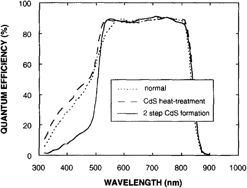 | ||
| Fig. 23 Change in spectral response of the cells fabricated on corning glass by introducing the two step CdS formation method (reprinted with permission from ref. 426; copyright @ 1997 Elsevier). | ||
The solar cell with bilayer (120 + 40 nm) CBD-CdS showed 6.55% efficiency compared to other structures, which were different in the junction activation step.427 CdCl2 treatment was applied after bilayer deposition of CdS to obtain the best device; the first CdS layer at 75 °C for 10 min and the second CdS film was deposited at 40 °C for 45 min to form the bilayer. In others, meanwhile, junction activation was done after first layer deposition of CdS or at each stage of CdS deposition (Fig. 24). The spectral response as a function of wavelength showed a maximum at 600 nm corresponding to the carrier collection generated in the depletion layer due to the strong electric field in this region. A slow decrease for the maximum down to 400 nm indicates that the CdS bilayer is thin enough to allow light-generated charge carriers beyond 510 nm corresponding to the CdS band gap.427 The bilayer CdS comprising of CSS-CdS (bottom) and a second CBD-CdS layer on top showed a high efficiency of 10.1% compared to their individual counterparts.59 The CSS-CdS possesses a larger grain size and more cracks among the GBs, while CBD-CdS has very small grain size. Thus, CBD-CdS covers CSS-CdS producing a complete absence of pinholes and cracks in the multilayer structure. The multilayer film was more homogeneous and compact and its thickness (80 nm) was lower than either CSS-CdS (150 nm) or CBD-CdS (150 nm), thus allowing more photons to pass through the window layer.59 As a window layer, multilayer CdS with uniform grain size distribution exerts a positive effect on the performance of final device structure.
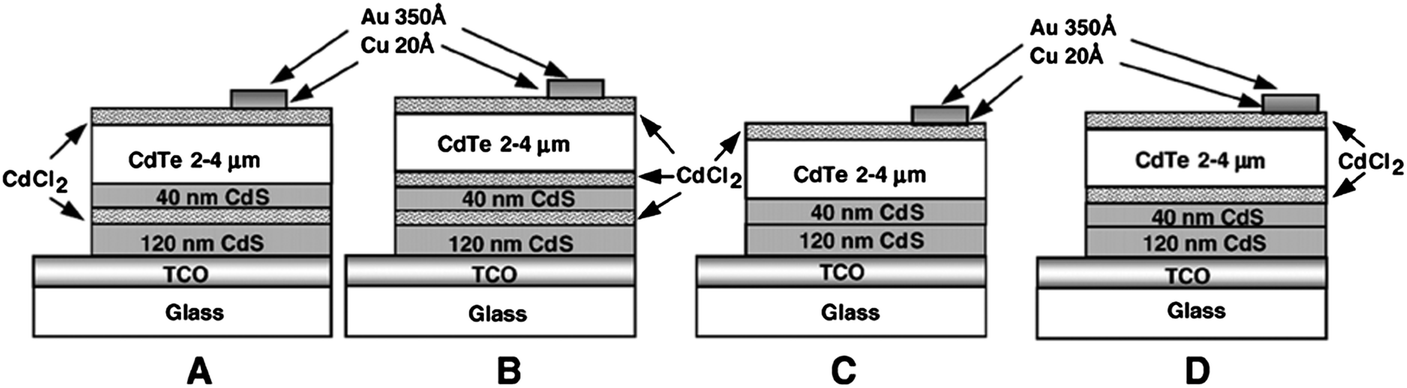 | ||
| Fig. 24 CdTe/CdS solar cell with CBD-CdS bilayers treated with CdCl2 at different stages (reprinted with permission from ref. 427; copyright @ 2008 Elsevier). | ||
6.5 Solar cells with designed window layers
The unoptimized metal/CdTe/CdS/Cd1−xZnxS device grown on TCO coated soda lime glass of 3 mm thickness without an antireflection coating exhibited 10% efficiency due to a better spectral response in the short wavelength region.102 The high electron affinity (χn) of CdS compared to CdTe (χp) eliminates the energy spike at the CdTe/CdS junction. The graded junction between Cd1−xZnxS/CdS exists due to their solubility, in which band gap edges change over certain distance with a finite slope corresponding to the electric field strength. For a thin CdS film, the slope covers the whole of their intermediate layer and coupling with Cd1−xZnxS extends the depletion region throughout the original thickness (Wg) of the CdS layer and up to χp in the CdTe layer (Fig. 25). However, efficiency was lower compared to traditional cells due to the diffusion of Zn and the large lattice mismatch between Cd1−xZnxS and CdTe that pins the Fermi levels restricting their motion, as the displacement of a quasi Fermi level at the interface determines the Voc.102 The increase of Voc from 520 to 830 mV with x varying from 0 to 0.35 was attributed to a reduction in the electron affinity mismatch difference between Cd1−xZnxS and CdTe films at the interface. The lattice mismatch of Cd1−xZnxS with CdTe are 3.7 and 4% for x = 0 and 1 respectively, while a minimum of 0.06% was observed for x = 0.65. The total efficiency did not exceed >4% owing to the high resistivity of the solid solution based films.428 The substitution of Zn into CdS structure improved the efficiency for all the absorber layer thickness (2.25, 1.0 and 0.5 μm CdTe) except for 0.2 μm thick CdTe.121 This reflects the poor performance of the thinnest device as a result of microshorting because of incomplete coverage of 0.2 μm thick CdTe. In addition, the ultrathin film lost the benefit of an improved blue response due to the diffusion of zinc from the window layer associated with CdCl2 treatment. However, reduction in the CdCl2 layer thickness was found to recover the blue response.121 In another study, the Cd0.9Zn0.1S window layer increased the efficiency to 11.42% as compared to only CdS (7.31%).429 The observed increase in Jsc was attributed to a shift in the optical band gap of the window layer from 2.4–2.7 eV, improving the blue response and shifting the absorption edge from 500–400 nm for the ternary alloy window layer. Thus, Cd1−xZnxS/CdS served as suitable window layer similar to CdS to improve the short wavelength response without compromising the transport properties, series and shunt resistance of the solar cell.102 The ZnCdS is used as a window material for the fabrication of p–n junction without lattice mismatch in the device based on CuInxGa1−xSe2,430 or CuIn(SzSe1−z)2,431 CuInSe2 and CuGaSe2.432 However, Cd1−xZnxS film in CdTe devices has some serious drawbacks such as a linear change in lattice parameter with Zn content and electrical resistivity increases from <1 Ω cm to >1010 Ω cm as ‘x’ increases from 0 to 1.433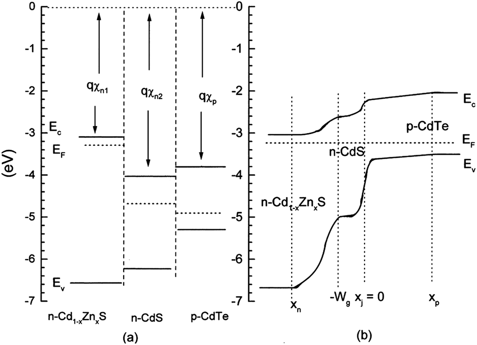 | ||
| Fig. 25 Ideal band diagrams of Cd1−xZnxS/CdS/CdTe system (a) before and (b) after junction formation (reprinted with permission from ref. 102; copyright @ 2000 Elsevier). | ||
The optical transmittance of the strong interface Inx(OOH,S)y/CdS double layer improved significantly in the wavelength region of 500–600 nm with increase in the thickness of Inx(OOH,S)y (Fig. 26). The increase of transmittance in the wavelength range of 400–500 nm was attributed to a reduced thickness of CdS in comparison to the bare CdS (180 nm) film. The efficiency was found to be 9.55% for only CdS and declined to 6.3% for the double layer.434 In addition, Jsc, Voc and FF were not improved with Inx(OOH,S)y because of a lower potential barrier at the window–absorber interface. It was suggested that the CdS in the double layer is less n-type due to Cd out-diffusion from CdS to Inx(OOH,S)y during the CdTe deposition via CSS method at 575 °C. The series and parallel resistances with double layer were larger and smaller, respectively, compared to only CdS. The large J0 with Inx(OOH,S)y suggested that it is necessary to increase the doping concentration of Inx(OOH,S)y/CdS to achieve a more n-type window layer.434
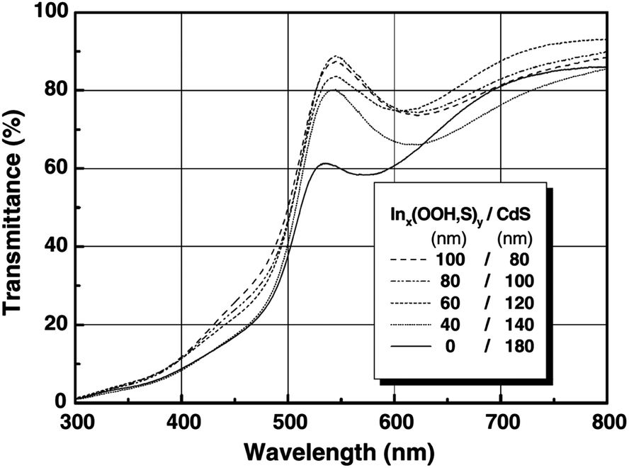 | ||
| Fig. 26 Optical transmittance of Inx(OOH,S)y/CdS double layers with various CdS thickness (reprinted with permission from ref. 434; copyright @ 2009 Elsevier). | ||
6.6 Influence of CdTe thickness on device performance
One of the critical stages in device fabrication is the deposition of a CdTe layer with controlled thickness, composition and stoichiometry. Many advantages were accrued from reducing the thickness of the absorber layer, such as reduced deposition time and post-deposition processing with low environmental impact.435,436 An efficiency of 9.7–11.8% for ultrathin CdTe thickness of 0.7–1.28 μm was found as compared to standard device with 2.3 μm CdTe (13%).120 The cell efficiency remained largely insensitive with CdS thickness within the range of 0.05–0.13 μm. The ultrathin CdTe cells (<1 μm) had a high density of weak diodes and more non-uniformity resulting in poor yield and low Voc. The aniline treatment was found to increase FF and Voc without change in Jsc as a result of reduced shunting. The post deposition process of 10 min CdCl2 treatment, 15 Å Cu back contact and 18 min of back contact diffusion was found to be optimum conditions for the cells with <1 μm thick CdTe.120 Electrodeposited CdTe (1.4 μm, deposited for 3 h) showed higher performance compared to a thin CdTe (1.0 μm, deposited in 2 h) device due to Te segregation on the CdTe surface which improved the back contact.396 A distortion in forward current was observed for the cell with a thin CdTe layer (1.0 μm) leading to a lower FF (0.44) and efficiency (3.3%), while cells with a thick layer (1.4 μm) provided a better ohmic contact at the interface (4.4% efficiency). The Te-rich surface layer is associated with increased conductivity and Te segregation minimizes the use of acidic etchants to create a Te-rich surface. The spectral photoresponse revealed that the IPCE of electrodeposited CdTe declined at lower photon energy, which is a characteristic feature of poor grain boundary passivation despite CdCl2 treatment.396 In addition, solar cells with 1.5 μm CdTe have a larger Jsc by a factor of 913 times higher than 1.0 μm CdTe. It also has a smaller dark saturation current density and a small diode factor both in the dark and light. Thus, a solar cell with a thick CdTe showed more interdiffusion at the CdS–CdTe interface and better PV characteristics.294 The efficiency increased from 0.54–11.34% through tuning the grain size of CdTe from 0.94 to ≥3.6 μm by varying the nitrogen pressure from 2–200 Torr via a CSS method.138 This may be due to a reduced probability of nucleation taking place at elevated pressure, resulting in lower nucleation density. This gives a direct method for the control of grain size in CdTe films with the linear relationship between grain size and pressure: D (μm) = 0.027 × P (Torr) + 0.90. The Rs was optimized at 100 Torr and no changes were observed at 200 Torr, indicating a limiting point at which Rs was no longer dominated by grain boundary phenomena, rather it was influenced by the CdTe/Au back contact interface.138To inhibit the possible recombination loss at the back contact, a wide band gap material like ZnTe (2.2 eV) is proposed, which acts as a BSF to repel the carriers at CdTe/ZnTe and reflect towards the CdTe/CdS heterojunction.437 Both Voc and Jsc for CdS/CdTe/ZnTe increased with the increase in the CdTe thickness, while they decreased for conventional solar cells. In addition, a marginal decrease in efficiency was observed by reducing the CdTe thickness from 2–1 μm with a ZnTe back contact, which is enough to absorb most of the incident photons from solar light (Fig. 27). In contrast, the efficiency decreased below 4 μm thick CdTe and declined drastically for conventional solar cells.253 The efficiency was tuned from 8.0–13.3% by varying the CdTe thickness from 0.25–2.1 μm by careful optimization of magnetron sputtering conditions, CdS and Cu thickness, CdCl2 activation and a back contact diffusion process.122 The efficiency increased from 6.8–12% with the increase in magnetron sputtered CdTe thickness from 0.3–1.0 μm and stability under light soaking was independent of CdTe thickness (0.5–2.5 μm).435 In another study, Voc was enhanced by an increment in absorber thickness from 0.5–2.0 μm CdTe obtained by MOCVD due to enhancement in the photogenerated current as the absorption volume is increased. These devices did not exhibit any roll-over features in light J–V curves, indicating a better ohmic contact formation. The smaller Voc for a thin absorber device suggests an increase of saturation current as a result of the decrease in photogenerated carriers.429 Based on a model, it was proposed that better suitability would be realized by decreasing and increasing the CdS and CdTe thickness, respectively, for NP etched devices. In contrast, this effect was reversed for the devices without NP etching. The physical mechanisms for improved stability with NP etching for a thick CdTe layer may be attributed to the grain-boundary penetrating ability of the etchant.161
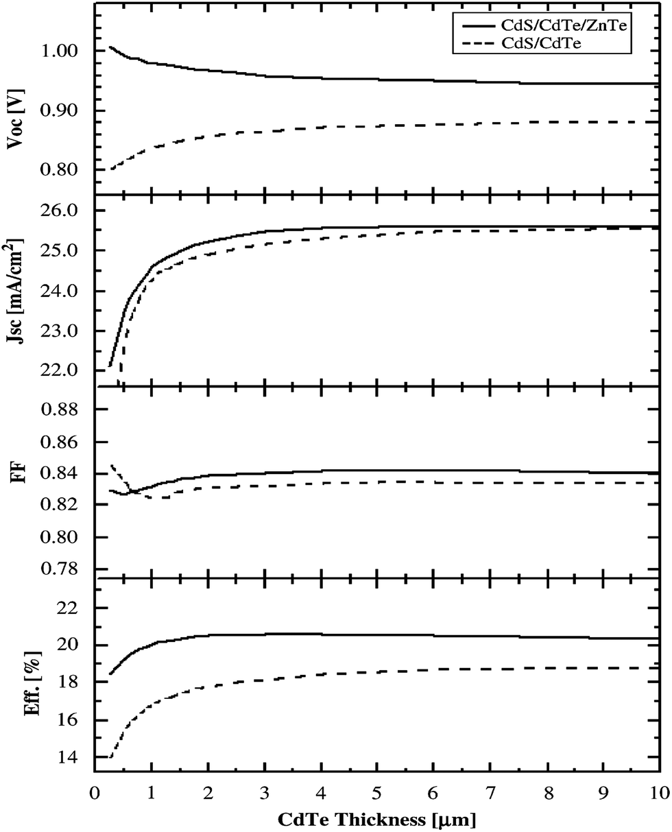 | ||
| Fig. 27 Solar cell performance versus CdTe thickness with and without ZnTe layer (reprinted with permission ref. 253; copyright @ 2007 Elsevier). | ||
The process of back contact formation and surface chemical etching limits the reduction in thickness of absorber layer that can be achieved. In general, thick absorber layers are used to avoid pinholes reaching through the window layer, which leads to shorting from the back contact. In order to reduce the CdTe thickness without compromising the ultrathin quality of the film, a controlled and tunable methodology capable of producing uniform layers must be fabricated. However, a loss of Jsc is inherent with reduction in the absorber layer thickness.
6.7 Effect of doping on device performance
During the device fabrication, oxygen is often present or intentionally introduced during CdTe growth and annealing atmosphere. In the case of both CdTe and CdS, oxygen doping is known to play a role in its morphology, structure, passivation of deep gap states, and hardening against diffusion.275,438,439 In CdTe, the oxygen effect is manifested in grain size, enhanced p-doping and passivation of GBs, while a prominent effect is to make it resistant to in-diffusion of tellurium and out diffusion of sulfur in the CdS.62 In general, CdTe films grown without O2 show a very large grain size and it is relatively easy to form a shunting path by pinholes formed in the film. In addition, oxygen has a notable effect on the nucleation and growth of the CdTe layer; nucleation site density increases with increasing oxygen content, resulting in lower growth rates, smaller grains and a microscopically more compact and dense structure suppressing the possibility of shunting problems. The presence of oxygen during CSS-CdTe deposition also promotes wurtzite CdTe nucleation.62 Valdna et al.440 reported that the film resistivity decreased with the incorporation of a small quantity of oxygen into CdTe matrix, while it increased up to six orders of magnitude at a high concentration of oxygen.The Voc and FF increased as a function of oxygen concentration (oxygen doping into CdTe) showing maxima at 50 and 90%, while a reverse saturation current prevailed for the device fabricated under the lowest O2 partial pressure (Fig. 28).441 The increase of oxygen partial pressure during CSS-CdTe deposition enhanced the net hole concentration and saturated around 3.4 × 1014 cm−3. The change in carrier concentration is consistent with the Voc behavior; higher doping leads to an increase of the built in voltage and consequently enhancement of Voc. The spectral response of the heterojunction decreased with increasing O2 partial pressure in the region of 500–600 nm. The presence of O2 slows down the reaction between Cd and Te atoms such that Te atoms react with CdS to form CdTexS1−x, leading to an improved junction quality. On the other hand, doping with Sb also resulted in a high Voc and hole barrier (net carrier concentration) due to larger band bending at the interface. The Voc reached a maximum at 450 °C and decreased thereafter due to excess recombination because of more Sb reaching the main junction. It was shown that CdTe will be semi-insulating at a very high concentration of Sb in CdTe, as excess Sb substitutes for Cd sites to compensate SbTe and VCd.442 The excess surface Sb or formation of Sb2Te3 can be beneficial for the formation of a stable back contact.
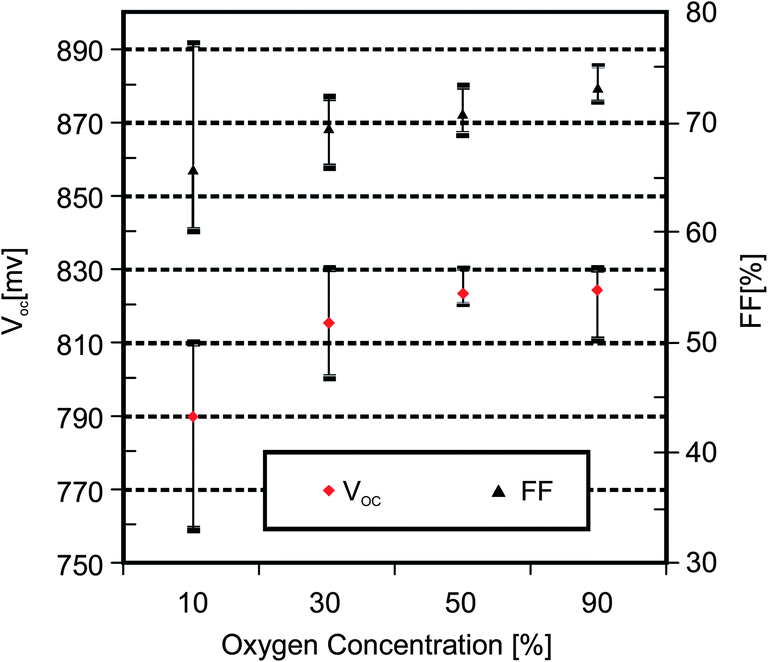 | ||
| Fig. 28 The Voc and FF for CdTe cells fabricated under different oxygen partial pressures (reprinted with permission from ref. 441; copyright @ 2009 Elsevier). | ||
Based on PL spectral studies, the role of oxygen in oxygen/chloride co-processing of the device includes: (i) enhancement in the concentration of ClTe and VCd in CdTe; (ii) promoting the diffusion of Te into CdS under highly oxidizing conditions, yielding Te–O complexes; (iii) acting to fill VS with OS.309 It is also reported that the amount of Cl and O in CdTe is interdependent i.e., the presence of one of them favors the presence of others.443 As-deposited solar cells showed a efficiency of 5.4%, which increased to 6.6% when CBD-CdS was annealed for 5 min in oxygen ambient prior to CdTe deposition. It was hypothesized that annealing of CdS in oxygen ambient hardens CdS against the diffusion of sulfur and tellurium at the interface. Further improvement in the device efficiency to 9.8% was achieved by etching the CdS film with acid to remove oxide formed during the course of annealing.60 The device fabricated on a sapphire substrate using an ITO:F/SnO2 bilayer increased the efficiency from 11.5–14.0% as a result of O incorporation in CdTe.444 The parameters were not affected even after light soaking at a temperature of 100 °C and 20 suns for 20–30 min. The SIMS depth profile indicated that O incorporation leads to an increase in the amount of O (from 1019 to 1020 cm−3) together with doping of electrically active Cl into the CdTe (CdS) layer during CdCl2 activation. In addition, O at the interface region may also decrease the diffusion of Te from CdTe to CdS side. The O and Cl seem to be an electrically active complex within the CdTe, and to a lesser extent within CdS, which improve the device performance.443 In contrast, interdiffusion across the CdTe/CBD-CdS interface was quite low due to the high concentration of oxygen, while it was effective for CdTe/CSS-CdS.445 The presence of oxygen in CdTe did not have any particular effect on the distribution/concentration of impurities like Na, Br, F, In and Sn, while the concentration of Si was lowered, as confirmed by SIMS analysis.443 The importance of CdS–CdTe interdiffusion and O and Cl co-doping is yet to be understood more quantitatively.
The FTO/CdS/CdTe:I/Au cells showed a Voc of 700 mV.446 The iodine dopant enhanced the optical absorption and also improved the electrical conductivity by a factor of 5, indicating a positive effect of n-type doping. The device capacitance was unchanged at 56 pF with applied voltage revealing that the depletion width of device structure is greater than the combined thickness of CdTe/CdS layers. This suggests that a doping concentration <1015 cm−3 in CdTe produces a wider depletion width, greater than the complete device depth. The current–voltage characteristics indicated the presence of a high potential barrier of 1.2 eV with a low ideality factor of 1.40.446 Tran et al.447 also showed that the absence of a mid band gap and ionized impurity scattering centers due to iodine inclusion into CdTe layers, which otherwise results in the loss of short circuit current. The low FF (0.33–0.40) for this device was due to the larger Rs of the doped material. In the case of non aqueous electro-deposited CdS/Cd1−xZnxTe cells, a best performance (Jsc = 26.66 mA cm−2, Voc = 600 mV, FF = 0.42 and η = 8.3%) was achieved for 2 × 10⁻³ M ZnCl2 in a Sb doped CdTe bath.249 The better match of absorber band gap close to the desired optimum value and low Rs of metal–Cd1−xZnxTe contact compared to metal–CdTe resulted in higher efficiency. A Mott–Schottky plot revealed that the carrier concentration and built-in potential was 2.72 × 1017 cm−3 and 1.02 eV respectively. Though the Zn incorporation led to higher Voc, correlation between device performance and Zn mole fraction in Cd1−xZnxTe was not observed. The Rs decreased via incorporation of Sb in the absorber layer under both dark and light illuminating conditions. In addition, spectral measurements were higher in Sb doped CdS/Cd1−xZnxTe cell relative to the undoped cell in the wavelength range of 520–820 nm leading to higher Jsc. The increase in QE on Sb doping is an indicative of better carrier collection.249 Doping of Bi (4 × 1017 cm−3) into CdTe matrix resulted in an efficiency of 8.0%, while doping at low (1 × 1017 cm−3) and high (2 × 1019 cm−3) content was found to be detrimental, which was attributed to the high and low resistivity of doped samples, respectively.448 These results can be understood based on the substitution of Bi in the CdTe matrix; Bi occupies VCd at low concentration serving as donor and VTe at higher concentration acting as acceptor.449,450 Most of the doping atoms have high mobility and tendency to segregate in the absorber layer; the choice of suitable dopants is still a challenging issue.
6.8 Solar cells fabricated with different back contact
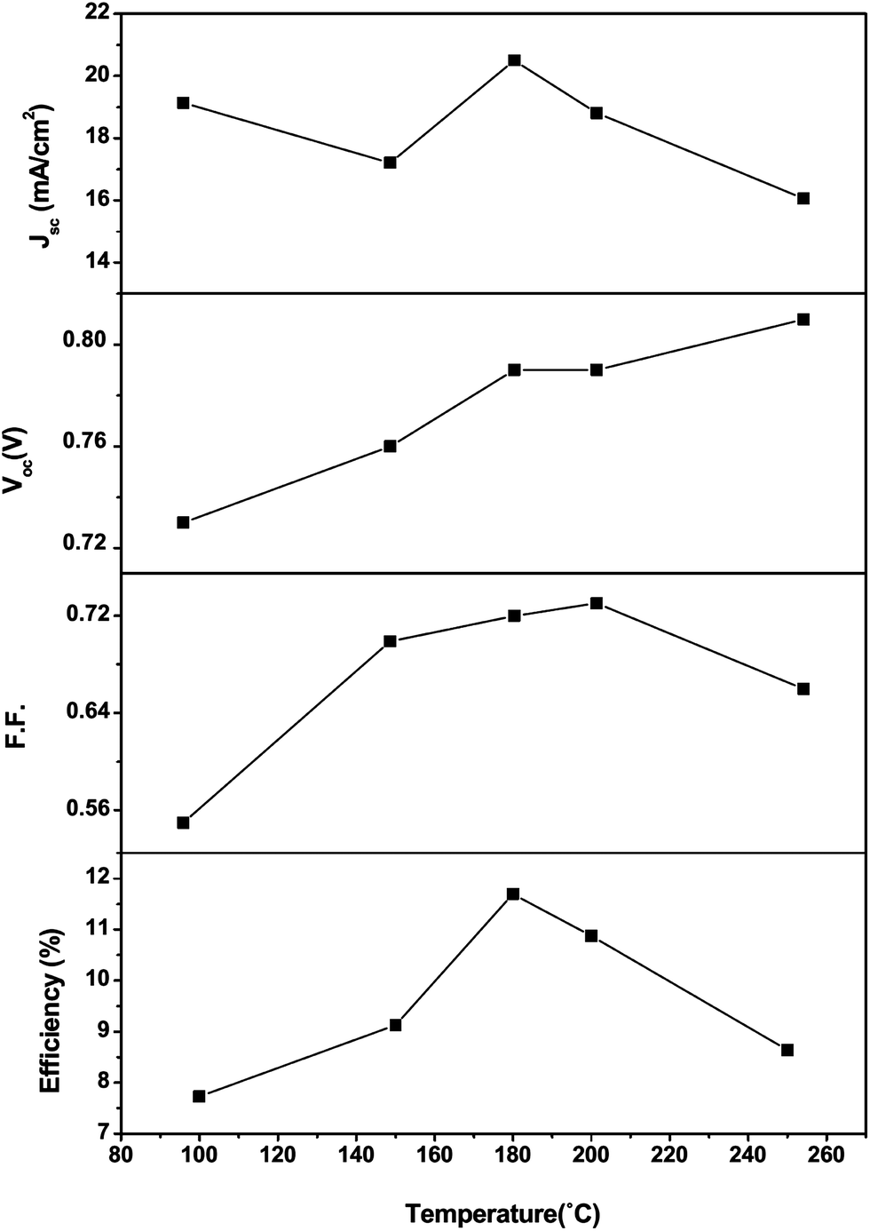 | ||
| Fig. 29 The solar cell parameters of ITO/CdS/CdTe/Cu2Te/Au cells as a function of annealing temperature (reprinted with permission from ref. 451; copyright @ 2003 Elsevier). | ||
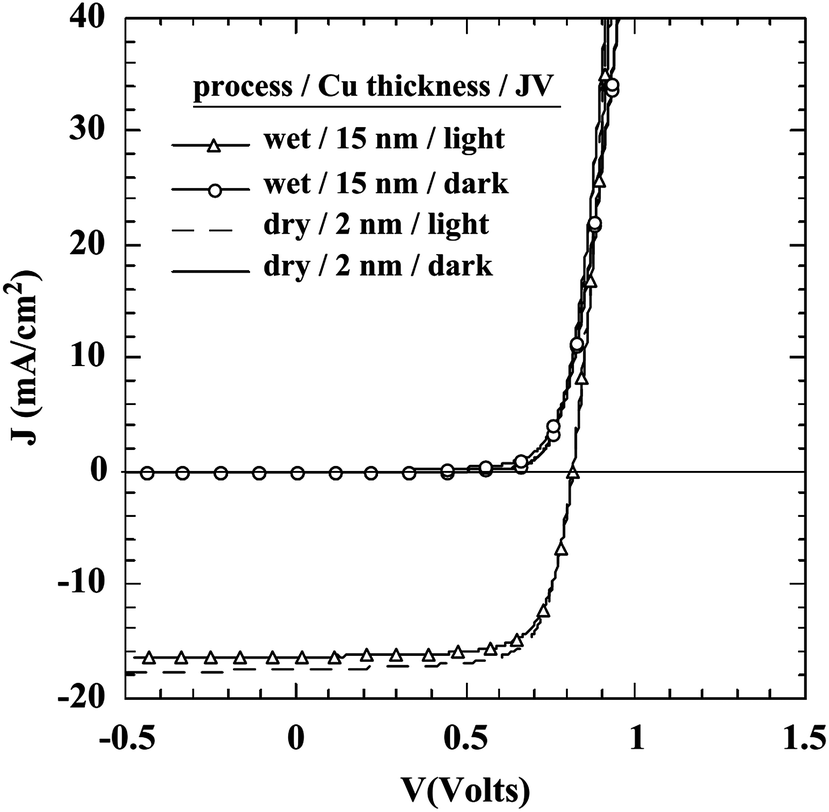 | ||
| Fig. 30 Light and dark J–V curves for devices with wet (15 nm Cu) and dry (2 nm Cu) contact process (reprinted with permission from ref. 228; copyright @ 2005 Elsevier). | ||
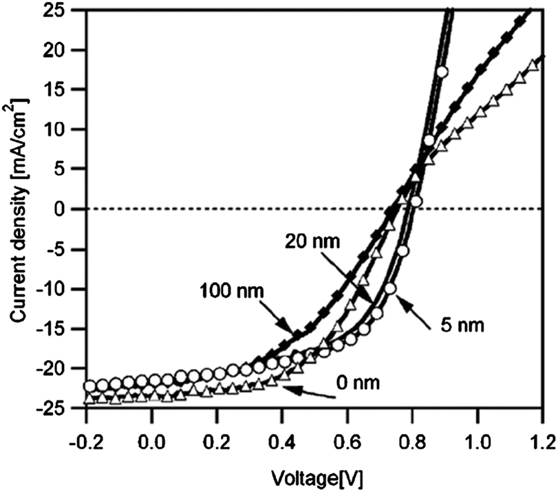 | ||
| Fig. 31 The current–voltage curves for devices with different Cu layer thickness varying from 0–100 nm (reprinted with permission from ref. 452; copyright @ 2008 Elsevier). | ||
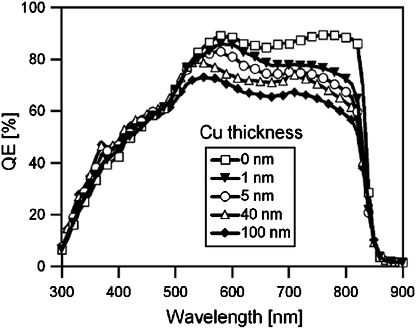 | ||
| Fig. 32 QE curves of CdTe/CdS solar cells as a function of Cu thickness varying from 0–100 nm (reprinted with permission from ref. 452; copyright @ 2008 Elsevier). | ||
Device instability was increased by an increase in Cu content at the back contact, while “interfacial” Cu was not susceptible to device degradation highlighting that Cu substitution at the interface is beneficial while maintaining respectable performance levels.453 The device with Cu showed a drop in Voc after light soaking, while it was restored after annealing. However, the device without copper showed a slight decay at the initial stage and remained largely insensitive to consecutive annealing (Fig. 33).164 Through a procedure of light-soaking for several minutes and low temperature (100 °C), solar cells showed a higher efficiency of 11.4% through decreasing Rs and ionic redistribution in the junction region with a ZnO buffer layer and Cu/Mo back contact. The low carrier density of Cu/Mo contact was sufficient to have a barrier height low enough to create a quasi ohmic contact without the presence of rollover.454
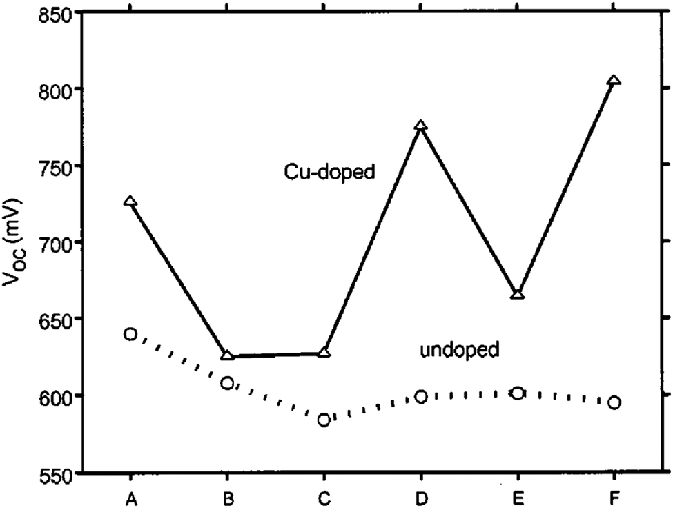 | ||
| Fig. 33 Open-circuit voltage variation with light-soaking stress and annealing for a CdTe/CdS device where the CdTe layer was Cu doped. The points on the graph are: A—initial anneal; B—2 days light soak; C—35 days light soak; D—second anneal; E—2 days light soak after the second anneal; F—third anneal (reprinted with permission from ref. 164; copyright @ 2000 American Institute of Physics). | ||
The device glass/Cd2SnO4/ZnSnOx/CdS/CdTe showed a better FF with a 10 nm Cu thickness. XRD indexed the presence of both CuTe and Cu1.4Te without Cu2Te formation. However, the formation of Cu2Te with large amount of Cu failed to produce a good Rs for the cell. The Cu diffuses into the front region along the grain boundary, resulting in increased shunting at higher Cu levels. In addition, the barrier height was lowest for the device with 10 nm of Cu and increased thereafter (Table 10).455 Cu diffusion from the ZnTe:Cu contact interface increased the net acceptor concentration in the CdTe layer reducing the space charge width of the junction with simultaneous enhancement in current collection.456
| Thickness of Cu/nm | V oc/V | FF (%) | η (%) | J sc/mA cm−2 | Φ (b)/eV |
|---|---|---|---|---|---|
| 0 | 0.733 | 59.8 | 10.1 | 23.0 | 0.53 |
| 10 | 0.797 | 71.3 | 12.9 | 22.7 | 0.48 |
| 60 | 0.783 | 68.0 | 12.1 | 23.2 | 0.50 |
| 95 | 0.767 | 67.2 | 11.7 | 22.7 | 0.51 |
| 110 | 0.761 | 65.5 | 11.1 | 22.2 | 0.52 |
| 130 | 0.725 | 53.2 | 7.3 | 18.8 | 0.54 |
The Ag or Ni deposition on an Cu loaded graphite layer back-contact enhanced the device stability.457 In the absence of graphite, the Ag contact was susceptible for degradation due to the rapid diffusion of Ag and by the formation of metastable resistive shunts. Ni was plagued by Ni3Te2 phase formation that minimized Ni diffusion contributing to the loss of FF. A modest degradation (10–15% reduction in efficiency) was observed with a graphite layer, while there was a significant loss in efficiency (25–45%) for Ag and Ni contacts without a graphite layer. In addition, LBIC studies revealed the formation of micro non-uniformities with stress in Ag- or Ni-only devices, resulting in ohmic microshunts and poor collection of charge carriers due to the diffusion of these metals. Thus, the graphite layer served as a diffusion barrier preventing the migration of these metals from the back contact. The graphite paste contained polyacrylic acid (PAA) polymer at 70% by weight when dried. PAA is a “super absorbent polymer” and is used in cation exchange resins because the acidic hydrogen on the carboxylic functionality can be readily exchanged with several metal cations. The Ag and Ni cations are known to exchange quite readily, and hence the ability of PAA to bind metal cations must be the underlying reason for the enhanced stability of solar cells.457 The device with graphite/Ag (or Ni) showed a similar initial performance of 66% FF, which was reduced in the absence of a graphite layer (Fig. 34). The net current density estimated via C–V measurements for only Ag as the back contact is twice compared to others even before and after stress (Fig. 35). In the case of other back contacts like graphite/Ag, graphite/Ni and only Ni devices, a Te-rich interlayer between CdTe and back contacts effectively “getters” Cu from the graphite paste mixture in the course of annealing and serves as a source of Cu with subsequent stress. However, this finite (200–300 nm) Cu source outdiffusion is augmented by a much larger source of Ag in the form of a very thick (50–100 μm) Ag paste layer for an Ag-only contact. This constant replenishment of Ag into the device is likely to be responsible for the smaller decrease in carrier density with stress in the Ag-only case.457
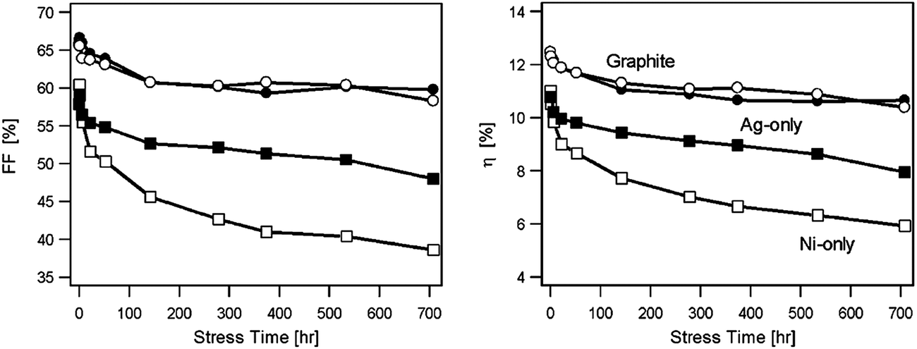 | ||
| Fig. 34 Fill factor and efficiency as a function of light illumination stress time for devices with different back contact; graphite/Ag (–●–), graphite/Ni (–○–), Ag only (–■–) and Ni only (–□–) (reprinted with permission from ref. 457; copyright @ 2006 Elsevier). | ||
 | ||
| Fig. 35 (a) Capacitance versus voltage measurement, and (b) carrier density as function of distance from the junction before and after 707 h of stress (reprinted with permission from ref. 457; copyright @ 2006 Elsevier). | ||
A low Rs and high FF was achieved for the large area thin film (1376 cm2) solar cell submodule with CdTe thickness of 3–5 μm and an Ag paste loaded graphite back electrode. For a CdTe thickness of <3 μm, pinholes occur, leading to a higher leakage current with a drop in FF and Voc.458 High quality and uniform film thickness of the TCO, CdS and CdTe layers contribute to an efficiency of 10.5 and 8.4% for a large-area sub-module with aperture area of 1376 and 5413 cm2, respectively. The major cost reduction for this cell comes from the development of TCO film preparation technology, APCSS techniques to obtain the CdTe film and a patterning technology for large-area substrates.458 In another study, a CdTe thin film prepared by APCSS had a large grain size and less crystal defects compared to those grown under vacuum conditions.459 The CdTe film deposited from a dry milled powder source on CdS film showed a better efficiency compared to conventional sources due to the decreased Te and oxygen content in the powder after dry-milling in air for 4 h. Milled CdTe powder is well suited for APCSS as better nucleation and a large grain size CdTe is obtained. In this cell structure, a graphite carbon paste with 7 wt% carbon black powder resulted in a low back contact resistance with a high FF and Voc (Fig. 36). This suggests that carbon black powder enhances the ohmic contact between the CdTe surface and graphite carbon layer. The best cells were obtained from Cu and Pb doped graphite paste containing a mixture of 7 wt% carbon black glass flints mixed in a solvent. By this fabrication, solar cells with efficiencies in the range of 14–15% were obtained over a small area of 1 cm2, while 11% was achieved for large area (5327 cm2) modules.459 This high efficiency was attributed to the high quality of the CdTe/CdS junction and the stable back contact. In these cells, the density of carbon black powder in the graphitic carbon paste for screen printing is a key factor in reducing the Rs with a rough CdTe surface. The APCSS have a few detrimental aspects for low cost PV production such as: (i) a high interdiffusion rate of CdS and CdTe during deposition; (ii) a high temperature resistive glass is required due to high deposition temperature; (iii) a longer deposition time is needed for APCSS compared to vacuum deposition.459
 | ||
| Fig. 36 Variation in the device characteristics with carbon black density in graphite paste (reprinted with permission from ref. 459; copyright @ 2003 Elsevier). | ||
Conductive graphite paste is a good back contact material for CdTe/CdS solar cells. The work function of graphite nearly matches that of CdTe and the highly polarized valence orbitals of Te (6s & 6p) have an intense chemical interaction with the delocalized C 3pz orbitals.460 The CdTe generates a hole and this transfers to the graphite electrode in the solar cell. Though the doped graphite back contact serves as diffusion barrier for Cu migration,379,461 graphite is relatively low-conducting due to its anisotropic electrical conduction. The hole conductivity perpendicular to the graphite layer (30–50 S cm−1) is much smaller compared to in-plane conductivity (106 S cm−1) leading to low carrier collection and high back contact resistance,462 reflecting the weaker interaction between layers (van der Waals forces with a slightly delocalized π to π* interaction). In this context, graphene has recently attracted tremendous attention compared to other carbon based back electrodes due to its robust characteristics, such as exceptional electron/hole carrier mobility and high mechanical strength. Graphene has only in-plane conductivity and multilayer graphene with a perfect hexagonal carbon lattice is expected to have a lower electrical conductivity along the c-direction (perpendicular to graphene layer) than normal graphite.460
The cell parameters obtained for reduced graphene oxide (r-GO), pristine graphene (PG) and boron doped graphene (BG) highlight that BG serves as an efficient back contact (Table 11).460 The PG prepared by a bottom-up approach had fewer defects with a better electrical transport performance than the chemically reduced exfoliated graphene oxide sheets, as evidenced by Raman spectroscopy. The BG had even higher electrical resistance and a higher work function than PG due to the larger density of states generated near the Fermi level. It is known that the Fermi level of graphene doped with 2 atom% of boron and nitrogen shifts by −0.65 and +0.59 eV, respectively.463 Thus, boron doping increased the hole concentration in the VB of the graphene sheet and a large carrier concentration together with a shift in absolute Fermi level was achieved. As an electron deficient dopant, boron increases the work function of graphene allowing it to serve as a better ohmic contact. As expected, the BG cell had higher efficiency of 7.86% indicating that a highly conductive BG can reduce the barrier height to enhance the efficiency.460 However, integrated graphene-based back electrodes still exhibits poor electrical conductivity due to the large resistance from the interface of submicron graphene sheets limiting the charge carrier collection. Further improvement up to 9.1% was achieved with the use of a highly crystalline 3-layer graphene (5 wt% Cu doped graphene) electrode prepared on 3D template Ni foams by the APCVD method (Fig. 37).464 The graphene sheets in the graphene network are interconnected into 3D flexible graphene networks, which eliminate the contact resistance from GBs and promote electrical conductivity. The assembled graphenes exhibit outstanding electrical properties and their conductivities reached up to 550–600 S cm−1. This efficiency remained the same during measurements over a two-month period, which highlights the excellent reproducibility and device stability.464 Feng et al.465 reported a device with a novel 1D Cu nanowire (NWs)/3D graphene back contact with an efficiency of 12.1% compared to the traditional back contact of Cu-nanoparticle-doped graphite (10.5%) and Cu thin films (9.1%). This high efficiency was due to the giant 3D network of graphene, which supplies a more effective hole transportation channel and efficient back contact. In addition, 1D Cu NWs of 100 nm have a large specific surface area and interact effectively with Te atoms to form a stable intermediate layer. In such a situation, a tunnel current conduction mechanism dominates in which the tunnel current increases sharply and overcomes the loss of holes from the barrier. In fact, the formation of stable CuTe at the interface of Cu NWs and CdTe benefits this back contact from the point of thermal stability, while Cu diffusion via the thermal field into the p–n heterojunction reduces the device performance with other back contacts.465 Interestingly, the CuxTe intermediate layer attached to Cu NW/graphene exhibits a CuTe phase with a preferred {001} peak, while those attached to other Cu-doped back contacts showed a Cu1.44Te phase with a {002} peak. The electrical conductivity (16.7 S cm−1) and the carrier mobility (16.2 cm2 V−1 s−1) of Cu (NW)/graphene were higher than Cu particles/graphene and Cu particles/graphite. The cells with Cu NW/graphene were more sensitive to the visible light response (560–685 nm) and QE reached ∼86.5% at 620 nm, while it was reduced to 85.2% for Cu particles/graphene at the same position. However, no such peaks were observed for Cu particles/graphite and Cu thin films. The high QE in the visible light range was ascribed to the highly conducting Cu NWs/graphene that effectively capture holes from CdTe absorber due to the formation of a CuTe phase.465 These results suggest that the graphene-based conducting materials can be explored as novel low cost back electrodes for CdTe/CdS devices in near future.
| Back electrode | J sc/mA cm−2 | V oc/V | FF (%) | η (%) |
|---|---|---|---|---|
| r-GO | 18.38 | 0.685 | 51.6 | 6.50 |
| PG | 20.81 | 0.674 | 52.9 | 7.41 |
| BG | 21.96 | 0.685 | 52.2 | 7.86 |
 | ||
| Fig. 37 (a) SEM cross-sectional image and top-view of the graphene film in the inset. (b) Schematic CdTe/CdS solar cell with a 3D graphene back electrode. (c) Band structure of the graphene-based CdTe/CdS solar cell. (d) J–V characteristics of CdTe/CdS solar cell with graphene back electrode (reprinted with permission from ref. 464; copyright @ 2011 Royal Society of Chemistry). | ||
The J–V curves showed that roll-over in dark and light in forward-bias conditions due to the high back barrier formed between CdTe and Ni layer, while the addition of a 1.2 μm Te layer eliminated the roll-over.155 Though the Te layer was found to increase the efficiency (8 to 10%) and FF (0.35 to 0.55) but lower the Voc (0.82 to 0.74 eV). The current density reached a maximum of 24.8 mA cm−2 as it diminishes the hole injection from the back contact. These cells had a superior current because of their higher blue photosensitivity but an inferior Voc in relation to the absorption band gap.155 Annealing with Ni or NiTe2 as back contact improved the I–V characteristics compared to as-deposited cells and an efficiency of >10% was reported. These cells were susceptible to reversible degradation under storage in ambient air (H2O vapor) and remained stable in dry air. SIMS investigation revealed that Ni movement or accumulation into the device was not observed after thermal stress (200 °C in air for 20 h).466 NA etching improved the FF compared to NP etching due to a smaller series resistance for the device. As a result of the sharp boundary layer by NA etching, a less-extended Cd deficient CdTe boundary layer is formed at the interface region leading to efficient tunneling between CdTe and the Au back contact.173
Romeo et al.274 fabricated a novel solar cell with an Sb2Te3/Mo back contact, which exhibited 74% FF with a conversion efficiency of 14.6%, while 62% FF was observed without CdCl2 treatment. It has been speculated that CdTe grown on an untreated CdS surface results in a poor junction because the smaller CdS crystallite exposes a large surface for CdTe nucleation thus allowing slow transition of CdS to CdTe. A fine grained CdS film can easily mix with CdTe to form CdS1−xTex resulting in a buried homojunction. After treatment with CdCl2, good morphology and compactness favors the formation of a junction, which develops in a few layers with a very small concentration of interface states. CdCl2 with a thickness of 3000 Å deposited by evaporation and annealed for 30 min at 430 °C showed a superior performance compared with other CdCl2 thicknesses. On the other hand, Sb diffuses slightly into the CdTe matrix making a thin p+ CdTe layer in contact with a low resistivity Sb2Te3 film thus facilitating the formation of an ohmic contact.274 These cells did not show any appreciable degradation during a test period of 6 months when kept at 60 °C under 10 suns in open circuit conditions.174 In another study, a solar cell with an Sb2Te3/Au back contact exhibited an efficiency of 13.1% after annealing compared to as-deposited (9.0%), despite the high barrier for hole transport in the former (0.4 eV) against the latter (0.28 eV).467 This efficiency was ascribed to the band-bending from the SbCd+ donor at grain boundaries that facilitate charge carrier separation in the vicinity of GBs. The electrons are drawn into the GB core and flow towards the junction, while holes are transported through the grain bulk towards the back contact. This charge separation leads to reduced recombination and enhancement in the collection of photogenerated charge carriers. In addition, a slight amount of Sb diffuses to the vicinity of the CdTe/CdS heterojunction forming substitutional SbTe− acceptors at the Cd-rich limit, which reduces the barrier height for the CdTe thin film. Alternatively, Sb diffuses and substitutes for Cd atom to form SbCd+ donors at the Te-rich limit.467 The device containing a fast diffuser like Cu, Al or Au was susceptible to degradation, while cells with Mo metallization were stable when a buffer layer of Sb or Sb2Te3 is applied. The diffused impurities tend to accumulate in CdS and at the front contact of the TCO–CdS interface, thus changing the electrical properties of the junction and shunts in extreme cases.116 The cell efficiency with an Sb2Te3/Mo back contact increased during the first 5 months of testing, relatively, by 10%. This can be attributed to the light soaking effect and changes at the back contact interface facilitating a better contact, as supported by I–V analysis. After 9 months of testing, although device performance declined it still remained above 4% of its initial efficiency. In contrast, cells with an Sb/Mo back contact suffered from severe degradation attributed to the oxidation of the back contact and increase of the barrier height.116 Matin et al.468 proposed that 1.0 μm CdTe, 50 nm CdS, 100 nm of buffer layer and 100 nm of BSR was sufficient to produce an efficiency of 15% with reasonable stability. The cell structure with an i-ZnO buffer layer and ZnTe BSR layer with an Al back contact showed better stability and achieved the best performance, with a linear thermal coefficient of −0.25% per degree Celsius, while it was −0.40% for the Sb2Te3/Mo contact.
It is reported that CdTe/Sb2Te3 is in thermodynamic equilibrium and no reaction occurs resulting in long term stability from a chemical point of view. However, metallization with Ni:V alloys enhanced the electrical barrier, consequently reducing the efficiency. This is because the Ni/Sb2Te3 interface was not in thermodynamic equilibrium and spontaneous reactions led to NiTex, NiSbx and Sb2O3 at the interface.469 Based on thermodynamic considerations, it was deduced that Sb2Te3 tunnel contacts offer no reliable chemical stability in combination with back contact metals. The NiTe2 was identified as a crystalline product due to the diffusion of Ni and its tendency to form alloys with the Sb–Te phase or Sb2Te3. Thus, Ni will reach the absorber and the intermediate telluride layer is consumed and tunnel contact is destroyed. On the other hand, Mo/Sb2Te3 is found to be chemically stable and the Mo may not have a high diffusion velocity to create a reaction zone to form any alloy. Thus, Sb2Te3 tunnel contacts combined with Mo will be suitable back contact systems for long term stability.132 Alternatively, the formation of high trap densities within the CdTe bulk material affects adversely the internal electric field distribution, if Mo diffuses through Sb2Te3 and penetrates into the absorber layer.131 Though Sb2Te3 can be successfully used as a Cu-free back contact, its stability and resistivity are highly dependent on processing conditions and materials purity, and the doping effects of these tellurides can be further complicated by the dopant compensation, as reported for Sb in a CdTe matrix.461
| MoOx/nm | J sc/mA cm−2 | V oc/mV | FF (%) | η (%) | R s/Ω cm2 |
|---|---|---|---|---|---|
| 0 | 19.9 | 701 | 60.2 | 8.4 | 16.6 |
| 1 | 20.1 | 786 | 63.9 | 10.1 | 9.9 |
| 5 | 20.1 | 810 | 68.0 | 11.1 | 5.6 |
| 10 | 20.8 | 808 | 68.9 | 11.6 | 5.2 |
| 40 | 21.3 | 816 | 70.4 | 12.2 | 4.7 |
| 80 | 21.0 | 800 | 64.7 | 10.9 | 5.9 |
| NP | 20.4 | 795 | 66.4 | 10.8 | 5.8 |
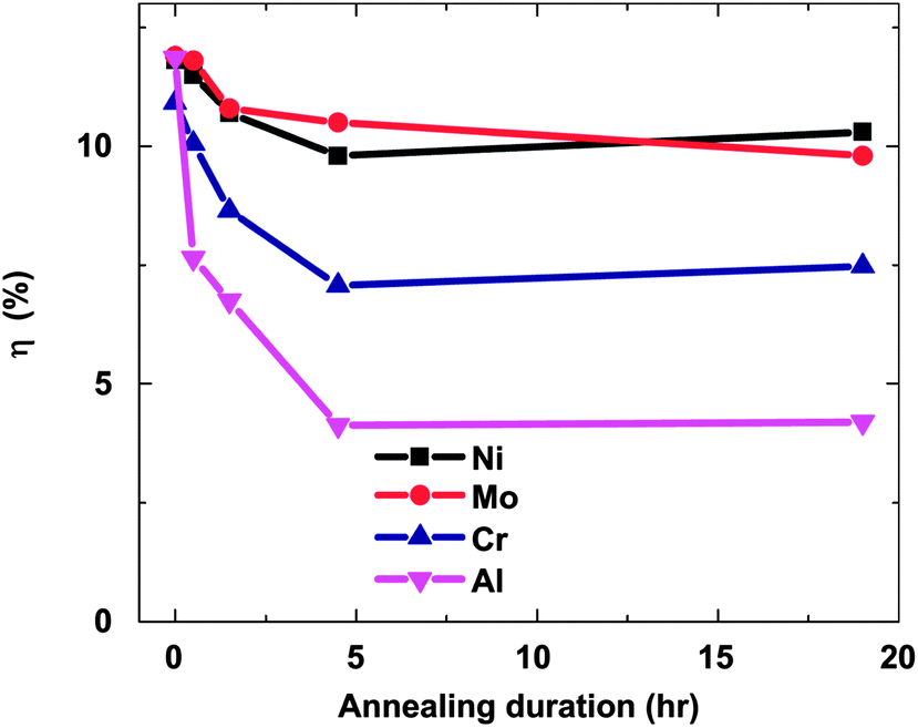 | ||
| Fig. 38 Degradation of cells with different back contacts under vacuum annealing at 200 °C for 4.5 h (reprinted with permission from ref. 473; copyright @ 2012 Elsevier). | ||
6.9 Bifacial solar cells
Bifacial solar cells (ITO/CdTe/CdS/FTO/glass) displayed 7.9 and 1% efficiency for front and rear side illumination respectively. The lower efficiency for back illumination, was due to poor charge carrier collection that were photogenerated far away from heterojunction. In addition, this device was stable compared to standard solar cells with an Cu/Au back contact that were otherwise susceptible to degradation.476 The reduction in the thickness of CdTe to 2.5 μm showed an efficiency of 10.3 and 2.1% for front and back illumination, respectively. The efficiency at back illumination increased to 3.2% and reduced to 8% for the front side with a further decrease in CdTe thickness to 1.0 μm.237 The glass/SnO2:F/CdS/0.68 μm thick CdTe/ZnTe:N/ITO device exhibits efficiencies of 5.7 and 5% for glass and contact side illumination, respectively.477 The QE with glass and contact side illumination showed a higher response at 600 and 800 nm, respectively, which was explained by the wavelength dependence of absorption coefficient, illumination side and position of the junction. For the QE curve with glass side illumination, light must pass through glass, SnO2:F and CdS inducing optical losses at 400–500 nm due to CdS absorption. However, light will first pass through ITO and then to ZnTe:N (2.2 eV) without any QE onset at 560 nm or below for contact side illumination. Thus, it can be assumed that generation and collection of the charge carrier pair takes place from this layer, which induces higher QE compared to glass side illumination at lower wavelength. Since most of photons are absorbed near the back contact far away from the junction, assisted by a weak electric field region, these carriers are more sensitive to back surface recombination.477 The I–V characteristics recorded upon illumination of the front side for glass/SnO2:F/CdS/CdTe/Cu/ITO varied insignificantly for all 8 years of testing compared to starting state. However, Isc was increased by a factor of 2 and additional inflection point appeared in I–V studies compared to the starting state for rear side illumination.478 This difference was accounted for, by the degradation process taking place at the back contact as Cu diffuses over the GBs and shunts the rear barrier due to an increase in the conductivity of GBs. This process decreases the Rs, the main contribution of which was made by a weakly illuminated depletion region of the rear barrier. In this case, shunting of the rear barrier also leads to an increase in its diode saturation current causing inflection points in the I–V curve when illuminated from the rear side.478 These bifacial photovoltaics are attractive for tandem solar cells and its configuration is beneficial for industrial in-line production and also suitable for roll-to-roll manufacturing of solar modules.7. Effects of preparative methods on device performance
The efficiency in the device was governed by the S/Cd ratio in CdS preparation by the CBD method.479 A maximum efficiency of 12.3% was observed for S (thiourea)/Cd (CdCl2) ratio of 5.0 compared with other S/Cd ratio of 1, 2.5 and 10 whose efficiencies were 7.1, 8.3 and 5.4% respectively. The QE reached a maximum for S/Cd = 5 at the lower wavelength region due to the formation of CdTe1−xSx alloy (Fig. 39), while it was not changed in the longer wavelength region. The PL studies revealed that for a S/Cd ratio <5, sulfur goes into the CdS GBs, while the amount of interstitial S decreases due to sulfur precipitation into the solution for a S/Cd ratio >5. Hence, CdS deposition with varied S/Cd content affects the interface characteristics between CdS and CdTe as well as the absorption coefficient of CdS without modifying the bulk properties of CdTe. The cell degradation decreased from 70 to 17% with change in the S/Cd ratio from 3:1 to 7:1.480 The maximum degradation (80%) was observed for an S/Cd ratio of 8:1 and the best efficiency was achieved for an S/Cd ratio of 5:1 (and 6:1). The J–V curve did not show any saturation effect for a fresh device, which is an indication of an acceptable Rs for the device. This cell was kept in an open environment for a period of 36 months. The decrease in efficiency was related to oxidation or chemical changes at the surface leading to changes in shunt resistance together with Cu segregation through the grain boundary of CdS and CdTe (Table 13).480 The efficiency was reduced to 11.2 and 6.3% for CdS grown by CSVT,481,482 due to the larger Rs for CSVT-CdS compared to CBD-CdS solar cells. It was shown that sulfur enrichment in the CBD-CdS layer reduces carrier density at GBs.482 Thus, larger photoconductivity of the CBD-CdS layer may result in better FF. The spectral response indicated an efficient interface between CBD-CdS and CdTe compared to CSVT-CdS and CdTe, though Jsc is almost same for both the solar cells.481 Using photoacoustic spectroscopy, it was shown that the charge carrier recombination velocity is 2.0 ± 0.3 × 103 cm s−1 at the CdS–CdTe interface for this optimum concentration (S/Cd = 5)482 indicating a low density of recombination carriers are available at the interface. In addition, the properties of the CdS layer are correlated with the kinetics of the deposition process with change in thiourea concentration; a low thiourea concentration causes very slow growth leading to a thinner but more homogeneous layer with optimum characteristics. For higher concentrations (S/Cd = 6), the reaction rate becomes progressively large enough to promote quick CdS precipitation resulting in the formation of agglomerates in the solution rather than nucleation on the substrate surface affecting the interface characteristics.482,483 The CBD-CdS showed following characteristics with increase in S/Cd ratio: (i) optical transmittance above threshold increased from 68–72%; (ii) high resistivity in the dark but with a large photoconductive gain; (iii) grain size becomes smaller from 55.4–47.2 nm;483 (iv) diode factor decreased from 2.9–2.1; (v) band gap values increased from 2.45–2.52 eV. The higher band gap improves the Isc, while the small grain size will have fewer pinholes. All these properties account for enhancement in the solar cell performance.479–484 The unique advantage of the CBD technique for depositing CdS is that very thin films (60–80 nm) can be deposited with a uniform surface coverage and low pinhole density. In addition, an absorption coefficient of CBD-CdS will be lower compared to films deposited by other methods having the same thickness.60 In contrast to the above results, efficiency with CBD-CdS layers (150 nm) was as low as 5–6% compared to HVE-CdS layers (300 nm) of 12.3%.397 The surface texture remained smooth before and after vacuum annealing for CBD-CdS and changed from rough to smooth for HVE-CdS. The junction activation step reduced the efficiency from 12.3 to 11.2% due to excess intermixing of CdTe and CdS, as evidenced by a large decrease of the CdTe lattice parameter from 6.499 to 6.446 Å after CdCl2 treatment.397 In another study, a device with CSS-CdS showed a high efficiency (9.63%) compared to CBD-CdS (8.24%).59 The XPS analysis indicated that the Fermi level of the CSS-CdS film is closer to the CB than that of CBD-CdS. The increased n-doping of the CdS layer leads to a higher position of the Fermi level, which results in sufficient band bending at the CdTe side. Thus, the built-in potential of the CdTe film was increased and a higher Voc was obtained. In addition, higher n-doping of the window layer can extend the depletion width in the CdTe layer increasing the photocurrent collection. The other reasons were the better crystallinity, higher optical transmittance and less recombination near the interface between CdTe and CSS-CdS.59
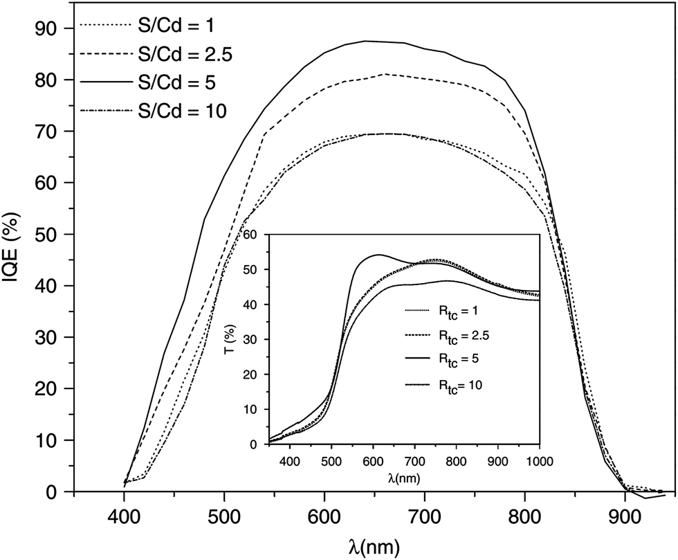 | ||
| Fig. 39 Internal quantum efficiencies for CdTe/CdS solar cells with different thiourea/CdCl2 (Rtc) ratios in the CBD-CdS (reprinted with permission from ref. 479; copyright @ 2006 Elsevier). | ||
| S/Cd | V oc/mV | J sc/mA cm−2 | FF (%) | η (%) | Degradation |
|---|---|---|---|---|---|
| 3:1 |
0.613–0.528 | 18.7–10.2 | 0.58–0.33 | 6.7–1.9 | 70 |
| 4:1 |
0.74–0.623 | 18.7–10.9 | 0.70–0.62 | 9.8–4.3 | 55 |
| 5:1 |
0.745–0.649 | 21.4–17.0 | 0.70–0.46 | 11.1–5.4 | 51 |
| 6:1 |
0.746–0.64 | 20.2–16.4 | 0.73–0.57 | 11.1–6.0 | 44 |
| 7:1 |
0.73–0.649 | 18.4–17.6 | 0.62–0.60 | 8.4–7.0 | 17 |
| 8:1 |
0.524–0.450 | 18.4–5.7 | 0.57–0.41 | 5.5–1.1 | 80 |
The CdTe deposited by MOCVD under a Te-rich ambient resulted in 11.9% efficiency, while those fabricated under Cd-rich conditions were <6% only.140 The monotonic increase of Voc while going from a Cd-rich to Te-rich ambient suggests the improvement in interface quality as a result of atomic interdiffusion, which was beneficial for reducing the lattice mismatch or gradual transition of CdS to CdTe with fewer interface states. Carrier transport analysis showed that transport mechanism switches from tunneling/interface recombination in Cd-rich cells to depletion region recombination limited transport in Te-rich cells.140 Based on XPS, SIMS and optical reflectance measurements, it was concluded that high efficiency devices possess a Te-rich CdTe surface (Cd/Te ratio < 1 or 0.85) with smooth interfaces, while low efficiency cells displayed near stoichiometric or Cd-rich CdTe surfaces and abrupt interfaces (Cd/Te ratio >1).286 The well-defined interference fringes due to abrupt interfaces result in multiple reflections from parallel CdTe layers for low efficiency devices, while such interference fringes were completely absent for high efficiency cells. Since the reflectance coefficient R = [(n2 − n1)/(n2 + n1)]2 at the abrupt interface between the two materials, gradual variation between CdS–CdTe and SnO2–CdS leads to a gradual variation of the refractive index from SnO2 to CdS and CdS to CdTe, which could decrease the reflectance loss as light passes through the glass–SnO2–CdS–CdTe layers and increases the solar cell efficiency. The decrease of optical loss due to gradual change in refractive index is a dominant factor that improved the efficiency in these PV devices.286
8. Effects of particle irradiation on device efficiency
One of the important requirements of solar cells for possible space or satellite applications is the stability against high energy particle irradiation, which is incident on the device material, creates dislocations, displaces atoms from their lattice sites, and introduces electronic traps within the band gap. This reduces carrier concentration, mobility and lifetime leading to a gradual deterioration in performance over a period of time.485,486The effect of 8 MeV electron irradiation of solar cells exhibits different behavior depending on doses ranging from 0.1 to 100 kGy at RT.487 At a very small dose of 0.1 kGy, an enhancement in efficiency was observed due to an increase in minority carrier lifetime in the base region caused by the passivation of recombination centers.488 Above 0.1 kGy, the efficiency was reduced without much change in FF and Voc. Optical absorbance studies revealed that the solar cells turned brown after irradiation and this darkening increased with electron dose up to 25 kGy, beyond which darkening did not change much with dose. This darkening process was due to ionization followed by the creation of color centers in the glass by 8 MeV electrons.487 Batzner et al.489 and Romeo et al.490 have reported similar results for solar cells on glass substrates irradiated with electrons of 1–3 MeV and protons of 5–15 MeV. Thus, irradiation also induces ionization damage in the glass giving rise to color centers enabling photon absorption in the glass itself causing the additional optical loss. Hence, it can be concluded that a low efficiency of superstrate devices upon irradiation may also be due to darkening of the glass and not necessarily associated with device degradation.487 Both the diode ideality factor and reverse saturation current increased above 10 kGy electron dose, indicating the stability against electron irradiation (Fig. 40). The Rs decreased up to 10 kGy and drastically increased thereafter. The cell degradation above 10 kGy was ascribed to decrease in minority carrier diffusion length as a result of radiation-induced defects. There was a marginal difference in the decrease of capacitance for unirradiated (26.7–9.13 nF) and irradiated (26.7–8.65 nF) samples with the frequency at 1 V suggesting that irradiation did not significantly contribute to the concentration of deep level defects at the interface.486,487 For the solar cells developed at ETH Zurich, protons of 650 keV were most damaging, and less damage resulted from 1 and 2.2 MeV protons (Fig. 41), which is in accordance with NIEL estimates (for protons, NIEL is higher for lower energies).116 Proton irradiation has no effect on the efficiencies for low fluencies up to 1011 cm−2. The efficiencies are lost followed by a decrease in Jsc at higher fluencies because of increased recombination density. In contrast, degradation was weakly affected by electron irradiation.116 The use of space quality CeO2 doped glass, which remains transparent even after irradiation, would be beneficial to overcome this problem.
 | ||
| Fig. 40 Reverse saturation current and ideality factor of CdTe/CdS solar cell as functions of electron irradiation dose (reprinted with permission from ref. 487; copyright @ 2009 Elsevier). | ||
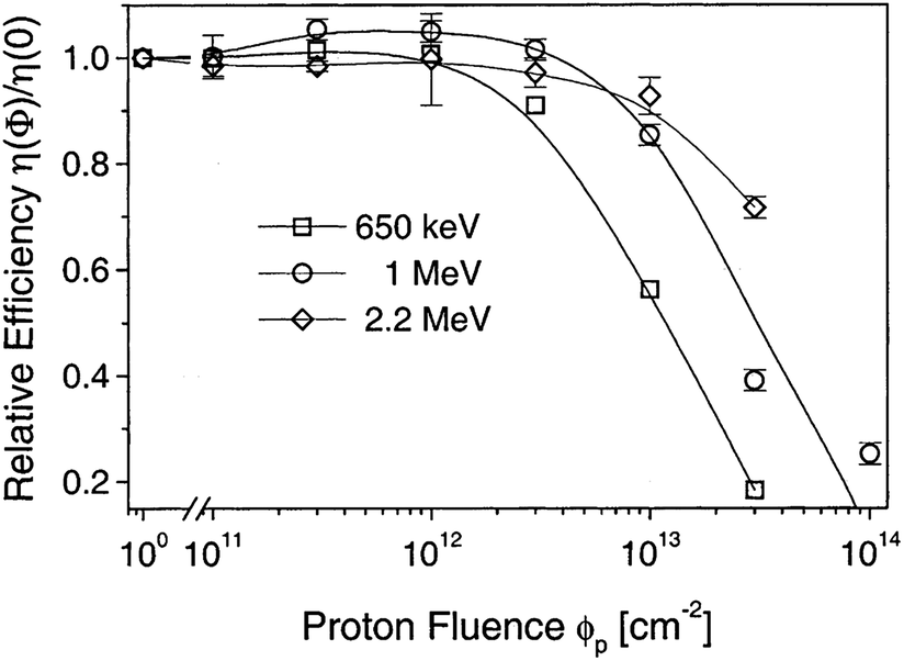 | ||
| Fig. 41 Relative efficiencies of the irradiated CdTe cells as a function of the proton fluence (reprinted with permission from ref. 116; copyright @ 2004 Elsevier). | ||
9. Innovative cell structure
The inverted p–n junction between n-CdTe/p-diamond exhibits an internal QE of 70% at 500 nm (ignoring the reflection and absorption losses of the diamond film). The junction formation between diamond/CdTe results in interface states and dislocations disturbing the photocurrent to some degree.491 The n-CdTe/p-diamond film showed a built-in voltage of 1.0 eV at the junction, comparable to a CdTe/CdS solar cell. The J–V characteristics in the dark behave like a rectifying diode with an ideality factor of 1.23 at 0.1 V. Under illumination, the device produced a Voc, Jsc and FF of 0.23 V, 1.54 mA cm−2 and 0.32, respectively. The external QE measured was 10% for green light at 500 nm and reduced to zero at the absorption edge of 840 nm, indicating a high degree of recombination in the CdTe bulk and low transmittance of the diamond film (Fig. 42).491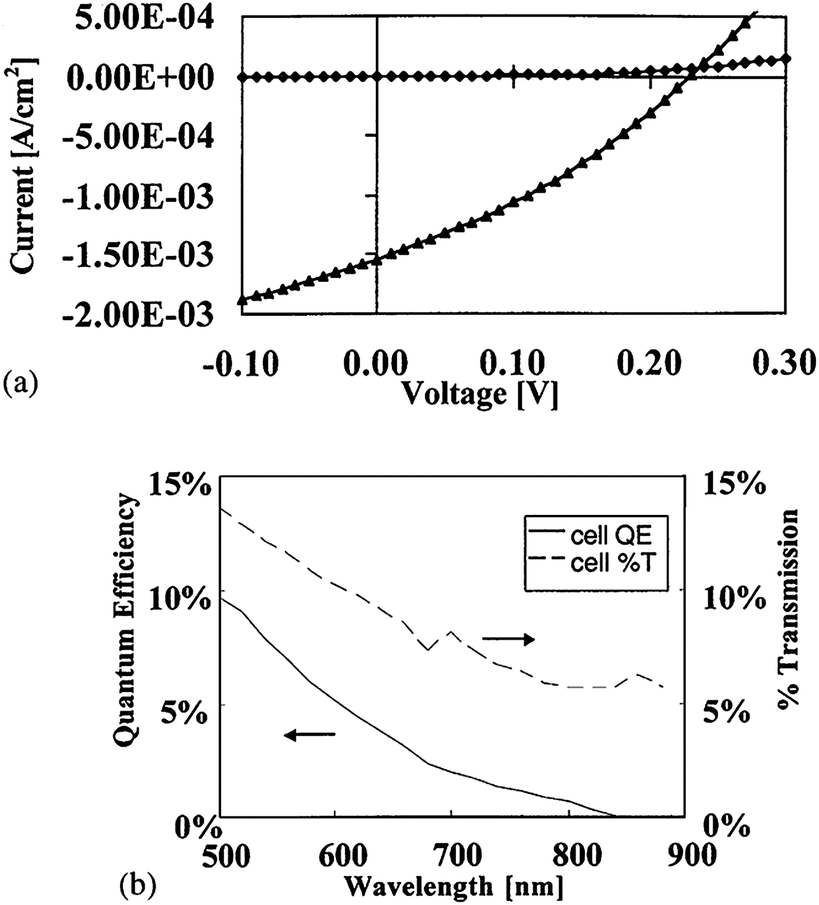 | ||
| Fig. 42 (a) J–V data for the p-diamond/n-CdTe inverted heterojunction solar cell in the dark and under illumination. (b) Spectral response of the diamond/CdTe solar cell (reprinted with permission from ref. 491; copyright @ 2001 Elsevier). | ||
Coating of FCA on a solar cell makes it sensitive to light at wavelengths <510 nm and transforms the wavelength of incident light from the non-incentive (<510 nm) to the incentive region (>510 nm).492 The hemispherical reflectivity of an FCA coated solar cell increased in the wavelength region of 400–500 nm, attributed to the increase of scattering as a result of isotropic emission of fluorescent light. The maximum output power increases to 8 and 14% upon illumination with white light and daylight fluorescent lamps, respectively. This difference is because the light energy at wavelengths <510 nm is larger in the latter case compared to the former. Although FCA did not degrade the cell, it is unsuitable for practical purposes.492 The PV conversion efficiency was increased by 5% for the solar cell with KMgF3:Sm (0.8 mol%).493 This PV composite resulted in a spectral response in the short wavelength region <500 nm due to the broad and strong f–d transition bands in KMgF3:Sm. It was emphasized that thin disc crystal of KMgF3:Sm placed on top of CdTe/CdS did not effect FF and Voc, because the wavelength conversion changes only the distribution of incident photon flux to connect directly with the generation of carrier densities and results in Isc enhancement without changing the diode properties.493
To improve the performance further, device fabrication involving nanostructure materials based on nanopillars, nanowires, nanotubes and nanorods are explored. The solar cell with quantum confinements in both window and absorber layer showed a Voc and Jsc of 112 mV and 10 nA cm−2 for a light density of 2.22 mW cm−2.494 Interestingly, Jsc showed a gradual increase with an increment in light intensity from 2.22–6.6 mW cm−2 without change in Voc. The low efficiency of this solar cell was attributed to intrinsic defects in CdS nanoparticles, as evidenced by both PL and Raman studies. Also, the large surface area of small nanoparticles resulted in substantial diffusion of Te from CdTe to CdS, affecting the junction properties. A new innovative structure with a single crystalline 3D n-CdS nano pillar embedded in polycrystalline p-CdTe exhibits a Voc of 0.62 V and 6% efficiency without the use of antireflective coating or concentrators.495 The conversion efficiency monotonically increased with CdS nanopillar length (H). Interestingly, an efficiency of 0.4% was observed for H = 0. In such a case, only the top surface of CdS nanopillars will be in contact with the CdTe film and hence the small space charge region is obtained with a low carrier collection efficiency. Most of the carriers recombine in the CdTe film via non-radiative pathway at defect-rich GBs. By increasing H (640 nm), the space charge region is effectively increased with improved carrier collection efficiency. The deposited Au/Cu thin layer has a very low transparency (50%), which resulted in major optical losses and low performance.495 The application of CdS nanowires (CNW) embedded in an anodic aluminium oxide-AAO (device A) exhibited an efficiency of 6.5%, whereas the device fabricated only with CNW (device B) had 5.1%.496 For the device A, Jsc and Voc marginally decreased with change in nanowire length from 200–100 nm, while a drastic decline was observed for device B (Fig. 43). The residues and foreign materials present in the gaps between nanowires of device B would cause shunting paths, accounting for its lower efficiency. The presence of AAO will cover the pinholes in CdS preventing the interaction of CdTe with ITO, resulting in low shunting paths. This novel device has following features: (i) the optical absorption edge of CNW lies at 480 nm instead of 512 nm (bulk CdS), which enhances the number of solar photons incident on CdTe absorption layer and increases the light generated current; (ii) CNW are embedded in insulating AAO with much a higher optical transmittance and enable CdTe to absorb more photons (the calculations revealed that 17% improvement in Jsc could be expected); (iii) CdS forms a junction with CdTe only at the top end of CNW. Thus the interface junction area will be typically small resulting in small I0 and large Voc.496 Though the efficiency for reported nanostructured devices are smaller than traditional solar cell designs, they are expected to surpass the Shockley limit when the technology matures and the physics behind the size quantization effects becomes more clear and deeper. The 3D configuration of the window layer can relax the materials requirements in terms of quality and purity, further lowering the costs. However, such materials cost reduction is partially offset by the device fabrication costs, including the anodisation steps and top contact formation.495
 | ||
| Fig. 43 Change in Voc and Jsc for device A and B, as a function of nanowire length (reprinted with permission from ref. 496; copyright @ 2011 IOP Science). | ||
10. Conclusion and future prospects
Due to the small quantities of materials required for their fabrication and their versatility to tune the desired properties of each layer, polycrystalline thin film p-CdTe/n-CdS heterojunction solar cells have become one of the promising contenders for industrial production. The efficiencies in a wide range of 6–20% are achieved with several strategies, such as varying the absorber/window layer thickness, doping the heteroatoms, different preparative methods, different front/back contacts, application of buffer layer and nanostructures, etc. (Table 14). In addition, a junction activation step with hazardous CdCl2 is eliminated using non toxic Freon gas, making this heterostructure more environmentally benign.| Year | η (%) | Significant feature of CdTe/CdS solar cells | Ref. |
|---|---|---|---|
| 1988 | 10.5 | CdS surface was in situ cleaned which minimized the interface states | 250 |
| 1993 & 1994 | 15.8 | CdTe was deposited on CdS by CSS and doped graphite paste was used for ohmic contact | 406, 407 |
| 1996 | 10 | The efficiency was improved after CdCl2 treatment | 375 |
| 1996 | 11.9 | CdTe was deposited by MOVCD under Te-rich ambient | 140 |
| 1997 | 15.4 | Two step CdS formation was used with corning glass as substrate | 426 |
| 1999 | 5.3 | Mo foil was used as substrate | 189 |
| 1999 | 8.9 & 10.6 | CdTe was deposited via a low and high temperature CSS method, respectively | 343 |
| 1999 | 14.6 | Sb2Te3/Mo was used as back contact | 274 |
| 2000 | 10.0 | No antireflection coating, and CdS/Cd1−xZnxS was used as window layer | 102 |
| 2001 | >10.0 | NiTe2 was used as back contact | 466 |
| 2001 | 10.5 | Large surface area of 1376 cm2 thin film solar cell sub module | 458 |
| 8.4 | Aperture area 5413 cm2 | ||
| 2001 | 12.3 | CdS window layer was grown using HVE technique | 397 |
| 2001 | 14.1 | CdTe was deposited via CSS at 630 °C and CdCl2 treatment was carried at 415 °C | 351 |
| 2002 | 18 | Both absorber and window layer were n-type | 409 |
| 2003 | 7.4 | Junction activation step with CdCl2 was more effective than CsCl and MnCl2 | 404 |
| 2003 | 11.0 | Graphite carbon paste with 7 wt% carbon black powder was used for ohmic contact | 459 |
| 2003 | 11.7 | 60 nm Cu2Te back contact was annealed at 180 °C to produce maximum efficiency | 451 |
| 2003 | 12.0 | CdS with optimal thickness of 85 nm was deposited by MOCVD | 271 |
| 2003 | 12.0 | Iodine doped CdTe was used as absorber layer | 446 |
| 2003 | 14.0 | 0.4 μm of fluorine doped In2O3 was used as TCO | 424 |
| 2004 | 7.06 | Substrate was Mo foil with ZnTe:N as back contact | 418 |
| 2004 | 8.3 | Absorber layer Cd1−xZnxTe was electrodeposited with SbCl3 bath | 249 |
| 2004 | 14.0 | Radio frequency sputtered AZO was used as transparent front contact | 419 |
| 2004 | 15.9–16.5 | CdS:O was used as window layer and ZnSnOx was used as buffer layer | 256 |
| 2005 | 11.0 | 2 nm dry Cu was used as back contact | 228 |
| 2005 | 11.2 | CdS window layer was grown by CSVT with growth time being 140 s | 481 |
| 2005 | 14.0 | Oxygen was doped into CdTe layer and ITO:F/SnO2 bilayer front electrode and Mo/Sb2Te3 back contact | 444 |
| 2006 | 11.2 | Ultrathin CdTe (0.7 μm) obtained by magnetron sputtering was used as absorber layer | 120 |
| 2006 | 12.3 | S/Cd ratio was 5 in CdS bath solution grown by CBD | 479 |
| 2006 | 12.5 | Back contact was Ag deposited on Cu-graphite layer | 457 |
| 2007 | 5.7 & 5.0 | Ultrathin bifacial solar cells for glass and contact side illumination respectively | 477 |
| 2007 | 7.4 | CdCl2 was deposited using MOCVD technique for the first time | 303 |
| 2007 | 8.0 | Bi (4 × 1017 cm−3) was doped inside the CdTe matrix | 448 |
| 2007 | 10.3 | Bifacial solar cells: front side illumination with ∼2.5 μm thick CdTe performed better compared to solar cell with CdTe ∼1.0 μm thickness | 237 |
| 2007 | 12.9 | Cu thickness of 10 nm was used as back contact | 455 |
| 2007 | 20.0 | Ultrathin CdTe (<3 μm) was used with ZnTe as back surface field | 253 |
| 2008 | 6.55 | CBD-CdS bilayers (120 + 40 nm) followed by CdCl2 treatment was used as window layer | 427 |
| 2008 | 9.7 | 5 nm Cu thickness of Cu was used as back contact | 452 |
| 2008 | 14.8 | Junction activation was carried with HCF2Cl gas | 393 |
| 2009 | 6.0 | CdS nanopillars was used as window layer | 495 |
| 2009 | 6.3 & 7.03 | Inx(OOH, Sx)y/CdS double layer was used as window layer, with CdS thickness of 100 and 80 nm respectively | 434 |
| 2009 | 11.42 | Cd0.9Zn0.1S was used as window layer | 429 |
| 2010 | 11.0 | Mixture of nitric and acetic acid was used as etchants with Au back contact | 173 |
| 2010 | 11.3 | CSS-CdTe thickness was 5.63 μm | 138 |
| 2010 | 12.2 | MoOx (40 nm)/Ni was used as back contact | 470 |
| 2010 | >15.0 | 1 μm CdTe, 50 nm CdS, 100 nm ZnO buffer layer and 100 nm of BSR (ZnTe or Sb2Te3) was used in the cell structure | 468 |
| 2011 | 4.17 | Graphene front contact with ZnO was used as barrier layer | 423 |
| 2011 | 6.5 | CdS nanowires was used as window layer | 496 |
| 2011 | 7.86 | Boron doped graphene was used as back contact | 460 |
| 2011 | 9.1 | Cu particle doped 3D graphene was used as back contact | 464 |
| 2011 | 9.63 | CSS-CdS solar cells showed higher efficiency compared to CBD-CdS solar cells | 59 |
| 2011 | 10.1 | Bilayer CdS-bottom layer CSS-CdS and top layer CBD-CdS with ∼80 nm total thickness was used as window layer | 59 |
| 2011 | 11.4 | Cu/Mo back contact with ZnO buffer layer was used | 454 |
| 2011 | 11.5 | Cells treated and calcined with dry CdCl2 showed superior performance compared to wet CdCl2 treatment | 319 |
| 2011 | 12.0 | Both CdS and CdTe was fabricated by low temperature CSS method | 395 |
| 2011 | 13.1 | Sb2Te3/Au was used as back contact | 467 |
| 2011 | 15.6 &15.4 | AZO/i:ZnO layer was used as front contact with aluminosilicate and borosilicate glass substrates respectively | 421 |
| 2012 | 6.6 | CBD-CdS films were annealed in the presence of oxygen for 5 minutes prior to CdTe deposition | 60 |
| 2012 | 6.8 | Ultrathin CdTe (1.0 μm) was used as absorber layer and Cd1−xZnxS as window layer | 121 |
| 2012 | 8.3 & 9.9 | SiO2 was used as barrier layer for sodium diffusion and CdCl2 was carried at 350 and 400 °C respectively | 243 |
| 2012 | 12.1 | 1D Cu nanowire/3D graphene was used as back contact | 465 |
| 2012 | 11.5–12.9 | MoOx/M (M = Ni, Mo, Cr, Al and Mg) was used as back contacts | 473 |
| 2012 | 12.0 | Cu2Te/Au back contact was used. | 367 |
| 2012 | 12.1 | Sprayed AZO was used as front contact | 422 |
| 2012 | 14.0 | Both CdS and CdTe were deposited by HVE at 165 and 350 °C, respectively | 128 |
| 2012 | 14.0–14.6 | Junction activation was carried with HCF2Cl gas and CdS was treated in oxygen atmosphere before CdTe deposition | 392 |
| 2013 | 13.6 | The copper was doped into CdTe matrix, in substrate configuration | 416b |
Increasing the efficiency, reliability and life time of this device has been a focal point from two decades and yet the best efficiencies achieved to date are still far from the theoretical limit. Together with technological problems, progress towards improvement is suppressed by the lack of scientific knowledge about the processes occurring at various interfaces of the device. Inevitably, a number of interfaces between materials with different crystal structures and/or lattice constants cause complexity in device formation. The various failure mechanisms can be active simultaneously, making their identification and rectification difficult. As a result, fabrication processes are slowly approaching their limits and this is the main reason for only marginal improvement, despite the intensive efforts for the last two decades.
The reason for such slow progress appears to be lack of understanding of critical issues like: junction activation treatment, which changes the bulk, interfacial and grain boundary properties; the formation of stable back contacts; and impurities diffusion within the device. This complexity arises due to the influence of multiple parameters like: layer thickness; grain size; donor/acceptor profile; carrier generation rate; recombination dynamics at various interfaces; CdS–CdTe intermixing; quasi Fermi level distribution; band alignments among the interfaces; diffusivity of metal from the back contact; influence of barrier layer, if any; induced chemical reactions during processing, etc., on the solar cell performance. In addition, both CdS and CdTe are polycrystalline and hence their properties vary depending on precursor chemistry, growth conditions, technique and annealing ambient. Due to the difficulty of performing scientific study on randomly oriented polycrystalline thin films, massive research has utilized a semi-empirical approach that has hampered the advancement of fundamental understanding. From the literature, it can be concluded that device performance cannot be described by taking the properties of the component materials in their bulk form and applying junction theory.
Despite the intensified research, there is no rule of thumb for better performance, and reported mechanisms are often beyond intuition. As suggested by Kosyachenko et al.,497 resistivity, absorber layer thickness, non-compensated acceptor concentration and carrier lifetime should be ∼0.1 Ω cm, ≥20–30 μm, ≥1016 cm−3 and ≥10−6 s, respectively, to achieve a theoretical efficiency of ∼30%. In practice, an electrical barrier within the multilayer leads to efficiency loss. The limited conclusive information about the understanding of important relationships between the processing conditions and device characteristics further complicates the development of this novel device. Hence, systematic research is necessary to understand the apparent complexities in the cell structure and new innovative technologies and concepts are essential to solve the persistent challenges of CdTe/CdS photovoltaics.
Abbreviations
| AZO | Aluminium doped ZnO |
| ALE | Atomic layer epitaxy |
| APCVD | Atomic pressure chemical vapor deposition |
| APCSS | Atmospheric pressure close space sublimation |
| BSR | Back surface reflector |
| CB | Conduction band |
| CSS | Close-space sublimation |
| CSVT | Close-space vapor transport |
| DLTS | Deep level transient spectroscopy |
| DFT | Density functional theory |
| GBs | Grain boundaries |
| ED | Electrodeposition |
| ECU | European currency unit |
| FF | Fill factor |
| FCA | Fluorescent coloring agent |
| HVE | High vacuum evaporation |
| IPCE | Incident photon to conversion efficiency |
| ITO | Indium tin oxide |
| i:ZnO | Intrinsic ZnO |
| LBIC | Light beam induced current |
| MBE | Molecular beam epitaxy |
| MOVCD | Metallorganic vapor chemical deposition |
| NIEL | Non ionization energy loss |
| V oc | Open circuit voltage |
| PV | Photovoltaic |
| PL | Photoluminescence |
| QE | Quantum efficiency |
| R s | Series resistance |
| I sc | Short circuit current |
| J sc | Short circuit current density |
| SIMS | Secondary ion mass spectroscopy |
| TCO | Transparent conducting oxide |
| VB | Valence band |
| VBM | Valence band maximum |
| VCd | Vacancies in cadmium or cadmium vacancies |
| XPS | X-Ray photoelectroscopy |
Acknowledgements
One of the authors Dr S. Girish Kumar acknowledges financial support from the Dr Daulat Singh Kothari Post Doctoral Fellowship Cell and the Department of Physics, IISc, Bangalore for providing the research facilities.References
- P. V. Kamat, J. Phys. Chem. C, 2008, 112, 18737–18753 CAS.
- T. L. Chu and S. S. Chu, Solid-State Electron., 1995, 38, 533–549 CrossRef CAS.
- A. D. Compaan, Sol. Energy Mater. Sol. Cells, 2006, 90, 2170–2180 CrossRef CAS PubMed.
- V. Avrutin, N. Izyumskaya and H. Morkoc, Superlattices Microstruct., 2011, 49, 337–364 CrossRef CAS PubMed.
- M. Afzaal and P. O. Brien, J. Mater. Chem., 2006, 16, 1597–1602 RSC.
- J. A. Chang, J. H. Rhee, S. H. Im, Y. H. Lee, H. J. Kim, S. I. Seok, M. K. Nazeeruddin and M. Gratzel, Nano Lett., 2010, 10, 2609–2612 CrossRef CAS PubMed.
- Y. Chiba, A. Islam, Y. Watanabe, R. Komiya, N. Koide and L. Han, Jpn. J. Appl. Phys., 2006, 45, L638–L640 CrossRef CAS.
- S. Gunes, H. Neugebauer and N. S. Sariciftci, Chem. Rev., 2007, 107, 1324–1338 CrossRef PubMed.
- T. M. Clarke and J. R. Durrant, Chem. Rev., 2010, 110, 6737–6767 CrossRef PubMed.
- W. U. Huynh, J. J. Dittmer and A. P. Alivisatos, Science, 2002, 295, 2425–2427 CrossRef CAS PubMed.
- K. W. Johnston, A. G. P. Abraham, J. P. Clifford, S. H. Myrskog, D. D. MacNeil, L. Levina and E. H. Sargent, Appl. Phys. Lett., 2008, 92, 151115 CrossRef.
- A. J. Mozer, Y. Wada, K. J. Jiang, N. Masaki, S. Yanagida and S. N. Mori, Appl. Phys. Lett., 2006, 89, 043509 CrossRef.
- P. V. Kamat, J. Phys. Chem. Lett., 2013, 4, 908–918 CrossRef CAS.
- P. V. Kamat, K. Tvrdy, D. R. Baker and J. G. Radich, Chem. Rev., 2010, 110, 6664–6688 CrossRef CAS PubMed.
- J. Yu, J. Fan and K. Lv, Nanoscale, 2010, 2, 2144–2149 RSC.
- M. D. G. Potter, M. Cousins, K. Durose and D. P. Halliday, J. Mater. Sci., 2000, 11, 525–530 CAS.
- J. Fan, S. Liu and J. Yu, J. Mater. Chem., 2012, 22, 17027–17036 RSC.
- S. Emin, S. P. Singh, L. Han, N. Satoh and A. Islam, Sol. Energy, 2011, 85, 1264–1282 CrossRef CAS PubMed.
- A. Hagfeldt, G. Boschloo, L. Sun, L. Kloo and H. Pettersson, Chem. Rev., 2010, 110, 6595–6663 CrossRef CAS PubMed.
- A. W. Hains, Z. Liang, M. A. Woodhouse and B. A. Gregg, Chem. Rev., 2010, 110, 6689–6735 CrossRef CAS PubMed.
- A. J. Nozik, M. C. Beard, J. M. Luther, M. Law, R. J. Ellingson and J. C. Johnson, Chem. Rev., 2010, 110, 6873–6890 CrossRef CAS PubMed.
- B. O'regan and M. Gratzel, Nature, 1991, 353, 737–740 CrossRef CAS.
- The British Photovoltaic Association, Photovoltaics in the UK: Facing the Challenge, 1999 Search PubMed.
- W. H. Bloss, F. Pfistererr, M. Schubert and T. Walter, Progr. Photovolt.: Res. Appl., 1995, 3, 3–24 CrossRef CAS.
- D. A. Cusano, Solid-State Electron., 1963, 6, 217–218 CrossRef CAS.
- D. Bonnet, Thin Solid Films, 2000, 361–362, 547–552 CrossRef CAS , and references cited therein.
- A. M. Acevedo, Sol. Energy Mater. Sol. Cells, 2006, 90, 678–685 CrossRef PubMed.
- M. I. Dharmadasa, Prog. Cryst. Growth Charact. Mater., 1998, 36, 249–290 CrossRef.
- L. A. Kosyachenko, X. Mathew, V. V. Motushchuk and V. M. Sclyarchuk, Semiconductors, 2005, 39, 539–542 CrossRef CAS.
- M. Woodhouse, A. Goodrich, R. Margolis, T. James, R. Dhere, T. Gessert, T. Barnes, R. Eggert and D. Albin, Sol. Energy Mater. Sol. Cells, 2013, 115, 199–212 CrossRef CAS PubMed.
- O. Savadogo, Sol. Energy Mater. Sol. Cells, 1998, 52, 361–388 CrossRef CAS.
- M. Marwede, W. Berger, M. Schlummer, A. Maurer and A. Rellerr, Renewable Energy, 2013, 55, 220–229 CrossRef CAS PubMed.
- K. Durose, S. E. Asher, W. Jaegermann, D. Levi, B. E. McCandless, W. Metzger, H. Moutinho, P. D. Paulson, C. L. Perkins, J. R. Sites, G. Teeter and Terheggen, Progr. Photovolt.: Res. Appl., 2004, 12, 177–217 CrossRef CAS.
- T. A. Gessert, S. H. Wei, J. Ma, D. S. Albin, R. G. Dhere, J. N. Duenow, D. Kuciauskas, A. Kanevce, T. M. Barnes, J. M. Burst, W. L. Rance, M. O. Reese and H. R. Moutinho, Sol. Energy Mater. Sol. Cells, 2013, 119, 149–155 CrossRef CAS PubMed , accepted.
- D. Bonnet, Int. J. Sol. Energy, 1992, 12, 1–14 CrossRef.
- M. M. Aliyu, M. A. Islam, N. R. Hamzah, M. R. Karim, M. A. Matin, K. Sopian and N. Amin, Int. J. Photoenergy, 2012, 351381 Search PubMed.
- L. A. Kosyachenko, X. Mathew, V. Y. Roshko and E. V. Grushko, Sol. Energy Mater. Sol. Cells, 2013, 114, 179–185 CrossRef CAS PubMed.
- R. W. Birkmire and E. Eser, Annu. Rev. Mater. Sci., 1997, 27, 625–653 CrossRef CAS.
- M. G. Mahesha, K. V. Bangera and G. K. Shivakumar, Mater. Sci. Semicond. Process., 2009, 12, 89–93 CrossRef CAS PubMed.
- M. A. Green, J. Mater. Sci.: Mater. Electron., 2007, 18, S15–S19 CrossRef CAS PubMed.
- J. Versluys, P. Clauws, P. Nollet, S. Degrave and M. Burgelman, Thin Solid Films, 2003, 431–432, 148–152 CrossRef CAS.
- P. N. Gibson, M. A. Baker, E. D. Dunlop, M. E. Ozsan, D. Lincot, M. Froment and G. Agostinelli, Thin Solid Films, 2001, 387, 92–96 CrossRef CAS.
- H. A. Mohamed, J. Appl. Phys., 2013, 113, 093105 CrossRef.
- A. Bosio, N. Romeo, S. Mazzamuto and V. Canevari, Prog. Cryst. Growth Charact. Mater., 2006, 52, 247–279 CrossRef CAS PubMed.
- T. M. Razykov, C. S. Ferekides, D. Morel, E. Stefanakos, H. S. Ullal and H. M. Upadhyaya, Sol. Energy, 2011, 85, 1580–1608 CrossRef CAS PubMed.
- A. Bosio, A. Romeo, D. Menossi, S. Mazzamuto and N. Romeo, Cryst. Res. Technol., 2011, 46, 857–864 CrossRef CAS.
- I. M. Dharmadasa, Curr. Appl. Phys., 2009, 9, e2–e6 CrossRef PubMed.
- M. A. Green, K. Emery, Y. Hishikawa, W. Warta and E. D. Dunlop, Prog. Photovoltaics, 2013, 21, 1–11 Search PubMed.
- I. M. Dharmadasa, J. D. Bunning, A. P. Samantilleke and T. Shen, Sol. Energy Mater. Sol. Cells, 2005, 86, 373–384 CrossRef CAS PubMed.
- L. Kranz, S. Buecheler and A. N. Tiwari, Sol. Energy Mater. Sol. Cells, 2013, 119, 278–280 CrossRef CAS PubMed.
- A. Bosio, D. Menossi, S. Mazzamuto and N. Romeo, Thin Solid Films, 2011, 519, 7522–7525 CrossRef CAS PubMed.
- J. Perrenoud, B. Schaffner, S. Buecheler and A. N. Tiwari, Sol. Energy, 2011, 95, S8–S12 CAS.
- S. S. Hegedus and W. N. Shafarman, Progr. Photovolt.: Res. Appl., 2004, 12, 155–176 CrossRef CAS.
- O. Vigil, R. O. Landin, J. Fandino and F. C. Gandarilla, J. Phys. Chem. Solids, 2010, 71, 404–406 CrossRef CAS PubMed.
- T. L. Chu, S. S. Chu, C. Ferekides, C. Q. Wu, J. Britt and C. Wang, J. Appl. Phys., 1991, 70, 7608–7612 CrossRef CAS.
- K. Zweibel, Sol. Energy Mater. Sol. Cells, 2000, 63, 375–386 CrossRef CAS.
- N. Romeo, A. Bosio and A. Romeo, Sol. Energy Mater. Sol. Cells, 2010, 94, 2–7 CrossRef CAS PubMed.
- J. Han, C. Spanheimer, G. Haindl, G. Fu, V. Krishnakumar, J. Schaffner, C. Fan, K. Zhao, A. Klein and W. Jaegermann, Sol. Energy Mater. Sol. Cells, 2011, 95, 816–820 CrossRef CAS PubMed.
- J. Han, C. Wao, T. Jiang, C. Spanheimer, G. Haindl, G. Fu, V. Krishnakumar, K. Zhao, A. Klein and W. Jaegermann, J. Alloys Compd., 2011, 509, 5285–5289 CrossRef CAS PubMed.
- X. Mathew, J. S. Cruz, D. R. Coronado, A. R. Millan, G. C. Segura, E. R. Morales, O. S. Martinez, C. C. Garcia and E. P. Landa, Sol. Energy, 2012, 86, 1023–1028 CrossRef CAS PubMed.
- K. D. Rogers, J. D. Painter, D. W. Lane and M. Heally, J. Electron. Mater., 1999, 28, 112–117 CrossRef CAS.
- D. S. Albin, Y. Yan and M. M. Al-Jassim, Progr. Photovolt.: Res. Appl., 2002, 10, 309–322 CrossRef CAS.
- J. Luschitz, K. L. Wollny, A. Klein and K. W. Jaegermann, Thin Solid Films, 2007, 515, 5814–5818 CrossRef CAS PubMed.
- V. Krishnakumar, J. Han, A. Klein and W. Jaegermann, Thin Solid Films, 2011, 519, 7138–7141 CrossRef CAS PubMed.
- N. Armani, G. Salviati, L. Nasi, N. Bosio, S. Mazzamuto and N. Romeo, Thin Solid Films, 2007, 515, 6184–6187 CrossRef CAS PubMed.
- J. Han, C. Liao, T. Jiang, G. Fu, V. Krishnakumar, C. Spanheimer, G. Haindl, K. Zhao, A. Klein and W. Jaegermann, Mater. Res. Bull., 2011, 46, 194–198 CrossRef CAS PubMed.
- Q. Jiang, A. W. Brinkmann, B. J. Cantwell, J. T. Mullins, F. Dierre, A. Basu, P. Veeramani and P. Selin, J. Electron. Mater., 2009, 38, 1548–1553 CrossRef CAS.
- R. A. Berrigan, N. Maung, S. J. C. Irvine, D. J. C. Hamilton and D. Ellis, J. Cryst. Growth, 1998, 195, 718–724 CrossRef CAS.
- S. J. C Irvine, V. Barrioz, D. Lamb, E. W. Jones and R. L. R. Jones, J. Cryst. Growth, 2008, 310, 5198–5203 CrossRef PubMed.
- G. Zoppi, K. Durose, S. J. C. Irvine and V. Barrioz, Semicond. Sci. Technol., 2006, 21, 763–770 CrossRef CAS.
- S. J. C. Irvine, A. Hartley and A. Stafford, J. Cryst. Growth, 2000, 221, 117–123 CrossRef CAS.
- Y. Y. Proskuryakov, K. Durose, J. D. Major, M. K. A. Turkestani, V. Barrioz, S. J. C. Irvine and E. W. Jones, Sol. Energy Mater. Sol. Cells, 2009, 93, 1572–1581 CrossRef CAS PubMed.
- A. K. Rakhashani, J. Appl. Phys., 2001, 90, 4265–4271 CrossRef.
- S. K. Das and G. C. Morris, Sol. Energy Mater. Sol. Cells, 1993, 28, 305–316 CrossRef CAS.
- N. W. Duffy, D. Lane, M. E. Ozsan, L. M. Peter, K. D. Rogers and R. L. Wang, Thin Solid Films, 2000, 361–362, 314–320 CrossRef CAS.
- N. W. Duffy, L. M. Peter, R. L. Wang, D. W. Lane and K. D. Rogers, Electrochim. Acta, 2000, 45, 3355–3365 CrossRef CAS.
- J. Touskova, K. Kindl and J. Tousek, Thin Solid Films, 1997, 293, 272–276 CrossRef CAS.
- J. M. Hartmann, G. Feuillet, M. Charleux and H. Mariette, J. Appl. Phys., 1996, 79, 3035–3041 CrossRef CAS.
- (a) S. Ikegami, Sol. Cells, 1988, 23, 89–105 CrossRef CAS; (b) B. T. Ahn, B. W. Han and G. Y. Chung, Sol. Energy Mater. Sol. Cells, 1998, 50, 155–161 CrossRef CAS; (c) G. Y. Chung, S. C. Park, K. Cho and B. T. Ahn, J. Appl. Phys., 1995, 78, 5493–5498 CrossRef CAS.
- M. Shao, A. Fischer, D. Grecu, U. Jayamaha, E. Bykov, G. C. Puente, R. G. Bohn and A. D. Compaan, Appl. Phys. Lett., 1996, 69, 3045–3047 CrossRef CAS.
- Y. K. Jun and H. B. Im, J. Electrochem. Soc., 1988, 135, 1658–1661 CrossRef CAS PubMed.
- S. T. Edwards, A. F. Schreiner, T. M. Myers and J. F. Schetzina, J. Appl. Phys., 1983, 54, 6785–6786 CrossRef CAS.
- A. Salavei, I. Rimmaudo, F. Piccinelli and A. Romeo, Thin Solid Films, 2013, 535, 257–260 CrossRef CAS PubMed.
- A. Bosio, N. Romeo, A. Podesta, S. Mazzamuto and V. Canevari, Cryst. Res. Technol., 2005, 40, 1048–1053 CrossRef CAS.
- I. V. Fisher, S. R. Cohen, K. Gartsman, A. Ruzin and D. Cahen, Adv. Funct. Mater., 2006, 16, 649–660 CrossRef.
- M. A. Green, K. Emery, Y. Hishikawa and W. Warta, Progr. Photovolt.: Res. Appl., 2010, 18, 346–352 CrossRef.
- M. A. Green, K. Emery, D. L. King, S. Igari and W. Warta, Progr. Photovolt.: Res. Appl., 2003, 11, 347–352 CrossRef CAS.
- M. A. Green, K. Emery, Y. Hishikawa and W. Warta, Progr. Photovolt.: Res. Appl., 2009, 17, 320–326 CrossRef CAS.
- G. Khrypunov, A. Romeo, F. Kurdesau, D. L. Batzner, H. Zogg and A. N. Tiwari, Sol. Energy Mater. Sol. Cells, 2006, 90, 664–677 CrossRef CAS PubMed.
- R. Scheer, T. Walter, H. W. Schock, M. L. Fearheiley and H. J. Lewerenz, Appl. Phys. Lett., 1993, 63, 3294–3296 CrossRef CAS.
- J. Wallentin, N. Anttu, D. Asoli, M. Huffman, I. Aberg, M. H. Magnusson, G. Siefer, P. F. Kailuweit, F. Dimroth, B. Witzigmann, H. Q. Xu, L. Samuelson, K. Deppert and M. T. Borgstrom, Science, 2013, 339, 1057–1060 CrossRef CAS PubMed.
- L. L. Kazmerski, J. Electron Spectrosc. Relat. Phenom., 2006, 150, 105–135 CrossRef CAS PubMed.
- G. Mariani, A. C. Scofield, C. H. Hung and D. L. Huffaker, Nat. Commun., 2013, 4, 1497 CrossRef PubMed.
- J. J. Loferski, J. Appl. Phys., 1956, 27, 777–784 CrossRef CAS.
- A. M. Acevedo, Sol. Energy Mater. Sol. Cells, 2006, 90, 2213–2220 CrossRef PubMed.
- K. Mitchell, A. L. Fahrenbruch and R. H. Bube, J. Appl. Phys., 1977, 48, 1977–1978 Search PubMed.
- Z. Bai, J. Yang and D. Wang, Appl. Phys. Lett., 2011, 99, 143502 CrossRef.
- P. Capper, Properties of Narrow Gap Cadmium-Based Compounds, EMIS Data Reviews Series, no. 10, INPSEC, Exeter, 1994 Search PubMed.
- K. D. Rogers, J. D. Painter, M. J. Healy, D. W. Lane and M. E. Ozsan, Thin Solid Films, 1999, 339, 299–304 CrossRef CAS.
- Y. Y. Loginov, K. Durose, H. M. Al-Allak, S. A. Galloway, S. Oktik, A. W. Brinkman, H. Richter and D. Bonnet, J. Cryst. Growth, 1996, 161, 159–163 CrossRef CAS.
- A. Romeo, M. Terheggen, D. A. Ras, D. L. Batzner, F. J. Haug, M. Kalin, D. Rudmann and A. N. Tiwari, Progr. Photovolt.: Res. Appl., 2004, 12, 93–111 CrossRef CAS.
- I. O. Oladeji, L. Chow, C. S. Ferekides, V. Viswanathan and Z. Zhao, Sol. Energy Mater. Sol. Cells, 2000, 61, 203–211 CrossRef CAS.
- T. L. Chu, S. S. Chu, C. S. Ferekides, C. Q. Wu, J. Britt and C. Wang, J. Cryst. Growth, 1992, 117, 1073 CrossRef.
- Z. Fang, X. C. Wang, H. C. Wu and C. Z. Zhao, Int. J. Photoenergy, 2011, 297350 Search PubMed.
- P. Hu, B. Li, L. Feng, J. Wu, H. Jiang, H. Yang and X. Xiao, Surf. Coat. Technol., 2012, 213, 84–89 CrossRef CAS PubMed.
- J. R. Sites and X. Liu, Prog. Photovoltaics, 1995, 3, 307–314 CAS.
- K. W. Mitchell, C. Eberspacher, F. Cohen, J. Avery, G. Duran and W. Bottenberg, Sol. Cells, 1988, 23, 49–57 CrossRef.
- F. L. C. Alvarado, J. A. I. Chavez, O. V. Galan, E. S. Meza, E. L. Chavez and G. C. Puente, Thin Solid Films, 2010, 518, 1796–1798 CrossRef PubMed.
- D. W. Niles and H. Hochst, Phys. Rev. B: Condens. Matter, 1990, 41, 12710–12719 CrossRef CAS.
- S. H. Wei, S. B. Zhang and A. Zunger, J. Appl. Phys., 2000, 87, 1304–1311 CrossRef CAS.
- J. Gao, W. Jie, Y. Yuan, G. Zha, L. Xu, H. Wu, Y. Wang, H. Yu and J. Zhu, Chin. Phys. Lett., 2012, 29, 057301 CrossRef.
- P. Boieriu, R. Sporken and S. Sivananthan, J. Vac. Sci. Technol., B, 2002, 20, 1777–1780 CAS.
- J. Fritsche, T. Schulmeyer, D. Kraft, A. Thiben, A. Klein and W. Jaegermann, Appl. Phys. Lett., 2002, 81, 2297–2299 CrossRef CAS.
- K. Nishi, H. Ohyama, T. Suzuki, T. Mitsuyu and T. Tomimasu, Appl. Phys. Lett., 1997, 70, 3585–3587 CrossRef CAS.
- R. W. Miles, K. M. Hynes and I. Forbes, Prog. Cryst. Growth Charact. Mater., 2005, 51, 1–42 CrossRef CAS PubMed.
- D. L. Batzner, A. Romeo, M. Terheggen, M. Dobeli, H. Zogg and A. N. Tiwari, Thin Solid Films, 2004, 451–452, 536–543 CrossRef CAS PubMed.
- I. V. Fisher, K. D. Dobson, J. Nair, E. Bezalel, G. Hodes and D. Cahen, Adv. Funct. Mater., 2003, 13, 289–299 CrossRef.
- L. A. Kosyachenko, E. V. Grushko and X. Mathew, Sol. Energy Mater. Sol. Cells, 2012, 96, 231–237 CrossRef CAS PubMed.
- A. G. Aberle, Thin Solid Films, 2009, 517, 4706–4710 CrossRef CAS PubMed.
- A. Gupta, V. Parikh and A. D. Compaan, Sol. Energy Mater. Sol. Cells, 2006, 90, 2263–2271 CrossRef CAS PubMed.
- A. J. Clayton, S. J. C. Irvine, E. W. Jones, G. Kartopu, V. Barrioz and W. S. M. Brooks, Sol. Energy Mater. Sol. Cells, 2012, 101, 68–72 CrossRef CAS PubMed.
- N. R. Paudel, K. A. Wieland and A. D. Compaan, Sol. Energy Mater. Sol. Cells, 2012, 105, 109–112 CrossRef CAS PubMed.
- V. P. Singh, O. M. Erickson and J. H. Chao, J. Appl. Phys., 1995, 78, 4538–4542 CrossRef CAS.
- K. D. Dobson, I. V. Fisher, G. Hodes and D. Cahen, Adv. Mater., 2001, 13, 1495–1499 CrossRef CAS.
- I. Irfan, H. Lin, W. Xia, H. N. Wu, C. W. Tang and Y. Gao, Sol. Energy Mater. Sol. Cells, 2012, 105, 86–89 CrossRef CAS PubMed.
- M. Terheggen, H. Heinrich, G. Kostorz, D. Baetzner, A. Romeo and A. N. Tiwari, Interface Sci., 2004, 12, 259–266 CrossRef CAS.
- D. S. Boyle, S. Hearne, D. R. Johnson and P. O. Brien, J. Mater. Chem., 1999, 9, 2879–2884 RSC.
- L. Kranz, J. Perrenoud, F. Pianezzi, C. Gretener, P. Rossbach, S. Buecheler and A. N. Tiwari, Sol. Energy Mater. Sol. Cells, 2012, 105, 213–219 CrossRef CAS PubMed.
- F. Molva, J. P. Chamonal and J. L. Pautrat, Phys. Status Solidi B, 1982, 109, 635–644 CrossRef.
- J. Sites and J. Pan, Thin Solid Films, 2007, 515, 6099–6102 CrossRef CAS PubMed.
- A. E. Abken, Sol. Energy Mater. Sol. Cells, 2002, 73, 391–409 CrossRef CAS.
- A. E. Abken and O. J. Bartlet, Thin Solid Films, 2002, 403–404, 216–222 CrossRef CAS.
- J. Y. W. Seto, J. Appl. Phys., 1975, 46, 5247–5254 CrossRef CAS.
- K. Durose, D. Boyle, A. Abken, C. J. Ottley, P. Nollet, S. Degrave, M. Burgelman, R. Wendt, J. Beier and D. Bonnet, Phys. Status Solidi B, 2002, 229, 1055–1064 CrossRef CAS.
- J. R. Sites, J. E. Granata and J. F. Hiltner, Sol. Energy Mater. Sol. Cells, 1998, 55, 43–50 CrossRef CAS.
- T. D. Dzhafarov and M. Caliskan, J. Phys. D: Appl. Phys., 2007, 40, 4003–4009 CrossRef CAS.
- K. Durose, A. J. W. Yates, A. Szczerbakow, J. Domagala, Z. Golacki and K. Swiatek, J. Phys. D: Appl. Phys., 2002, 35, 1997–2007 CrossRef CAS.
- J. D. Major, Y. Y. Proskuryakov, K. Durose, G. Zoppi and I. Forbes, Sol. Energy Mater. Sol. Cells, 2010, 94, 1107–1112 CrossRef CAS PubMed.
- H. Moeller, Semiconductors for Solar Cells, Artech, Boston, MA, 1993 Search PubMed.
- H. C. Chou, A. Rohatgi, N. M. Jokerst, S. Kamra, S. R. Stock, S. L. Lowrie, R. K. Ahrenkiel and D. H. Levi, Mater. Chem. Phys., 1996, 43, 178–182 CrossRef CAS.
- Y. Yan, D. Albin and M. M. Al-Jassim, Appl. Phys. Lett., 2001, 78, 171–173 CrossRef CAS.
- M. Kontges, R. R. Koch, P. Nollet, J. Beier, R. Schaffler and J. Parisi, Thin Solid Films, 2002, 403–404, 280–286 CrossRef CAS.
- D. L. Batzner, G. Agostinelli, A. Romeo, H. Zogg and A. N. Tiwari, Mater. Res. Soc. Symp. Proc, 2001, 668, H5-17 CrossRef PubMed.
- V. P. Singh, D. L. Linman, D. W. Dils, J. C. McClure and G. B. Lush, Sol. Energy Mater. Sol. Cells, 2000, 63, 445–466 CrossRef CAS.
- A. Niemegeers and M. Burgelman, J. Appl. Phys., 1997, 81, 2881–2886 CrossRef CAS.
- T. L. Chu and S. S. Chu, Progr. Photovolt.: Res. Appl., 1993, 1, 31–42 CrossRef CAS.
- C. S. Ferekides, U. Balasubramanian, R. Mamazza, V. Viswanathan, H. Zhao and D. L. Morel, Sol. Energy, 2004, 77, 823–830 CrossRef CAS PubMed.
- J. R. Sites, Sol. Energy Mater. Sol. Cells, 2003, 75, 243–251 CrossRef CAS.
- A. L. Fahrenbruch, Sol. Cells, 1987, 21, 399–412 CrossRef CAS.
- K. Durose, P. R. Edwards and D. P. Halliday, J. Cryst. Growth, 1999, 197, 733–742 CrossRef CAS.
- A. Klein, F. Sauberlich, B. Spath, T. Schulmeyer and D. Kraft, J. Mater. Sci., 2007, 42, 1890–1900 CrossRef CAS.
- C. R. Corwine, A. O. Pudov, M. Gloeckler, S. H. Demtsu and J. R. Sites, Sol. Energy Mater. Sol. Cells, 2004, 82, 481–489 CAS.
- M. Holf and H. Rauschenbach, Adv. Energy Convers., 1963, 3, 455–479 CrossRef.
- Y. Marfaing, Thin Solid Films, 2001, 387, 123–128 CrossRef CAS.
- T. Potlog, L. Ghimpu and C. Antoniuc, Thin Solid Films, 2007, 515, 5824–5827 CrossRef CAS PubMed.
- R. R. King, D. C. Law, K. M. Edmondson, C. M. Fetzer, G. S. Kinsey, H. Yoon, R. A. Sherif and N. H. Karam, Appl. Phys. Lett., 2007, 90, 183516 CrossRef.
- D. L. Batzner, M. E. Oszan, D. Bonnet and K. Bucher, Thin Solid Films, 2000, 361–362, 288–292 CrossRef CAS.
- X. Li, D. W. Niles, F. S. Hasoon, R. J. Matson and P. Sheldon, J. Vac. Sci. Technol., A, 1999, 17, 805–809 CAS.
- D. Goren, G. Asa and G. Nemirovsky, J. Appl. Phys., 1996, 80, 5083–5088 CrossRef CAS.
- D. Rioux, D. W. Niles and H. Hochst, J. Appl. Phys., 1993, 73, 8381–8385 CrossRef CAS.
- D. S. Albin, S. H. Demtsu and T. J. McMahon, Thin Solid Films, 2006, 515, 2659–2668 CrossRef CAS PubMed.
- H. Uda, S. Ikegami and H. Sonomura, Sol. Energy Mater. Sol. Cells, 1998, 50, 141–146 CrossRef CAS.
- A. Hanafusa, T. Aramoto and A. Morita, Jpn. J. Appl. Phys., 2001, 40, 6764–6769 CrossRef CAS.
- D. Grecu, A. D. Compaan, D. Young, U. Jayamaha and D. H. Rose, J. Appl. Phys., 2000, 88, 2490–2496 CrossRef CAS.
- J. Gu, T. Kitahara, K. Kawakami and T. Sakaguchi, J. Appl. Phys., 1975, 46, 1184–1185 CrossRef CAS.
- T. C. Anthony, A. L. Fahrenbruch and R. H. Bube, J. Electron. Mater., 1982, 11, 89–109 CrossRef CAS.
- J. P. Ponpon, Solid-State Electron., 1985, 28, 689–706 CrossRef CAS.
- H. Jaeger and E. Seipp, J. Electron. Mater., 1981, 10, 605–618 CrossRef CAS.
- B. H. Hamadani, J. Roller, P. Kounavis, N. B. Zhitenev and D. J. Gundlach, Sol. Energy Mater. Sol. Cells, 2013, 116, 126–134 CrossRef CAS PubMed.
- A. J. Ricco, H. S. White and M. S. Wrighton, J. Vac. Sci. Technol., A, 1984, 2, 910–915 CAS.
- R. N. Zitter and D. L. Chavda, J. Appl. Phys., 1975, 46, 1405–1406 CrossRef CAS.
- A. Rohatgi, R. Sudharsanan, S. A. Ringel and M. H. MacDougal, Sol. Cells, 1991, 30, 109–122 CrossRef CAS.
- J. Han, C. Fan, C. Spanheimer, F. Gu, K. Zhao, A. Klein and W. Jaegermann, Appl. Surf. Sci., 2010, 256, 5803–5806 CrossRef CAS PubMed.
- N. Romeo, A. Bosio, R. Tedeschi and V. Canevari, Mater. Chem. Phys., 2000, 66, 201–206 CrossRef CAS.
- R. O. Landin, O. V. Galan, Y. V. Vorobiev and R. R. Bon, Sol. Energy, 2009, 83, 134–138 CrossRef PubMed.
- D. W. Niles, X. Li, P. Sheldon and H. Hochst, J. Appl. Phys., 1995, 77, 4489–4493 CrossRef CAS.
- F. A. Ponce, R. Sinclair and R. H. Bube, Appl. Phys. Lett., 1981, 39, 951–953 CrossRef CAS.
- Irfan, W. Xia, H. Lin, H. Ding, C. W. Tang and Y. Gao, Thin Solid Films, 2012, 520, 1988–1992 CrossRef CAS PubMed.
- T. L. Chu, S. S. Chu and S. T. Ang, J. Appl. Phys., 1985, 58, 3206–3210 CrossRef CAS.
- M. Hadrich, C. Kraft, C. Loffler, H. Metzner, U. Reislohner and W. Witthuhn, Thin Solid Films, 2009, 517, 2282–2285 CrossRef PubMed.
- J. G. Werthen, J. P. Haring and R. H. Bube, J. Appl. Phys., 1983, 54, 1159–1161 CrossRef CAS.
- J. Hiie, Thin Solid Films, 2003, 431–432, 90–93 CrossRef CAS.
- W. Jaegermann, A. Klein, J. Fritsche, D. Kraft and B. Spath, Mater. Res. Soc. Symp. Proc., 2005, 865, F6-1 CrossRef.
- T. L. Chu, Sol. Cells, 1988, 23, 31–48 CrossRef CAS.
- T. A. Gessert, A. R. Mason, P. Sheldon, A. B. Swartzlander, D. Niles and T. J. Coutts, J. Vac. Sci. Technol., A, 1996, 14, 806–812 CAS.
- B. M. Basol, Sol. Cells, 1988, 23, 69–88 CrossRef CAS.
- J. F. Jordon and S. P. Albright, Sol. Cells, 1988, 23, 107–113 CrossRef.
- R. H. Bube, Sol. Cells, 1988, 23, 1–17 CrossRef CAS.
- V. P. Singh, J. C. McClure, G. B. Lush, W. Wang, X. Wang, G. W. Thompson and E. Clark, Sol. Energy Mater. Sol. Cells, 1999, 59, 145–161 CrossRef CAS.
- P. V. Meyers, Sol. Cells, 1988, 24, 35–42 CrossRef CAS.
- X. Feng, K. Singh, S. Bhavanam, V. Palekis, D. L. Morel and C. Ferekides, Thin Solid Films, 2013, 535, 202–205 CrossRef CAS PubMed.
- C. S. Ferekides, R. Mamazza, U. Balasubramanian and D. Morel, Thin Solid Films, 2005, 480–481, 224–229 CrossRef CAS PubMed.
- S. Chun, S. Lee, Y. Jung, J. S. Bae, J. Kim and D. Kim, Curr. Appl. Phys., 2013, 13, 211–216 CrossRef PubMed.
- J. Tang, L. Feng, D. Mao, W. Song, Y. Zhu and J. U. Trefny, Mater. Res. Soc. Symp. Proc., 1996, 426, 355 CrossRef CAS.
- H. R. Moutinho, R. G. Dhere, C. S. Jiang, T. Gesserrt, A. Duda, M. Young, W. K. Metzger and M. M. Al-Jassim, J. Vac. Sci. Technol., B: Microelectron. Nanometer Struct.–Process., Meas., Phenom., 2007, 25, 361–367 CrossRef CAS.
- N. Romeo, A. Bosio and V. Canevari, Int. J. Sust. Energy, 1992, 12, 183–186 Search PubMed.
- B. E. McCandless and K. D. Dobson, Sol. Energy, 2004, 77, 839–856 CrossRef CAS PubMed.
- J. H. Yun, K. H. Kim, D. Y. Lee, B. T. Ahn and T. R. Ohno, Photovoltaic Specialists Conference, Conference Record of 29th IEEE, New Orleans, LA, USA, 2002, pp. 543–546 DOI:10.1109/PVSC.2002.1190622.
- M. Fiederle, D. Ebling, C. Eiche, P. Hug, W. Joerger, M. Laasch, R. Schwarz, M. Salk and K. W. Benz, J. Cryst. Growth, 1995, 146, 142–147 CrossRef CAS.
- T. A. Kuhn, W. Ossau, A. Waag, R. N. B. Tassius and G. Landwehr, J. Cryst. Growth, 1992, 117, 660–665 CrossRef CAS.
- K. Barri, M. Jayabal, H. Zhao, D. L. Morel, S. Asher, J. W. Pankow, M. R. Young and C. S. Ferekides, Photovoltaic Specialists Conference, Conference Record of 31st IEEE, Orlando, 2005, pp. 287–290 DOI:10.1109/PVSC.2005.1488125.
- D. W. Niles, X. Li, D. Albin, D. Rose, T. Gessert and P. Sheldon, Progr. Photovolt.: Res. Appl., 1996, 4, 225–229 CrossRef CAS.
- W. J. Danaher, L. E. Lyons and G. C. Morris, Appl. Surf. Sci., 1985, 22–23, 1083–1090 CrossRef CAS.
- D. H. Rose, F. S. Hasoon, R. G. Dhere, D. S. Albin, R. M. Ribelin, X. S. Li, Y. Mahathongdy, T. A. Gessert and P. Sheldon, Progr. Photovolt.: Res. Appl., 1999, 7, 331–340 CrossRef CAS.
- X. Wu, J. Zhu, A. Duda, J. C. Keane, T. A. Gessert, Y. Yan and R. Noufi, Progr. Photovolt.: Res. Appl., 2006, 14, 471–483 CrossRef CAS.
- B. Spath, K. L. Wollny, J. Fritsche, C. S. Ferekides, A. Klein and W. Jaegermann, Thin Solid Films, 2007, 515, 6172–6174 CrossRef PubMed.
- X. Wu, J. Zhou, A. Duda, Y. Yan, G. Teeter, S. Asher, W. K. Metzger, S. Demtsu, S. H. Wie and R. Noufi, Thin Solid Films, 2007, 515, 5798–5803 CrossRef CAS PubMed.
- H. C. Chou, A. Rohatgi, E. W. Thomas, S. Kamra and A. K. Bhat, J. Electrochem. Soc., 1995, 142, 254–259 CrossRef CAS PubMed.
- G. S. Khrypunov, V. R. Kopach, A. V. Meritus, R. V. Zaitsev, M. V. Kirichenko and N. V. Deyneko, Semiconductors, 2011, 45, 1505–1511 CrossRef CAS.
- F. A. A. Elfotouh, H. R. Moutinho, A. M. Bakry, T. J. Coutts and L. L. Kazmerski, Sol. Cells, 1991, 30, 151–160 CrossRef.
- E. Kucys, J. Jerhot, K. Bertulis and V. Bariss, Phys. Status Solidi A, 1980, 59, 91–99 CrossRef CAS.
- (a) T. Okamoto, A. Yamada and M. Konagai, J. Cryst. Growth, 2000, 214–215, 1148–1151 CrossRef; (b) U. V. Desnica, Prog. Cryst. Growth Charact. Mater., 1998, 36, 291–357 CrossRef CAS.
- B. Biglari, M. Samimi, M. H. Ali, J. M. Koebel and P. Siffert, J. Cryst. Growth, 1988, 89, 428–434 CrossRef CAS.
- J. P. Laurenti, G. Bastide, M. Rouzeyre and R. Triboulte, Solid State Commun., 1988, 67, 1127–1130 CrossRef CAS.
- G. Zoth, F. G. Ridel and W. Schroter, Phys. Status Solidi B, 1992, 172, 187–192 CrossRef CAS.
- B. Monemar, E. Molva and L. S. Dang, Phys. Rev. B, 1986, 33, 1134–1145 CrossRef CAS.
- I. Lyubomirsky, M. K. Rabinal and D. Cahen, J. Appl. Phys., 1997, 81, 6684–6691 CrossRef CAS.
- J. P. Chamonal, E. Molva, M. Dupuy, R. Accomo and J. L. Pautrat, Physica B+C, 1983, 116, 519–526 CrossRef CAS.
- J. P. Chamonal, E. Molva, J. L. Pautrat and L. Revoil, J. Cryst. Growth, 1982, 59, 297–300 CrossRef CAS.
- K. M. James, J. L. Merz and C. E. Jones, J. Vac. Sci. Technol., A, 1988, 6, 2664–2669 CAS.
- H. H. Woodbury and M. Aven, J. Appl. Phys., 1968, 39, 5485–5488 CrossRef CAS.
- E. D. Jones, N. M. Stewart and J. B. Mullin, J. Cryst. Growth, 1992, 117, 244–248 CrossRef CAS.
- M. J. Romero, D. S. Albin, M. M. Al-Jassim, X. Wu, H. R. Moutinho and R. G. Dhere, Appl. Phys. Lett., 2002, 81, 2962–2964 CrossRef CAS.
- T. D. Dzhafarov, S. S. Yesilkaya, N. Y. Canli and M. Caliskan, Sol. Energy Mater. Sol. Cells, 2005, 85, 371–383 CrossRef CAS PubMed.
- T. D. Dzhafarov, M. Serin, D. Oren, B. Sungu and M. S. Sadigov, J. Phys. D: Appl. Phys., 1999, 32, L5–L8 CrossRef CAS.
- T. D. Dzhafarov, M. Altunbas, A. I. Kopya, V. Novruzov and E. Bacaksiz, J. Phys. D: Appl. Phys., 1999, 32, L125–L128 CrossRef CAS.
- D. Grecu and A. D. Compaan, Appl. Phys. Lett., 1999, 75, 361–363 CrossRef CAS.
- S. S. Hegedus and B. E. McCandless, Sol. Energy Mater. Sol. Cells, 2005, 88, 75–95 CrossRef CAS PubMed.
- B. Yang, Y. Ishikawa, T. Miki, Y. Doumae and M. Isshiki, J. Cryst. Growth, 1997, 179, 410–414 CrossRef CAS.
- H. C. Chou, A. Rohatgi, N. M. Jokerst, E. W. Thomas and S. Kamra, J. Electron. Mater., 1996, 25, 1093–1098 CrossRef CAS.
- T. D. Dzhafarov, Phys. Status Solidi A, 1996, 158, 335–338 CrossRef CAS.
- E. Bacaksiz, T. D. Dzhafarov, V. D. Novurzov, K. Ozturk, M. Tomakin, T. Kucukomeroglu, M. Altunbas, E. Yanmaz and B. Abay, Phys. Status Solidi A, 2004, 201, 2948–2952 CrossRef CAS.
- S. S. Hegedus, B. E. McCandless and R. W. Birkmire, Photovoltaic Specialists Conference, Conference Records of 28th IEEE, 2000, pp. 535–538 DOI:10.1109/PVSC.2000.915891.
- N. B. Shah, A. Ali and A. Maqsood, J. Non-Cryst. Solids, 2009, 355, 1474–1478 CrossRef CAS PubMed.
- G. Teeter, Thin Solid Films, 2007, 515, 7886–7891 CrossRef CAS PubMed.
- K. K. Chin, Sol. Energy Mater. Sol. Cells, 2010, 94, 1627–1629 CrossRef CAS PubMed.
- A. Romeo, G. Khrypunov, S. Galassini, H. Zogg and A. N. Tiwari, Sol. Energy Mater. Sol. Cells, 2007, 91, 1388–1391 CrossRef CAS PubMed.
- B. O. Wartlick, C. Blanchard and J. F. Barbot, Mater. Sci. Eng., B, 2000, 71, 254–257 CrossRef.
- N. Romeo, A. Bosio, R. Tedeschi and V. Canevari, Thin Solid Films, 2000, 361–362, 327–329 CrossRef CAS.
- C. S. Ferekides, V. Viswanathan and D. L. Morel, Photovoltaics Specialists Conference, Conference Record of 26th IEEE, Anaheim, CA, 1997, pp. 423–426 DOI:10.1109/PVSC.1997.654118.
- K. D. Dobson, I. V. Fisher, G. Hodes and D. Cahen, Sol. Energy Mater. Sol. Cells, 2000, 62, 295–325 CrossRef CAS.
- B. E. McCandless, S. S. Hegedus, R. W. Birkmire and D. Cunningham, Thin Solid Films, 2003, 431–432, 249–256 CrossRef CAS.
- Z. Bai and D. Wang, Phys. Status Solidi A, 2012, 209, 1982–1987 CrossRef CAS.
- G. F. Fulop, Proc. SPIE–Int. Soc. Opt. Eng., 1983, 407, 88–95, DOI:10.1117/12.935691.
- H. C. Card and E. H. Rhoderick, J. Phys. D: Appl. Phys., 1971, 4, 1589–1601 CAS.
- F. F. Wang, A. L. Fahrenbruch and R. H. Bube, Photovoltaic Specialists Conference, Conference Record of the 20th IEEE, Las Vegas, USA, 1988, pp. 1635–1640 DOI:10.1109/PVSC.1988.105989.
- F. F. Wang, A. L. Fahrenbruch and R. H. Bube, J. Appl. Phys., 1989, 65, 3552–3559 CrossRef CAS.
- T. A. Gessert, M. J. Romero, C. L. Perkins, S. E. Asher, R. Matson, H. Moutinho and D. Rose, Mater. Res. Soc. Symp. Proc., 2001, 668, H1-10-1 CrossRef.
- N. B. Chaure, S. Chaure and R. K. Pandey, Sol. Energy Mater. Sol. Cells, 2004, 81, 39–60 CrossRef CAS PubMed.
- T. L. Chu, S. S. Chu and S. T. Ang, J. Appl. Phys., 1988, 64, 1233–1237 CrossRef CAS.
- B. Siepchen, A. Klein and W. Jaegermann, Phys. Status Solidi RRL, 2008, 2, 169–171 CrossRef CAS.
- Y. Yan, R. G. Dhere, K. M. Jones and M. M. Al-Jassim, J. Appl. Phys., 2001, 89, 5944–5948 CrossRef CAS.
- N. Amin, K. Sopian and M. Konagai, Sol. Energy Mater. Sol. Cells, 2007, 91, 1202–1208 CrossRef CAS PubMed.
- S. A. Muzafarova, S. A. Mirsagatov and J. Janabergenov, Phys. Solid State, 2007, 49, 1168–1174 CrossRef CAS.
- S. Deb, Curr. Opin. Solid State Mater. Sci., 1998, 3, 51–59 CrossRef CAS.
- X. Wu, Sol. Energy, 2004, 77, 803–814 CrossRef CAS PubMed.
- N. Romeo, A. Bosio, V. Canevari and A. Podesta, Sol. Energy, 2004, 77, 795–801 CrossRef CAS PubMed.
- S. Nunoue, T. Hemmi and E. Kato, J. Electrochem. Soc., 1990, 137, 1248–1251 CrossRef CAS PubMed.
- K. Ohata, J. Saraie and T. Tanaka, Jpn. J. Appl. Phys., 1973, 12, 1198–1204 CrossRef CAS.
- D. W. Lane, G. J. Conibeer, D. A. Wood, K. D. Rogers, P. Capper, S. Romani and S. Hearne, J. Cryst. Growth, 1999, 197, 743–748 CrossRef CAS.
- W. K. Metzger, D. Albin, M. J. Romero, P. Dippo and M. Young, J. Appl. Phys., 2006, 99, 103703 CrossRef.
- P. R. Edwards, S. A. Galloway and K. Durose, Thin Solid Films, 2000, 361–362, 364–370 CrossRef CAS.
- M. Terheggen, H. Heinrich, G. Kostorz, A. Romeo, D. Baetzner, A. N. Tiwari, A. Bosio and N. Romeo, Thin Solid Films, 2003, 431–432, 262–266 CrossRef CAS.
- B. E. McCandless, M. G. Engelmann and R. W. Birkmire, J. Appl. Phys., 2001, 89, 988–994 CrossRef CAS.
- M. K. Herndon, A. Gupta, V. Kaydanov and R. T. Collins, Appl. Phys. Lett., 1999, 75, 3503–3505 CrossRef CAS.
- B. E. McCandless and S. S. Hegedus, Photovoltaic Specialists Conference, Conference Record of the 22nd IEEE, Las Vegas, NV, 1991, pp. 967–972 DOI:10.1109/PVSC.1991.169352.
- R. W. Birkmire, S. S. Hegedus, B. E. McCandless, J. E. Phillips, T. W. F. Russell, W. N. Shafarman, S. Verma and S. Yamanaka, AIP Conf. Proc., 1992, 268, 212–217 CrossRef CAS.
- M. A. Cousins, D. W. Lane and K. D. Rogers, Thin Solid Films, 2003, 431–432, 78–83 CrossRef CAS.
- B. E. McCandless, L. V. Moulton and R. W. Birkmire, Progr. Photovolt.: Res. Appl., 1997, 5, 249–260 CrossRef CAS.
- D. W. Lane, J. D. Painter, M. A. Cousins, G. J. Conibeer and K. D. Rogers, Thin Solid Films, 2003, 431–432, 73–77 CrossRef CAS.
- K. Nakamura, M. Gotoh, T. Fujihira, T. Toyama and H. Okamoto, Sol. Energy Mater. Sol. Cells, 2003, 75, 185–192 CrossRef CAS.
- J. Terrazas, A. Rodriguez, C. Lopez, A. Escobedo, F. J. Kuhlmann, J. McClure and D. Zubia, Thin Solid Films, 2005, 490, 146–153 CrossRef CAS PubMed.
- S. Vatavu, H. Zhao, I. Caraman, P. Gasin and C. Ferekides, Thin Solid Films, 2009, 517, 2195–2201 CrossRef CAS PubMed.
- N. Romeo, A. Bosio, R. Tedeschi, A. Romeo and V. Canevari, Sol. Energy Mater. Sol. Cells, 1999, 58, 209–218 CrossRef CAS.
- A. R. Flores, J. L. Pena, V. C. Pena, O. Ares, R. C. Rodriguez and A. Bosio, Sol. Energy, 2010, 84, 1020–1026 CrossRef PubMed.
- J. Wang, G. Tang, X. S. Xu and M. Gu, Surf. Interface Anal., 2012, 44, 434–438 CrossRef CAS.
- K. Ohata, J. Saraie and T. Tanaka, Jpn. J. Appl. Phys., 1973, 12, 1641–1642 CrossRef CAS.
- M. A. S. Aranda and M. M. Lira, Appl. Surf. Sci., 2001, 175–176, 538–542 CrossRef.
- D. W. Lane, Sol. Energy Mater. Sol. Cells, 2006, 90, 1169–1175 CrossRef CAS PubMed.
- D. W. Lane, K. D. Rogers, J. D. Painter, D. A. Wood and M. E. Ozsan, Thin Solid Films, 2000, 361–362, 1–8 CrossRef CAS.
- D. A. Wood, K. D. Rogers, D. W. Lane, G. J. Conibeer and D. Parton, J. Mater. Sci. Lett., 1998, 17, 1511–1514 CrossRef CAS.
- S. A. Galloway, P. R. Edwards and K. Durose, Inst. Phys. Conf. Ser., 1997, 157, 579–582 CAS.
- D. Grecu and A. D. Compaan, J. Appl. Phys., 2000, 87, 1722–1726 CrossRef CAS.
- R. C. Rodriguez, P. B. Perez, D. P. Delgado, F. C. Briones and J. L. Pena, Mater. Lett., 1998, 37, 281–284 CrossRef.
- J. Janabergenov and S. A. Muzafarova, Inorg. Mater., 2007, 43, 689–691 CrossRef CAS.
- Z. C. Feng, H. C. Chou, A. Rohatgi, G. K. Lim, A. T. S. Wee and K. L. Tan, J. Appl. Phys., 1996, 79, 2151–2153 CrossRef CAS.
- B. E. McCandlelss, G. M. Hanket, G. M. Jensen and R. W. Birkmire, J. Vac. Sci. Technol., A, 2002, 20, 1462–1467 Search PubMed.
- X. Cai, H. Mirafzal, K. Nguyen, V. Leppert and D. F. Kelley, J. Phys. Chem. C, 2012, 116, 8118–8127 CAS.
- R. W. Birkmire, B. E. McCandless and S. S. Hegedus, Int. J. Sol. Energy, 1992, 12, 145–154 CrossRef.
- I. Clemminck, M. Burgelman, M. Casteleyn and D. Depuydt, Int. J. Sol. Energy, 1992, 12, 67–78 CrossRef.
- J. S. Lee and H. B. Im, J. Mater. Sci., 1986, 21, 980–984 CrossRef CAS.
- J. S. Lee, H. B. Im, A. L. Fahrenbruch and R. H. Bube, J. Electrochem. Soc., 1987, 134, 1790–1794 CrossRef CAS PubMed.
- J. S. Roh and H. B. Im, J. Mater. Sci., 1988, 23, 2267–2272 CrossRef CAS.
- S. J. Ikhmayies and R. N. A. Bitar, J. Lumin., 2012, 132, 502–506 CrossRef CAS PubMed.
- N. W. Duffy, L. M. Peter and R. L. Wang, J. Electroanal. Chem., 2002, 532, 207–214 CrossRef CAS.
- B. T. Boiko, G. S. Khripunov, V. B Yurchenko and H. E. Ruda, Sol. Energy Mater. Sol. Cells, 1997, 45, 303–308 CrossRef CAS.
- W. Jaegermann, A. Klein and T. Mayer, Adv. Mater., 2009, 21, 4196–4206 CrossRef CAS.
- A. Munoz, N. Chetty and R. M. Martin, Phys. Rev. B: Condens. Matter, 1990, 41, 2976–2981 CrossRef CAS.
- A. Frey, U. Bass, S. Mahapatra, C. Schumacher, J. Geurts and K. Brunner, Phys. Rev. B: Condens. Matter Mater. Phys., 2010, 82, 195318 CrossRef.
- Y. Guo, X. L. Liu, S. H. Ping, Y. Li, Z. G. Lin, W. H. Yuan, Y. S. Yan, Z. Q. Sheng and W. Z. Guo, Chin. Phys. Lett., 2010, 27, 067302 CrossRef.
- K. L. Chopra, P. D. Paulson and V. Dutta, Progr. Photovolt.: Res. Appl., 2004, 12, 69–92 CrossRef CAS.
- S. Mazzamuto, L. Vaillant, A. Bosio, N. Romeo, N. Armani and G. Salviati, Thin Solid Films, 2008, 516, 7079–7083 CrossRef CAS PubMed.
- V. Barrioz, S. J. C. Irvine, E. W. Jones, R. L. Rowlands and D. A. Lamb, Thin Solid Films, 2007, 515, 5808–5813 CrossRef CAS PubMed.
- G. S. Oleinik, P. A. Mizetskii and T. P. Nuzhnaya, Inorg. Mater., 1986, 22, 143–144 Search PubMed.
- D. K. Koll, A. H. Taha and D. M. Giolando, Sol. Energy Mater. Sol. Cells, 2011, 95, 1716–1719 CrossRef CAS PubMed.
- D. W. Niles, D. Waters and D. Rose, Appl. Surf. Sci., 1998, 136, 221–229 CrossRef CAS.
- V. Komin, B. Tetali, V. Viswanathan, S. Yu, D. L. Morel and C. S. Ferekides, Thin Solid Films, 2003, 431–432, 143–147 CrossRef CAS.
- J. Versluys, P. Clauws, P. Nollet, S. Degrave and M. Burgelman, Thin Solid Films, 2004, 451–452, 434–438 CrossRef CAS PubMed.
- M. A. H. Fenollosa, D. P. Halliday, K. Durose, M. D. Campo and J. Beierr, Thin Solid Films, 2003, 431–432, 176–180 CrossRef.
- K. V. Krishna and V. Dutta, J. Appl. Phys., 2004, 96, 3962–3971 CrossRef CAS.
- K. M. Krishna and V. Dutta, Phys. Status Solidi A, 2004, 201, 2076–2081 CrossRef CAS.
- J. Fritsche, S. Gunst, E. Golusda, M. C. Lejard, A. Thiben, T. Mayer, A. Klein, R. Wendt, R. Gegenwart, D. Bonnet and W. Jaegermann, Thin Solid Films, 2001, 387, 161–164 CrossRef CAS.
- B. McCandless, H. Hichri, G. Hanket and R. W. Birkmire, Photovoltaic Specialists Conference, Conference Record of the 25th IEEE, Washington DC, 1996, pp.781–784 DOI:10.1109/PVSC.1996.564244.
- G. D. C. Antolin, R. G. Dhere, R. R. D. Avillez and L. R. Cruz, Thin Solid Films, 2013, 539, 356–359 CrossRef CAS PubMed.
- L. R. Cruz, W. A. Pinheiro, R. A. Medeiro, C. L. Ferreira, R. G. Dhere and J. N. Duenow, Vacuum, 2013, 87, 45–49 CrossRef CAS PubMed.
- X. Liu, A. D. Compaan and J. Terry, Thin Solid Films, 2005, 480–481, 95–98 CrossRef CAS PubMed.
- H. Zhao, V. Palekis, P. Selvaraj, D. L. Morel and C. S. Ferekides, Photovoltaic Specialists Conference, Conference Record of 29th IEEE, New Orleans, LA, 2002, pp. 668–671 DOI:10.1109/PVSC.2002.1190653.
- P. D. Paulson and V. Dutta, Thin Solid Films, 2000, 370, 299–306 CrossRef CAS.
- J. Lee, Curr. Appl. Phys., 2011, 11, S103–S108 CrossRef PubMed.
- K. M. A. Rub, S. R. Hahn, S. Tari and M. A. K. L. Dissanayake, Appl. Surf. Sci., 2012, 258, 6142–6147 CrossRef PubMed.
- R. A. Enzenroth, K. L. Barth and W. S. Sampath, J. Phys. Chem. Solids, 2005, 66, 1883–1886 CrossRef CAS PubMed.
- M. J. Kim, J. J. Lee, S. H. Lee and S. H. Sohn, Sol. Energy Mater. Sol. Cells, 2013, 109, 209–214 CrossRef CAS PubMed.
- F. H. Seymour, V. Kaydanov, T. R. Ohno and D. Albin, Appl. Phys. Lett., 2005, 87, 153507 CrossRef.
- K. Durose, M. A. Cousins, D. S. Boyle, J. Beier and D. Bonnet, Thin Solid Films, 2002, 403–404, 396–404 CrossRef CAS.
- T. Okamoto, A. Yamada and M. Konagai, Thin Solid Films, 2001, 387, 6–10 CrossRef CAS.
- J. Luschitz, B. Siepchen, J. Schaffner, K. L. Wollny, G. Haindl, A. Klein and W. Jaegermann, Thin Solid Films, 2009, 517, 2125–2131 CrossRef CAS PubMed.
- D. P. Halliday, J. M. Eggleston and K. Durose, Thin Solid Films, 1998, 322, 314–318 CrossRef CAS.
- J. Fritsche, A. Klein and W. Jaegermann, Adv. Eng. Mater., 2005, 7, 914–920 CrossRef CAS.
- H. R. Moutinho, F. S. Hasoon and L. L. Kazmeski, Progr. Photovolt.: Res. Appl., 1995, 3, 39–46 CrossRef CAS.
- T. Schulmeyer, J. Fritsche, A. Thiben, A. Klein, W. Jaegermann, M. Campo and J. Beier, Thin Solid Films, 2003, 431–432, 84–89 CrossRef CAS.
- B. Qi, D. Kim, D. L. Williamson and J. U. Trefny, J. Electrochem. Soc., 1996, 143, 517–523 CrossRef CAS PubMed.
- K. V. Krishna and V. Dutta, Thin Solid Films, 2004, 450, 255–260 CrossRef CAS PubMed.
- H. Bayhan and C. Ercelebi, Semicond. Sci. Technol., 1997, 12, 600–608 CrossRef CAS.
- T. M. Razykov, N. Amin, B. Ergashev, C. S. Ferekides, D. Y. Goswami, M. K. Hakkulov, K. M. Kouchkarova, K. Sopian, M. Y. Sulaiman, M. Alghoul and H. S. Ullal, Appl. Sol. Energy, 2013, 49, 35–39 CrossRef.
- G. S. Khrypunov, Semiconductors, 2005, 39, 1224–1228 CrossRef CAS.
- K. W. Mitchell, A. L. Fahrenbruch and R. H. Bube, J. Appl. Phys., 1977, 48, 4365–4371 CrossRef CAS.
- W. Stadler, D. M. Hoffmann, H. C. Alt, T. Muschik, B. K. Meyer, E. Weigel, G. M. Wogt, M. Salk, E. Rupp and K. W. Benz, Phys. Rev. B: Condens. Matter, 1995, 51, 10619–10630 CrossRef CAS.
- R. Dhere, D. Rose, D. Albin, D. Rose, K. M. Jones, S. Asher, M. M. Al-Jassim, H. R. Moutinho and P. Sheldon, Mater. Res. Soc. Symp. Proc., 1996, 426, 361 CrossRef CAS.
- R. A. Ismail, Mater. Sci. Semicond. Process., 2012, 15, 159–164 CrossRef CAS PubMed.
- A. R. Flores, R. C. Rodriguez, J. L. Pena, N. Romeo and A. Bosio, Appl. Surf. Sci., 2009, 255, 7012–7016 CrossRef CAS PubMed.
- D. H. Levi, H. R. Moutinho, F. S. Hasoon, B. M. Keyes, R. K. Ahrenkiel, M. Al-Jassim, L. L. Kazmerski and R. W. Birkmire, Sol. Energy Mater. Sol. Cells, 1996, 41, 381–393 CrossRef.
- Z. Bai, L. Wan, Z. Hou and D. Wang, Phys. Status Solidi C, 2011, 8, 628–630 CrossRef CAS.
- H. Moutinho, R. G. Dhere, M. M. Al-Jassim, D. H. Levi and L. L. Kazmerski, J. Vac. Sci. Technol., A, 1999, 17, 1793–1798 CAS.
- U. Reislohner, M. Hadrich, N. Lorenz, H. Metzner and W. Witthuhn, Thin Solid Films, 2007, 515, 6175–6178 CrossRef PubMed.
- S. Lalitha, R. Sathyamoorthy, S. Senthilarasu and A. Subbarayan, Sol. Energy Mater. Sol. Cells, 2006, 90, 694–703 CrossRef CAS PubMed.
- C. Kraft, H. Metzner, M. Hadrich, U. Reislohner, P. Schley, G. Gobsch and R. Goldhahn, J. Appl. Phys., 2010, 108, 124503 CrossRef.
- M. E. Ozsan, D. R. Johnson, M. Sadeghi, D. Sivapathasundaram, G. Goodlet, M. J. Furlong, L. M. Peter and A. A. Shingleton, J. Mater. Sci.: Mater. Electron., 2006, 7, 119–125 Search PubMed.
- V. Consonni and G. Feuillet, J. Appl. Phys., 2009, 105, 083535 CrossRef.
- B. E. McCandless, I. Youm and R. W. Birkmire, Progr. Photovolt.: Res. Appl., 1999, 7, 21–30 CrossRef CAS.
- M. Kim, S. Sohn and S. Lee, Sol. Energy Mater. Sol. Cells, 2011, 95, 2295–2301 CrossRef CAS PubMed.
- U. Jahn, T. Okamoto, A. Yamada and M. Konagai, J. Appl. Phys., 2001, 90, 2553–2558 CrossRef CAS.
- S. A. Ringel, A. W. Smith, M. H. MacDougal and A. Rohatgi, J. Appl. Phys., 1991, 70, 881–889 CrossRef CAS.
- G. Hodes, D. Cahen, J. Manassen and M. David, J. Electrochem. Soc., 1980, 127, 2252–2254 CrossRef CAS PubMed.
- G. Hodes, J. Manassen, D. Cahen, R. Beaulieu and A. Wold, Inorg. Synth., 1983, 22, 80–85 CrossRef CAS.
- B. E. McCandless, Mater. Res. Soc. Symp. Proc., 2001, 668, H1-6-1 CrossRef.
- K. Zanio, Semiconductors and Semimetals, ed. R. K. Willardson and A. C. Beer, Academic Press, New York 1978, vol. 13 Search PubMed.
- D. Cahen and R. Noufi, Appl. Phys. Lett., 1989, 54, 558–560 CrossRef CAS.
- J. P. Enriquez and X. Mathew, J. Mater. Sci.: Mater. Electron., 2005, 16, 617–621 CrossRef CAS PubMed.
- B. E. McCandless and R. W. Birkmire, Sol. Cells, 1991, 31, 527–535 CrossRef CAS.
- P. O. Vaccaro, G. Meyer and J. Saura, J. Phys. D: Appl. Phys., 1991, 24, 1886–1889 CrossRef CAS.
- A. Romeo, S. Buecheler, M. Giarola, M. Mariotto, A. N. Tiwari, N. Romeo, A. Bosio and S. Mazzamuto, Thin Solid Films, 2009, 517, 2132–2135 CrossRef CAS PubMed.
- H. R. Moutinho, M. M. Al-Jassim, D. H. Levi, P. C. Dippo and L. L. Kazmerski, J. Vac. Sci. Technol., A, 1998, 16, 1251–1257 CAS.
- M. A. Cousins and K. Durose, Thin Solid Films, 2000, 361–362, 253–257 CrossRef CAS.
- H. R. Moutinho, F. S. Hasoon, F. Abulfotuh and L. L. Kazmerski, J. Vac. Sci. Technol., A, 1995, 13, 2877–2883 CAS.
- E. Bacaksiz, M. Altunbas, S. Yilmaz, T. Tomakin and M. Parlak, Cryst. Res. Technol., 2007, 42, 890–894 CrossRef CAS.
- T. M. Razykov, N. Amin, M. A. Alghoul, B. Ergashev, C. S. Ferekides, Y. Goswami, M. K. Hakkulov, K. M. Kouchkarov, K. Sopain, M. Y. Sulaiman and H. S. Ullal, J. Appl. Phys., 2012, 112, 023517 CrossRef.
- B. T. Ahn, J. H. Yun, E. S. Cha and K. C. Park, Curr. Appl. Phys., 2012, 12, 174–178 CrossRef PubMed.
- D. M. Waters, D. Niles, T. A. Gessert, D. Albin, D. H. Rose and P. Sheldon, Proceedings of the Second World Conference and Exhibition on Photovoltaic Solar Energy Conversion, Austria, 1998, pp. 1031–1034 Search PubMed.
- A. Castaldini, A. Cavallini, B. Fraboni, P. Fernandez and J. Piqueras, J. Appl. Phys., 1998, 83, 2121–2126 CrossRef CAS.
- V. Valdna, F. Buschmann and E. Mellikov, J. Cryst. Growth, 1996, 161, 164–167 CrossRef CAS.
- B. K. Meyer, W. Stadler, D. M. Hofmann, P. Omling, D. Sinerius and K. W. Benz, J. Cryst. Growth, 1992, 117, 656–659 CrossRef CAS.
- M. A. Redwan, E. H. Aly, L. I. Soliman, A. A. E. Shazley and H. A. Zayed, Vacuum, 2003, 69, 545–555 CrossRef CAS.
- R. F. C. Farrow, G. R. Jones, G. M. Williams and I. M. Young, Appl. Phys. Lett., 1981, 39, 954–956 CrossRef CAS.
- B. M. Basol, S. S. Ou and O. M. Stafsudd, J. Appl. Phys., 1985, 58, 3809–3813 CrossRef CAS.
- H. M. Al-Allak, A. W. Brinkman, H. Richter and D. Bonnet, J. Cryst. Growth, 1996, 159, 910–915 CrossRef CAS.
- D. Shaw and E. Watson, J. Phys. C: Solid State Phys., 1984, 17, 4945–4950 CrossRef CAS.
- M. Caraman, P. Gasin and S. Vatavu, Thin Solid Films, 2005, 480–481, 254–258 CrossRef CAS PubMed.
- S. S. Ou, A. Bindal, O. M. Stafsudd, K. L. Wang and B. M. Basol, J. Appl. Phys., 1984, 55, 1020–1022 CrossRef CAS.
- S. Pookpanratana, X. Liu, N. R. Paudel, L. Weinhardt, M. Bar, Y. Zhang, A. Ranasinghe, F. Khan, M. Blum, W. Yang, A. D. Compaan and C. Heske, Appl. Phys. Lett., 2010, 97, 172109 CrossRef.
- J. V. Gheluwe, J. Versluys, D. Poelmann and P. Clauws, Thin Solid Films, 2005, 480–481, 264–268 CrossRef PubMed.
- J. Fritsche, T. Schulmeyer, A. Thissen, A. Klein and W. Jaegermann, Thin Solid Films, 2003, 431–432, 267–271 CrossRef CAS.
- M. Hadrich, N. Lorenz, H. Metzner, U. Reislohner, S. Mack, M. Gossla and W. Witthuhn, Thin Solid Films, 2007, 515, 5804–5807 CrossRef PubMed.
- D. W. Niles and F. S. Hasoon, Progr. Photovolt.: Res. Appl., 1993, 1, 279–282 CrossRef CAS.
- J. P. Enriquez, E. G. Barojas, R. S. Gonzalez and U. Pal, Sol. Energy Mater. Sol. Cells, 2007, 91, 1392–1397 CrossRef CAS PubMed.
- K. J. Price, Mater. Res. Soc. Symp. Proc., 2001, 668, H1-7-1 CrossRef.
- L. M. Woods, D. H. Levi, V. Kaydanov, G. Y. Robinson and R. K. Ahrenkiel, Proceedings of 2nd World Conference on Photovoltaic Energy Conversion, Vienna, 1998, pp. 1043–1046 Search PubMed.
- M. Emziane, K. Durose, N. Romeo, A. Bosio and D. P. Halliday, Thin Solid Films, 2005, 480–481, 377–381 CrossRef CAS PubMed.
- M. Emziane, K. Durose, A. Bosio, N. Romeo and D. P. Halliday, J. Mater. Sci., 2005, 40, 1327–1331 CrossRef CAS.
- M. Emziane, K. Durose, D. P. Halliday, N. Romeo and A. Bosio, J. Appl. Phys., 2005, 97, 114910 CrossRef.
- Doping in CdTe and Related Compounds: Physics, Defects, Hetero- and Nano-Structures, Crystal Growth, Surfaces and Applications, ed. O. Panchuk, P. Fochuk, R. Triboulet and P. Siffert, Elsevier Ltd., 2010, pp. 309–362 Search PubMed.
- M. Emziane, O. J. Ottley, K. Durose and D. P. Halliday, J. Phys. D: Appl. Phys., 2004, 37, 2962–2965 CrossRef CAS.
- A. R. Flores, O. Ares, J. M. Camacho, V. Rejon and J. L. Pena, Sol. Energy, 2012, 86, 780–785 CrossRef PubMed.
- L. Vaillant, N. Armani, L. Nasi, G. Salviati, A. Bosio, S. Mazzamuto and N. Romeo, Thin Solid Films, 2008, 516, 7075–7078 CrossRef CAS PubMed.
- A. Salavei, I. Rimmaudo, F. Piccinelli, P. Zabierowski and A. Romeo, Sol. Energy Mater. Sol. Cells, 2013, 112, 190–195 CrossRef CAS PubMed.
- J. Schaffner, M. Motzko, A. Tueschen, A. Swirschuk, H. J. Schimper, A. Klein, T. Modes, O. Zywitzki and W. Jaegermann, J. Appl. Phys., 2011, 110, 064508 CrossRef.
- A. P. Samantilleke, M. F. Cerqueira and B. Mari, J. Cryst. Growth, 2011, 320, 13–17 CrossRef CAS PubMed.
- A. Romeo, D. L. Batzner, H. Zogg, C. Vignali and A. N. Tiwari, Sol. Energy Mater. Sol. Cells, 2001, 67, 311–321 CrossRef CAS.
- J. Quadros, A. L. Pinto, H. R. Moutinho, R. G. Dhere and L. R. Cruz, J. Mater. Sci., 2007, 43, 573–579 CrossRef PubMed.
- A. Romeo, G. Khrypunov, F. Kurdesau, D. L. Batzner, H. Zogg and A. N. Tiwari, Technical Digest of International Photovoltaic Science and Engineering Conference-14, Bangkok, Thailand, 2004, pp. 715–716 Search PubMed.
- G. K. Padam and S. K. Gupta, Appl. Phys. Lett., 1988, 53, 865–867 CrossRef CAS.
- R. K. Pandey, S. Mishra, S. Tiwari, P. Sahu and B. P. Chandra, Sol. Energy Mater. Sol. Cells, 2000, 60, 59–72 CrossRef CAS.
- I. Riech, J. L. Pena, O. Ares, A. R. Flores, V. R. Moo, P. R. Fragoso and J. G. M. Alvarez, Semicond. Sci. Technol., 2012, 27, 045015 CrossRef.
- M. D. G. Potter, D. P. Halliday, M. Cousins and K. Durose, Thin Solid Films, 2000, 361–362, 248–252 CrossRef CAS.
- T. Potlog, L. Ghimpu, P. Gashin, A. Pudov, T. Nagle and J. Sites, Sol. Energy Mater. Sol. Cells, 2003, 80, 327–334 CrossRef CAS PubMed.
- H. Bayhan, J. Phys. Chem. Solids, 2004, 65, 1817–1822 CrossRef CAS PubMed.
- C. S. Ferekides and J. Britt, Sol. Energy Mater. Sol. Cells, 1994, 35, 255–262 CrossRef CAS.
- J. Britt and C. Ferekides, Appl. Phys. Lett., 1993, 62, 2851–2852 CrossRef CAS.
- M. A. Acevedo, Sol. Energy, 2006, 80, 675–681 CrossRef PubMed.
- I. M. Dharmadasa, A. P. Samantilleke, N. B. Chaure and J. Young, Semicond. Sci. Technol., 2002, 17, 1238–1248 CrossRef CAS.
- A. Seth, G. B. Lush, J. C. McClure, V. P. Singh and D. Flood, Sol. Cells, 1999, 59, 35–49 CAS.
- X. Mathew, G. W. Thompson, V. P. Singh, J. C. McClure, S. Velumani, N. R. Mathews and P. J. Sebastian, Sol. Energy Mater. Sol. Cells, 2003, 76, 293–303 CrossRef CAS.
- S. Chandramohan, R. Sathyamoorthy, S. Lalitha and S. Senthilarasu, Sol. Energy Mater. Sol. Cells, 2006, 90, 686–693 CrossRef CAS PubMed.
- J. P. Enriquez, X. Mathew, G. P. Hernandez, U. Pal, C. Magana, D. R. Acosta, R. Guardian, J. A. Toledo, G. C. Puente and J. A. C. Carvayar, Sol. Energy Mater. Sol. Cells, 2004, 82, 307–314 CrossRef CAS PubMed.
- A. Romeo, G. Khrypunov, F. Kurdesau, M. Arnold, D. L. Batzner, H. Zogg and A. N. Tiwari, Sol. Energy Mater. Sol. Cells, 2006, 90, 3407–3415 CrossRef CAS PubMed.
- J. C. McClure, V. P. Singh, G. B. Lush, E. Clark and G. Thompson, Sol. Energy Mater. Sol. Cells, 1999, 55, 141–148 CrossRef.
- (a) V. P. Singh and J. C. McClure, Sol. Energy Mater. Sol. Cells, 2003, 76, 369–385 CrossRef CAS; (b) L. Kranz, C. Gretener, J. Perrenoud, R. Schmitt, F. Pianezzi, F. L. Mattina, P. Blosch, E. Cheah, A. Chirila, C. M. Fella, H. Hagendorfer, T. Jager, S. Nishiwaki, A. R. Uhl, S. Buecheler and A. N. Tiwari, Nat. Commun., 2013, 4, 2306 CrossRef PubMed.
- C. W. Tang and F. Vazan, J. Appl. Phys., 1984, 55, 3886–3888 CrossRef CAS.
- A. D. Compaan, A. Gupta, S. Lee, S. Wang and J. Drayton, Sol. Energy, 2004, 77, 815–822 CrossRef CAS PubMed.
- A. Gupta and A. D. Compaan, Appl. Phys. Lett., 2004, 85, 684–686 CrossRef CAS.
- W. Xu, R. Ribelin, R. G. Dhere, D. S. Albin, T. A. Gessert, S. Asher, D. H. Levi, A. Mason, H. R. Moutinho and P. Sheldon, Photovoltaic Specialists Conference, Conference Record of the 20th IEEE, New York, 2000, pp. 470–474 DOI:10.1109/PVSC.2000.915873.
- J. Perrenoud, L. Kranz, S. Buecheler, F. Pianezzi and A. N. Tiwari, Thin Solid Films, 2011, 519, 7444–7448 CrossRef CAS PubMed.
- A. Crossay, S. Buecheler, L. Kranz, J. Perrenoud, C. M. Fella, Y. E. Romanyuk and A. N. Tiwari, Sol. Energy Mater. Sol. Cells, 2012, 101, 283–288 CrossRef CAS PubMed.
- H. Bi, F. Huang, J. Liang, X. Xie and M. Jiang, Adv. Mater., 2011, 23, 3202–3206 CrossRef CAS PubMed.
- N. Romeo, A. Bosio, V. Canevari, M. Terheggen and L. V. Roca, Thin Solid Films, 2003, 431–432, 364–368 CrossRef CAS.
- L. Wang, Y. Yang, T. J. Marks, Z. F. Liu and S. T. Ho, Appl. Phys. Lett., 2005, 87, 161107 CrossRef.
- T. Takamoto, T. Agui, H. Kurita and M. Ohmori, Sol. Energy Mater. Sol. Cells, 1997, 49, 219–225 CrossRef CAS.
- M. E. Calixto, M. T. Velazquez, G. C. Puente, O. V. Galan, M. J. Escamilla, R. M. Perez, J. S. Hernandez and A. M. Acevedo, Thin Solid Films, 2008, 516, 7004–7007 CrossRef CAS PubMed.
- J. H. Lee, W. C. Song, J. S. Yi, K. J. Yang, W. D. Han and J. Hwang, Thin Solid Films, 2003, 431–432, 349–353 CrossRef CAS.
- E. W. Jones, V. Barrioz, S. J. C. Irvine and D. Lamb, Thin Solid Films, 2009, 517, 2226–2230 CrossRef CAS PubMed.
- T. Yamaguchi, J. Matsufusa and A. Yoshida, Jpn. J. Appl. Phys., 1992, 31, L703–L705 CrossRef CAS.
- T. Walter, M. Ruckh, K. O. Velthaus and H. W. Schock, Proceedings of the 11th European Conference Photovoltaic Solar Energy Conference, Montreux, Montreux, Switzerland, 1992, pp. 124–127 Search PubMed.
- S. C. Ray, M. K. Karanjai and D. DasGupta, Thin Solid Films, 1998, 322, 117–122 CrossRef CAS.
- J. Zhou, X. Wu, G. Teeter, B. To, Y. Yan, R. G. Dhere and T. A. Gessert, Phys. Status Solidi B, 2004, 241, 775–778 CrossRef CAS.
- M. S. Kim, L. Larina, J. H. Yun and B. T. Ahn, Curr. Appl. Phys., 2009, 9, 455–459 CrossRef PubMed.
- V. Plotnikov, X. Liu, N. Paudel, D. Kwon, K. A. Wieland and A. D. Compaan, Thin Solid Films, 2011, 519, 7134–7137 CrossRef CAS PubMed.
- M. A. Islam, Q. Huda, M. S. Hossainb, M. M. Aliyu, M. R. Karim, K. Sopian and N. Amin, Curr. Appl. Phys., 2013, 13, S115–S121 CrossRef PubMed.
- N. Amin, M. A. Matin, M. A. Aliyu, M. A. Alghoul, M. R. Karim and K. Sopian, Int. J. Photoenergy, 2010, 578580 Search PubMed.
- M. A. F. Mendoza, R. C. Perez, G. T. Delgado, J. M. Marin, A. C. Orea and O. Z. Angel, Sol. Energy Mater. Sol. Cells, 2011, 95, 2023–2027 CrossRef PubMed.
- C. Feng, W. Yin, J. Nie, X. Zu, M. N. Huda, S. H. Wei, M. M. Al-Jassim and Y. Yan, Solid State Commun., 2012, 152, 1744–1747 CrossRef CAS PubMed.
- V. Valdna, Sol. Cells, 2005, 87, 369–373 CAS.
- H. Zhao, A. Farah, D. Morel and C. S. Ferekides, Thin Solid Films, 2009, 517, 2365–2369 CrossRef CAS PubMed.
- E. S. Nikonyuk, Z. I. Zakharuk, V. L. Shlyakhouyi, P. M. Fochuk and R. I. Rarenko, Semiconductors, 2001, 35, 405–408 CrossRef CAS.
- M. Emziane, K. Durose, D. P. Halliday, A. Bosio and N. Romeo, J. Appl. Phys., 2006, 100, 013513 CrossRef.
- M. Emziane, K. Durose, D. P. Halliday, A. Bosio and N. Romeo, Appl. Phys. Lett., 2005, 87, 261901 CrossRef.
- Y. Yan, K. M. Jones, M. M. Al-Jassim, R. Dhere and X. Wu, Thin Solid Films, 2011, 519, 7168–7172 CrossRef CAS PubMed.
- N. B. Chaure, A. P. Samantilleke and I. M. Dharmadasa, Sol. Energy Mater. Sol. Cells, 2003, 77, 303–317 CrossRef CAS.
- T. K. Tran, J. W. Tomm, N. C. Giles, B. K. Wagner, A. Parikh and J. C. Summers, J. Cryst. Growth, 1996, 159, 368–371 CrossRef CAS.
- O. V. Galan, E. S. Meza, C. M. Ruiz, J. S. Hernandez, A. M. Acevedo, F. C. Gandarilla, J. A. Hernandez, E. Saucedo, G. C. Puente and V. Bermudez, Thin Solid Films, 2007, 515, 5819–5823 CrossRef PubMed.
- M. Du, Phys. Rev. B: Condens. Matter Mater. Phys., 2008, 78, 172105 CrossRef.
- O. V. Galan, M. Brown, C. M. Ruiz, M. A. V. Borbolla, R. R. Bon, E. S. Meza, M. T. Velazquez, M. E. Calixto, A. D. Compaan and G. C. Puente, Thin Solid Films, 2008, 516, 7013–7015 CrossRef PubMed.
- J. H. Yun, K. H. Kim, D. Y. Lee and B. T. Ahn, Sol. Energy Mater. Sol. Cells, 2003, 75, 203–210 CrossRef CAS.
- S. H. Demtsu, D. S. Albin, J. R. Sites, W. K. Metzger and A. Duda, Thin Solid Films, 2008, 516, 2251–2254 CrossRef CAS PubMed.
- S. Erra, C. Shivakumar, H. Zhao, K. Barri, D. L. Morel and C. S. Ferekides, Thin Solid Films, 2007, 515, 5833–5836 CrossRef CAS PubMed.
- J. L. Pena, O. Ares, V. Rejon, A. R. Flores, J. M. Camacho, N. Romeo and A. Bosio, Thin Solid Films, 2011, 520, 680–683 CrossRef CAS PubMed.
- J. Zhou, X. Wu, A. Duda, G. Teeter and S. H. Demtsu, Thin Solid Films, 2007, 515, 7364–7369 CrossRef CAS PubMed.
- T. A. Gessert, W. K. Metzger, P. Dippo, S. E. Asher, R. G. Dhere and M. R. Young, Thin Solid Films, 2009, 517, 2370–2373 CrossRef CAS PubMed.
- S. H. Demtsu, D. S. Albin, J. W. Pankow and A. Davies, Sol. Energy Mater. Sol. Cells, 2006, 90, 2934–2943 CrossRef CAS PubMed.
- A. Hanafusa, T. Aramoto, M. Tsuji, T. Yamamoto, T. Nishio, P. Veluchamy, H. Higuchi, S. Kumazawa, S. Shibutani, J. Nakajima, T. Arita, H. Ohyama, T. Hibino and K. Omura, Sol. Energy Mater. Sol. Cells, 2001, 67, 21–29 CrossRef CAS.
- T. Aramoto, F. Adurodija, Y. Nishiyama, T. Arita, A. Hanafusa, K. Omura and A. Morita, Sol. Energy Mater. Sol. Cells, 2003, 75, 211–217 CrossRef CAS.
- T. Lin, F. Huang, J. Liang and Y. Wang, Energy Environ. Sci., 2011, 4, 862–865 Search PubMed.
- M. H. Du, Phys. Rev. B: Condens. Matter Mater. Phys., 2009, 80, 205322 CrossRef.
- K. S. Krishnan and N. Ganguli, Nature, 1939, 144, 667 CrossRef CAS.
- L. S. Panchokarla, K. S. Subramanyam, S. K. Saha, A. Govindraj, H. R. Krishnamurthy, U. V. Waghmare and C. N. R. Rao, Adv. Mater., 2009, 21, 4726–4730 Search PubMed.
- H. Bi, F. Huang, J. Liang, Y. Tang, X. Lu, X. Xie and M. Jiang, J. Mater. Chem., 2011, 21, 17366–17370 RSC.
- J. Liang, H. Bi, D. Wan and F. Huang, Adv. Funct. Mater., 2012, 22, 1267–1271 CrossRef CAS.
- O. Rotlevi, K. D. Dobson, D. Rose and G. Hodes, Thin Solid Films, 2001, 387, 155–157 CrossRef CAS.
- S. Hu, Z. Zhu, W. Li, L. Feng, L. Wu, J. Zhang and J. Gao, AIP Adv., 2011, 1, 042152 CrossRef.
- M. A. Matin, M. M. Aliyu, A. H. Quadery and N. Amin, Sol. Energy Mater. Sol. Cells, 2010, 94, 1496–1500 CrossRef CAS PubMed.
- T. Schmidt, K. Durose, C. Rothenhausler and M. Lerch, Thin Solid Films, 2000, 361–362, 383–387 CrossRef CAS.
- H. Lin, W. Xia, H. N. Wu and C. W. Tang, Appl. Phys. Lett., 2010, 97, 123504 CrossRef.
- M. Kroger, S. Hamwi, J. Meyer, T. Riedl, W. Kowalsky and A. Kahn, Appl. Phys. Lett., 2009, 95, 123301 CrossRef.
- M. L. Zhang, Irfan, H. Ding, Y. L. Gao and C. W. Tang, Appl. Phys. Lett., 2010, 96, 183301 CrossRef.
- H. Lin, Irfan, W. Xia, H. N. Wu, Y. Gao and C. W. Tang, Sol. Energy Mater. Sol. Cells, 2012, 99, 349–355 CrossRef CAS PubMed.
- C. Gretener, J. Perrenoud, L. Kranz, C. Baechler, S. Yoon, Y. E. Romanyuk, S. Buecheler and A. N. Tiwari, Thin Solid Films, 2013, 535, 193–197 CrossRef CAS PubMed.
- X. Yi and J. J. Liou, Solid-State Electron., 1995, 38, 1151–1154 CrossRef CAS.
- A. N. Tiwari, G. Khrypunov, F. Kurdzesau, D. L. Batzner, A. Romeo and H. Zogg, Progr. Photovolt.: Res. Appl., 2004, 12, 33–38 CrossRef CAS.
- S. Marsillac, V. Y. Parikh and A. D. Compaan, Sol. Energy Mater. Sol. Cells, 2007, 91, 1398–1402 CrossRef CAS PubMed.
- A. V. Meriuts, G. S. Khrypunov, T. N. Shelest and N. V. Deyneko, Semiconductors, 2010, 44, 801–804 CrossRef CAS.
- O. V. Galan, A. A. Carbajal, R. M. Perez, G. Santana, J. S. Hernandez, G. C. Puente, A. M. Acevedo and M. T. Velazquez, Sol. Energy Mater. Sol. Cells, 2006, 90, 2221–2227 CrossRef PubMed.
- R. M. Perez, J. S. Hernandez, G. C. Puente and O. V. Galan, Sol. Energy Mater. Sol. Cells, 2009, 93, 79–84 CrossRef PubMed.
- R. M. Perez, G. S. Rodriguez, J. S. Hernandez, A. M. Acevedo, A. A. Carbajal, O. V. Galan, J. C. Alonso and G. C. Puente, Thin Solid Films, 2005, 480–481, 173–176 CrossRef PubMed.
- E. Marin, J. Santoyo, A. Calderon, O. V. Galan and G. C. Puente, J. Appl. Phys., 2010, 107, 123701 CrossRef.
- O. V. Galan, A. A. Carbajal, R. M. Perez, G. S. Rodriguez, J. S. Hernandez, J. C. Alonso, E. M. Garcia, G. C. Puente and A. M. Acevedo, Semicond. Sci. Technol., 2005, 20, 819–822 CrossRef.
- O. V. Galan, A. M. Acevedo, F. C. Gandarilla, M. G. Escamilla, J. A. Hernandez, G. C. Puente, J. S. Hernandez, E. S. Meza and M. L. R. Garcia, Thin Solid Films, 2007, 515, 6085–6088 CrossRef PubMed.
- J. R. Woodyard and G. A. Landis, Sol. Cells, 1991, 31, 297–329 CrossRef CAS.
- S. Krishnan, G. Sanjeev, M. Pattabi, H. S. Ullal and X. Wu, Semicond. Sci. Technol., 2007, 22, 1307–1311 CrossRef CAS.
- S. Krishnan, G. Sanjeev, M. Pattabi and X. Mathew, Sol. Energy Mater. Sol. Cells, 2009, 93, 2–5 CrossRef CAS PubMed.
- Z. Zhanagergenov, S. Mirsagativ and S. Karazhanov, Tech. Phys. Lett., 2003, 29, 1052–1054 CrossRef.
- D. L. Batzner, A. Romeo, M. Dobeli, K. Weinert, H. Zogg and A. N. Tiwari, Photovoltaic Specialist Conference, Conference Record of the 29th IEEE, 2002, pp. 982–985 DOI:10.1109/PVSC.2002.1190766.
- A. Romeo, D. L. Batzner, H. Zogg and A. N. Tiwari, Proceedings of the 17th European Photovoltaic Solar Energy Conference and Exhibition, Germany, Munich, 2001, pp. 2183–2186 Search PubMed.
- P. V. Huth, J. E. Butler and R. Tenne, Sol. Energy Mater. Sol. Cells, 2001, 69, 381–388 CrossRef.
- T. Maruyama and R. Kitamura, Sol. Energy Mater. Sol. Cells, 2001, 69, 61–68 CrossRef CAS.
- B. C. Hong and K. Kawano, Sol. Energy Mater. Sol. Cells, 2003, 80, 417–432 CrossRef CAS PubMed.
- R. K. Katiyar, S. Sahoo, A. P. S. Gaur, A. Singh, G. Morell and R. S. Katiyar, J. Alloys Compd., 2011, 509, 10003–10006 CrossRef CAS PubMed.
- Z. Fan, H. Razavi, J. Do, A. Morwaki, O. Ergen, Y. Chueh, P. W. Leu, J. C. Ho, T. Takahashi, L. A. Reichertz, S. Neale, K. Yu, M. Wu, J. W. Ager and A. Javey, Nat. Mater., 2009, 8, 648–653 CrossRef CAS PubMed.
- P. Liu, V. P. Singh, C. A. Jarro and S. Rajaputra, Nanotechnology, 2011, 22, 145304 CrossRef PubMed.
- L. A. Kosyachenko, A. I. Savchuk and E. V. Grushko, Thin Solid Films, 2009, 517, 2386–2391 CrossRef CAS PubMed.
| This journal is © The Royal Society of Chemistry 2014 |