 Open Access Article
 This Open Access Article is licensed under a
 Creative Commons Attribution 3.0 Unported Licence
Evolution of epitaxial semiconductor nanodots and nanowires from supersaturated wetting layers
Jianjun
Zhang
ab,
Moritz
Brehm
*a,
Martyna
Grydlik
ac and
Oliver G.
Schmidt
ac
aInstitute for Integrative Nanosciences, IFW Dresden, Helmholtzstr. 20, 01069 Dresden, Germany. E-mail: jjzhang@iphy.ac.cn; m.brehm@ifw-dresden.de; m.grydlik@ifw-dresden.de; o.schmidt@ifw-dresden.de
bCentre for Quantum Computation and Communication Technology, School of Physics, University of New South Wales, Sydney, NSW 2052, Australia
cCenter for Advancing Electronics Dresden, TU Dresden, Germany
First published on 23rd May 2014
Abstract
In this tutorial we review recent progress in the design and growth of epitaxial semiconductor nanostructures in lattice-mismatched material systems. We focus on the Ge on Si model system after pointing out the similarities to III–V and other growth systems qualitatively as well as quantitatively. During material deposition, the first layers of the epitaxial film wet the surface before the formation of strain-driven three-dimensional nanostructures. In particular, we stress that the supersaturation of the wetting layer (WL), whose relevance is often neglected, plays a key role in determining the nucleation and growth of nanodots (NDs), nanodot-molecules and nanowires (NWs). At elevated growth temperatures the Ge reservoir in the planar, supersaturated WL is abruptly consumed and generates NDs with highly homogeneous sizes – a process mainly driven by elastic energy minimization. Furthermore, the careful control of the supersaturated Ge layer allows us to obtain perfectly site-controlled, ordered NDs or ND-molecules on pit-patterned substrates for a broad range of pit-periods. At low growth temperatures subtle interplays between surface energies of dominant crystal facets in the system drive the material transfer from the supersaturated WL into the elongating NWs growing horizontally, dislocation- and catalyst-free on the substrate surface. Due to the similarities in the formation of nanostructures in different epitaxial semiconductor systems we expect that the observation of the novel growth phenomena described in this Tutorial Review for Ge/Si should be relevant for other lattice-mismatched heterostructure systems, too.
 Jianjun Zhang | Jianjun Zhang undertook his joint PhD in physics with Prof. Oliver Schmidt at the Max Planck Institute for Solid State Research in Stuttgart and with Prof. Günther Bauer at the Johannes Kepler University Linz. After more than two years of postdoctoral research at IFW Dresden, he moved to Sydney, Australia. He is currently a vice-chancellor's research fellow in the Centre for Quantum Computation and Communication Technology at University of New South Wales. The main interests of his research include the growth and characterization of novel SiGe nanostructures and their device applications in nanoelectronics and thermoelectrics. |
 Moritz Brehm | Dr Moritz Brehm received his Masters of Science degree in 2007 and his PhD degree in physics in 2011 from Johannes Kepler University, Linz, Austria, both supervised by Dr Thomas Fromherz and Prof. Günther Bauer. After a one year postdoc at the Institute of Semiconductor and Solid State Physics at the Johannes Kepler University Linz he became Erwin Schrödinger fellow of the Austrian Science Funds FWF, conducting his research currently at the Institute for Solid State and Materials Research, IFW Dresden. His research interests include the growth, characterization and light-emission properties of crystalline and amorphous nanostructures, especially in the group-IV system. |
 Martyna Grydlik | Dr Martyna Grydlik conducted her PhD studies at the Institute of Semiconductor and Solid State Physics and received her PhD degree in Physics in 2011 from the Johannes Kepler University, Linz, Austria, supervised by Dr Thomas Fromherz and Prof. Günther Bauer. After being a postdoc at the Institute of Semiconductor and Solid State Physics at the JKU, she is currently working as a postdoc in the Institute for Integrative Nanosciences of the Institute for Solid State and Materials Research (IFW) Dresden. Her research interests involve the growth and structural as well as optical investigations of highly ordered nanostructures, using pre-patterned substrate templates. |
 Oliver G. Schmidt | Oliver G. Schmidt carried out his PhD studies at the Max-Planck-Institute for Solid State Research, Stuttgart, Germany, and received the PhD degree in experimental physics in 1999 from Berlin University of Technology. He is currently Director of the Institute for Integrative Nanosciences with the IFW Dresden, and holds a Full Professorship with Chemnitz University of Technology, Chemnitz, Germany. His interests include interdisciplinary research fields, ranging from low-dimensional electronic materials to energy storage and microrobotics. He has received several awards, including the Otto-Hahn Medal from the Max-Planck-Society (2000), the Philip-Morris Research Award (2002), the Carus-Medal from the German Academy of Natural Scientists Leopoldina (2005) and the International Dresden Barkhausen Award in 2013. |
Key learning points• Direct evidence for supersaturation effects in epitaxially grown crystalline thin films.• Highlight the influence of supersaturation in the initially formed wetting layer on the growth of nanodots with homogeneous size and strictly ordered nanodots. • Nanowires and bundles of nanowires formed from supersaturated wetting layers during annealing. • Emphasize the importance of subtle interplays between surface energies, strain energy and kinetics in the growth of nanodots and nanowires. • Quantitative control of the film thickness (sub-0.01 nm) is the key to master supersaturation effects in the wetting layer and the resulting novel nanostructure architectures. |
1. Introduction
Semiconductor nanodots (NDs) and nanowires (NWs) represent important entities in modern nanotechnologies. On one hand, they offer a pathway towards the continued downscaling of electronic, optoelectronic and thermoelectric devices. On the other hand, when the NDs and NWs are embedded in matrix materials such as InAs in GaAs and Ge in Si, the charge carriers are confined in three and two dimensions, respectively, and the nanostructures acquire the low-dimensional properties of quantum dots (QDs) and quantum wires (QWs). The quantum confinement effects lead to novel electronic and optical properties which are exploited in devices with ever higher device performance and in radically new concepts such as quantum computation and communication.For instance, QD lasers, based on In(Ga)As/GaAs QDs, have shown superior performance over conventional quantum well lasers.1,2 Single photon and entangled photon-pair emission were demonstrated using single InAs/GaAs QDs,3–5 making them appealing for future quantum cryptographic applications. Ge and SiGe NDs on Si have been used as buried stressors to enhance carrier mobility in Si channels,6,7 as effective phonon-scattering centers to reduce thermal conductivity8 and also as single-hole supercurrent transistors.9
All these advancements and breakthroughs would not have been possible without the development of self-organized growth of nanostructures. The progress in epitaxial fabrication of semiconductor nanostructures requires a profound understanding of the basic mechanisms determining the growth, such as material diffusion and intermixing as well as island nucleation and dislocation formation. The deep insight obtained over the last few years allows controlling the size distribution, composition, density and position of NDs and also offers possibilities for growing novel types of nanostructures.
Although numerous reviews have been published in this field (see Reviews,10–14 and references therein), new phenomena are being continuously discovered. For instance, large dome-shaped SiGe NDs have been found to appear before the formation of smaller pyramids, which apparently violates the thermodynamic understanding of ND growth with increasing deposition.15 Furthermore, it was reported that homogeneous Ge NWs with a height of only a few unit cells and a length of a few micrometers form on Si(001) upon annealing supersaturated Ge wetting layers at low temperature.16 In this Tutorial Review we reveal that these surprising discoveries are all critically linked to the existence of an initially formed two-dimensional (2D) wetting layer (WL). The transformation of such a supersaturated WL into novel three-dimensional (3D) nanostructures is therefore the main subject of this review, which is organized as follows: in Section 2 we emphasize the role of the growth of Ge on Si as a prototype system for epitaxial ND and NW formation by a close quantitative and qualitative comparison to epitaxial III–V-systems. In Section 3 we briefly describe general relaxation mechanisms occurring during thin-film epitaxial growth of lattice mismatched crystals. Hereafter, in Section 4, the core of the review, supersaturation effects in the WL and consequences on nanostructure formation are elaborated. We emphasize the importance of controlling the thickness of deposited thin-films on a sub-ångström (<0.01 nm) level in order to obtain highly uniform NDs (Section 4.1), ordered NDs with arbitrary inter-ND spacing (Section 4.2), several micrometer long Ge nanowires (Section 4.3) and nanowire bundles (Section 4.4).
2. The silicon–germanium model system
Despite poor optical properties caused partly by the indirect band-gap of the constituents, group-IV Ge/Si nanostructure systems found their way into applications in modern integrated Si-based technology. Additionally, and of equal importance, the SiGe system established itself as a prototype system for epitaxial thin film growth of lattice mismatched crystals. Especially, due to the relative simplicity to model the self-assembled processes in the binary Ge on Si system, many aspects of the epitaxial growth are by now well captured by theoretical models, facilitating the interpretation of more complex epitaxial systems of broad interest. Fig. 1 highlights some of the striking similarities between the Ge on Si(001) system and the group-III–V-system InAs on GaAs(001). The latter is an important optical and optoeletronic material because of the direct band gap. Despite the significant difference of the lattice mismatch between the epilayer and the substrate (∼4.2% for Ge on Si(001) and ∼7.2% for InAs on GaAs(001)) similarities are found in the morphological shape, faceting and morphological evolution of NDs, surface diffusion lengths of ad-atoms, in the WL thickness-dependent surface energies and in supersaturation effects of the WL.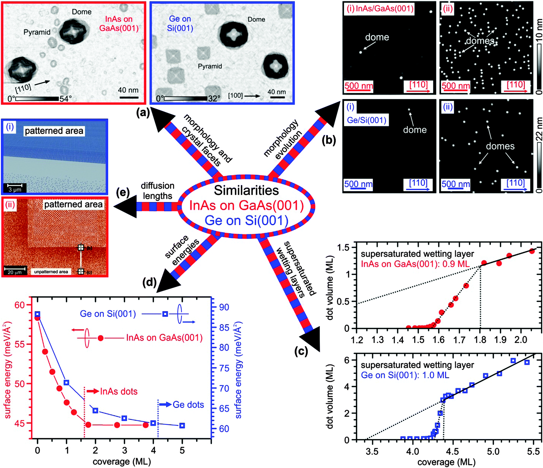 | ||
| Fig. 1 Similarities in the formation of NDs in the Ge on Si(001) system (blue) and the InAs on GaAs(001) system (red): (a) morphology and crystal facets, (b) ND morphology evolution, (c) supersaturation effects in the WL, (d) WL thickness-dependent surface energies, (e) surface diffusion lengths of the ad-atoms. Images and data taken from ref. 15, 17–20, 22. | ||
For both systems, various types of NDs were found that can be identified by the orientation of the crystal facets on the ND-surface. The two most prominent ND-types are so-called pyramids and domes. The former ones are, in general, smaller in volume and height-to-base-area aspect-ratio (AR). The surface of pyramids is formed by only one crystal facet family, {105} for SiGe pyramids on Si(001) substrates and {137} for InAs pyramids on GaAs(001) substrates. Fig. 1a depicts scanning tunneling microscopy (STM) images where the colour coding is correlated to the surface slope with respect to the substrate surface.17 In this way, pyramids can be distinguished by their light grey colour. The multi-faceted domes have larger volumes and ARs than pyramids (dark-grey NDs in Fig. 1a). For the SiGe system it was recently found that the larger domes are, with increasing deposited thickness of the epitaxial Ge film, the first energetically ND-species15 (we will elaborate this finding in more detail in Section 4.1).
In Fig. 1b atomic force microscopy (AFM) images depict the onset of dot nucleation in the InAs/GaAs and in the Ge/Si system. The first observed islands nucleating on the substrate surface are, in both systems, domes,15,17 which again points out the similarities of the growth systems.
Furthermore, in both systems, supersaturation effects in the initially formed WL are observed, i.e. the WL grows about 1 monolayer (ML) thicker than its equilibrium thickness. This can be traced, e.g. by photoluminescence (PL) spectroscopy (a detailed discussion of supersaturation effects will be given in Section 4), or, as shown in Fig. 1c, by ND volume analysis as a function of deposited film thickness as determined from AFM images.18,19 We explain in Section 4.1 that supersaturation effects in the WL are immediate consequences of the decreasing surface energies of the WL with increasing film thickness, a trend present in both material systems,20,21 see Fig. 1d.
Additionally, in both systems, the ND formation is, for typical growth temperatures, not limited by ad-atom surface diffusion lengths since those are on the order of several tens of micrometers.17,22 Such long diffusion lengths can be determined by the material flow into a nano-patterned area on the substrate that acts as a material sink. For both systems, the material diffusion leaves a zone depleted of material in the periphery of the nano-patterned area (see Fig. 1e).17,22
The heteroepitaxial Ge/Si and InAs/GaAs systems show striking similarities. In fact, such 2D WL plus 3D ND growth mode (to be explained in Section 3) occurs in a large variety of material systems, ranging from group-II–VI systems like e.g. CdSe on ZnSe,23 to nitride systems such as InN on GaN,24 metal systems like Au on Ni, or Au on Ag,25 to even ice on platinum.26
In the following we will focus on the Ge/Si model system, keeping in mind and stressing that growth phenomena described here might occur in a similar form in other strained epitaxial material systems.
3. Overview: relaxation mechanisms and ND formation in epitaxial thin films
There are two dominant deposition techniques to grow epitaxial semiconductor nanostructures: molecular beam epitaxy (MBE)27 and chemical vapor deposition (CVD).28 The latter uses gas sources such as GeH4 and SiH4 and thus the growth process involves molecule decomposition and hydrogen desorption. For more details, please refer to ref. 28. Here, we shall focus on the epitaxial growth processes occurring in MBE. In MBE, the constituent elements are deposited in the form of atomic or molecular beams onto a heated crystalline substrate to form thin epitaxial layers in ultra-high vacuum (UHV). The molecular beams typically stem from elemental sources that are either thermally evaporated via effusion cells or electron beam evaporators. Typical base pressures of growth chambers are a few 10−11 mbar. The key advantages of MBE are the capability to obtain very abrupt interfaces, to control precisely the composition, the layer thicknesses, doping, and to make use of the low growth rate for sub-atomic monolayer deposition. Typical growth rates of MBE lie between 0.02 and 2 Å s−1.Fig. 2 schematically depicts fundamental processes occurring during heteroepitaxial growth. Some basic processes such as absorption, desorption, diffusion and nucleation (see Fig. 2a–i) have already been detailed in previous reviews.10,11 To complete the picture, we additionally describe the role of surface reconstruction, plastic and elastic relaxation after a short introduction of growth modes occurring during heteroepitaxy.
 | ||
| Fig. 2 Scheme of the most important fundamental processes occurring during heteroepitaxial growth. (a) Absorption and (b) desorption of an ad-atom from a terrace site, (c) diffusion of an ad-atom, (d) ad-atom-clustering (ND nucleation), (e) attachment and (f) detachment of an atom from the ND, (g) deposition of an atom onto an ND, (h) attachment of an atom at a step-site and (i) at a kink site. (j–m) Relaxation mechanisms. Relaxation due to (j) surface reconstruction, (k) plastic relaxation, i.e. insertion of a dislocation, (l) elastic relaxation via 3D ND-formation and (m) intermixing with the substrate. | ||
The growth of epitaxial layers (epilayers) is classified into three different growth modes, named after their original investigators. These are the Frank–van der Merwe (FM), Volmer–Weber (VW), and Stranki–Krastanow (SK) growth modes, which can be described as 2D layer-by-layer growth, 3D ND growth, and 2D layer-by-layer plus 3D ND growth, respectively. The particular growth mode depends on the surface energies of the epilayer (or NDs) and the substrate, the interface energy between them, and the elastic strain energy induced in the epilayer and the substrate. In lattice matched systems, the growth mode is governed only by the surface and interface energies. If the sum of the epilayer surface energy γepi and the interface energy γint is lower than the energy of the substrate surface γsub, the epilayer wets the substrate and the FM growth mode occurs. A typical example for this mode is the growth of AlGaAs on GaAs(001). If γepi + γint > γsub, the epilayer avoids wetting the surface and the VW growth mode occurs. Typical examples for this growth mode are found for the growth of metals on insulators. In lattice mismatched systems, besides the surface and interface energies the growth mode also depends substantially on the elastic strain energy, which increases linearly with the layer thickness and quadratically with the strain induced by the lattice mismatch ε (ε = (aepi − asub)/asub, where aepi and asub are the lattice constant of the epilayer and substrate, respectively). Therefore, if the epilayer wets the substrate, it firstly grows layer-by-layer and after reaching a critical thickness coherent 3D islands form in order to release the strain energy, leading to the SK growth mode. As mentioned before, this growth mode is found in semiconductors and metal systems such as Ge/Si, InAs/GaAs, CdSe/ZnSe, GaN/AlN, Bi/GaP, Ag/Si, Au/Ni, Au/Ag and others. For instance, in the Ge/Si(001) system, Ge has a lattice constant 4.2% larger than that of Si and, hence, after the growth of about 4–5 monolayers of Ge, which is usually referred to as WL, 3D Ge islands with sizes of tens of nanometers form on top of the WL in order to relax the elastic energy. In addition, the elastic energy can also be released by plastic relaxation i.e. dislocation formation.
3.1 Plastic relaxation
We speak of plastic relaxation, when the mismatch strain is relieved by the formation of mismatch-dislocations. The initial cost of creating a mismatch-dislocation has to be counterbalanced by the energy gained by the strain relaxation caused by the dislocation. Thus, there exists a critical thickness tdisl of the deposited epifilm at which dislocation formation becomes energetically favorable in the strained epifilm. This thickness strongly depends on the strain in the epifilm and thus on the composition of the deposited SiGe alloy. The values for tdisl can go down to a few tenths of a nm for pure Ge films and hundreds of nm for highly diluted SiGe alloys grown on Si(001) substrates.29 When a Si1−xGex alloy is deposited onto a Si(001) substrate, it depends crucially on the Ge composition x of the alloy as well as on other parameters like the Ge growth temperature (TGe) or the Ge growth rate whether eventually plastic or elastic relaxation (tdisl or tWL) occurs. Plastic relaxation usually is the favorable relaxation mechanism when alloys with low Ge concentration (<15%) are deposited onto the Si substrate or when the surface kinetics is lowered due to low Si1−xGex alloy growth temperature or high deposition rate.Matthews and Blakesley29 described the dependence of tdisl on the Ge concentration of the epifilm. Their results are in good agreement with experimental values for rather high growth temperatures. For lower growth temperatures, where kinetic limitations play a role, the values of tdisl are significantly higher than the equilibrium values calculated in ref. 29.
The most common type of dislocation in the SiGe system are 60° line dislocations that glide in the respective {111} planes. Single dislocations tend to pile up into multiple dislocations, resulting in a network called cross-hatch pattern. Fig. 2k schematically depicts the formation of mismatch dislocations in the strained epifilm.
For the growth of nanostructures plastic relaxation is often undesired since mismatch-dislocations and threading arms might harm the electrical, optical and opto-electronic properties of the nanostructures.
3.2 Elastic relaxation
When elastic relaxation occurs after the deposited epifilm exceeds a critical WL thickness (tWL) the crystal remains coherent, i.e. free of dislocations. The accumulated strain is then relieved by the formation of 3D objects, called NDs or islands (Fig. 2l). For those NDs, the absence of lateral constraints allows the atomic planes to relax laterally, which reduces the elastic energy in the epifilm. The energetic benefit gained from the relief of the strain energy has to overcome the increase of surface energy due to the epifilm-surface-rearrangement.ND formation is often concomitant with significant intermixing with the substrate material – another path for strain relief in the nanostructures, see Fig. 2m. In this way the effective lattice mismatch and thus the strain are reduced. Nanotomography, a technique which reveals the 3D composition distribution30 within the island, showed that the NDs obtained at a high growth temperature of 740 °C have an average Ge concentration of less than 40%.31
For low mismatch strains (usually for Ge concentrations cGe <0.5) a growing film is unstable against surface perturbations. In this way NDs grow via the so-called Asaro–Tiller–Grinfeld (ATG) instability that does not exhibit any energetic barrier for ND growth (see e.g.ref. 11, 12 and 14).
The situation is different for higher strain values (cGe > 0.5). For larger mismatch values, a different process sets in, the nucleation of 3D NDs on a smooth WL. In contrast to the ATG process, ND nucleation in the SK growth mode has an activation energy that must be overcome.12,14
The epitaxially grown NDs can be identified by the respective crystal facets of which their surface consists. In the following we discuss low energy facets that are characteristic for SiGe NDs grown on Si(001) substrates.
In Fig. 3 scanning tunneling microscopy (STM) and atomic force microscopy (AFM) images of different fully developed NDs and NDs in transition shapes are presented in a sequence with increasing volume and AR.32
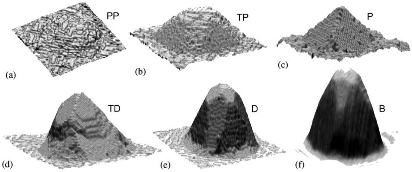 | ||
| Fig. 3 (a–f) Ge nanodots with increasing volume and aspect ratio. (a) Unfaceted pre-pyramids (PP), (b) not fully evolved transition pyramids (TP), (c) pyramid (P), (d) transition dome (TD), (e) dome (D) and (f) barn (B). Reprinted with permission from ref. 32. | ||
Prior to NDs with real crystalline facets, un-faceted nuclei, ad-atom accumulations usually called pre-pyramids are formed (see Fig. 3a and ref. 10–12). They transform during further material accumulation (e.g. due to material deposition or material diffusion) into clusters called transition pyramids, and further into pyramids (Fig. 3c) or hut clusters that are fully {105}-faceted.33 The discovery of the fully dislocation free NDs hut clusters by Mo et al.33 and domes (Fig. 3e) by Eaglesham et al.34 in 1990 was a starting point for extensive investigations of the heteroepitaxial growth of 3D nanostructures that last until today. The contact angle θ between the {105} facets and the (001) substrate surface is relatively shallow (11.3°). Thus, the AR of the pyramids is only 0.1. In contrast to pyramids, the base area of the hut clusters is rectangular, and not square. As a consequence, the AR of the hut clusters is smaller than the one for pyramids and always smaller than 0.1. Hut clusters are formed at relatively low temperatures (usually in a TGe window between 400 °C and 570 °C). In ref. 35 it is shown that the rectangular ND shape is caused by kinetic barriers at the ND edges. It was also found that an energetic barrier exists for the creation of larger facets.35,36 Thus, as more material is deposited, the system reacts either by nucleating new facets, i.e. by the increase of the ND density, or by elongation of the already existing structures. This implies that the growth on large facets is slower than on smaller ones, which implies that hut clusters strongly elongate.
As TGe increases the NDs become richer in their faceting behavior. This already implies that there exists an energetic barrier that must be overcome in order to create a new facet. At higher growth temperatures also the surface diffusion length increases and kinetic limitations can be more easily overcome. A multi-faceted dome34,37 that can be recognized in Fig. 3e has steeper facets with respect to the (001) surface. Those are {113} facets where θ is 25.3° and {15 3 23} facets (θ = 33.6°). Domes (AR ≈ 0.2, see Fig. 2(e)) that generally have larger volumes than pyramids transform from the latter via material accumulation at the apex of the pyramid (see Fig. 3d). This transition state is referred to as transition domes (TD, Fig. 3d).37,38 At growth temperatures higher than about 580 °C domes and pyramids (and transition domes) coexist, forming what is commonly called bimodal ND distribution.37 Domes are not the final evolution step with increasing ND volume. There seems to be several pathways that a dome can undergo once a critical volume is exceeded. On one hand a dislocation can be formed in the dome providing additional strain relief. Dislocated NDs are commonly termed “superdomes”.39 On the other hand, at higher growth temperatures, typically above 700 °C NDs with even steeper facets ({111} facets, 54.7° inclined to the substrate) than domes are found, which are referred to as “barns”.40 It was found that even barns are not the “final stable” ND shape, but in even more elevated temperatures so-called cupola NDs evolve. Their steepest {12 5 3} facets are up to 68° inclined with respect to the (001) surface.41
Until very recently the common interpretation was that NDs appear with increasing deposition amount in the order of pre-pyramids, pyramids, domes, barns and cupolas, since the increasing aspect ratio of the dots provides larger volumetric strain relaxation. However, this interpretation neglects the role of the wetting layer, as we describe in the following section.
4. WL build-up range and WL supersaturation
When Ge is grown onto the Si substrate, for the initial monolayers the total energy of the system (substrate plus epifilm) is lower than that of the same volume of relaxed bulk Ge and bulk Si even though Ge is fully strained within the first layers.20,42 Ge has a significantly smaller binding energy than Si and tends to float on the Si substrate, i.e. the system minimizes its energy when free Ge bonds are exposed on the surface and not free Si bonds. In this way the Ge layer shields the Si bonds and the effect of lowered energy is valid up to 5 MLs (see also Fig. 1d).20 This is also a reason why the Ge concentration in the WL is high, even for elevated growth temperatures.18 Beck et al.42 and Lu et al.20 have calculated the dependence of the chemical potential μWL of the WL (derivative of the elastic energy with respect to the volume) and the surface energy γWL of the WL as a function of the WL thickness, using ab initio density functional theory calculations. The chemical potential is especially low for the first two monolayers, lower than the one of unstrained Ge bulk. For a WL thickness N about 5 ML the value of μWL reaches the one of an infinitely thick pseudomorphic film. Due to the high energy of the Si bonds below the Ge WL the surface energy of the first few monolayers is higher than that for the thick film case where the value of γ for the WL is about 62 meV Å−2.20 The film-thickness dependent chemical potential and surface energy of the WL cause direct consequences on the initially ND growth.Fig. 4 depicts the evolution of the PL-emission of Si bulk, the WL and the NDs with increasing amount of deposited Ge. It is evident that the PL of the WL shifts with increasing WL thickness to lower energies due to decreased confinement energy.
 | ||
| Fig. 4 PL emission intensity evolution of Si bulk, the WL and the NDs as a function of the amount of deposited Ge. From the blue-shift of the WL-related PL signal it is evident that ∼1 ML of Ge is transferred from the WL to the NDs at their nucleation onset. | ||
Additionally, the WL PL emission energy abruptly shifts to higher energies concomitant with the appearance of the ND-PL (N ≈ 4.2 ML) that, as we show later, originates from dome shaped NDs. It was shown that this abrupt blue shift can be directly related to a material (Ge) transfer of 1 ML from the WL into the NDs,15 see also Fig. 1c. Thus, the WL actually becomes supersaturated in a coverage range between about 3.4 and 4.4 ML and it shrinks when dome NDs start to form. While we explain the origin of the supersaturated WL in the following section, we firstly stress why such a behavior in thin-film growth prior to the nanostructure formation is of such a high importance.
Supersaturation of Ge in the WL and the fact that the surface energy of the WL decreases with increasing film thickness N allows for the growth of very homogenous, but randomly distributed domes, as shown in the upper left corner of Fig. 5 and in Fig. 6. Moreover, due to the supersaturated WL it is also possible to create ordered NDs and ordered ND molecules on a pit-patterned substrate with an inter-dot spacing as high as several micrometers (right side of Fig. 5 and Fig. 8). Finally, the same accounts for the formation of in-plane Ge nanowires of a few micrometers (lower left of Fig. 5 and Fig. 9).
 | ||
| Fig. 5 Due to the supersaturated WL where the atoms in the top layers of the epifilm are only loosely bound, several novel types of nanostructure configurations can be fabricated: Very uniform domes for single dot applications, highly uniform and position-controlled dots with inter-pit-periods of several microns, nanowires of several micrometer length and ordered nanodot molecules. | ||
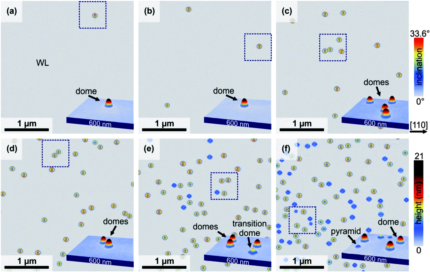 | ||
| Fig. 6 Unimodal ND shape and size distribution at the onset of ND nucleation. AFM micrographs in the surface-angle-image mode where the colour coding represents the local surface slope with respect to the (001) substrate surface. The colours were chosen in such a way that the different facets of the NDs can be distinguished easily. The inset shows three-dimensional images of the areas marked by the dotted squares. The amount of deposited Ge increases from (a) to (f) from 4.2 to 4.5 ML. | ||
 | ||
| Fig. 7 ND stability diagram. Critical ND volumes vs. WL thickness N. Gray regions indicate areas where no NDs can exist. For N < 3.8 ML metastable pyramids (mp) can only exist up to the maximum volume indicated by empty triangles. For N > 3.8 pyramids (p) are more stable than the WL above a certain minimum volume indicated by full triangles. Domes are stable for N > 2.7 and then only above the critical volume indicated by full circles. The critical volume for domes dramatically decreases with increasing N (see log scale). Thus, for a certain amount of deposited Ge, for example 3.5 ML as indicated by the dashed-arrowed line, for very small volumes only mp can exist, while domes can only exist for volumes larger than 104 nm3. For volumes in-between no NDs are energetically stable. Reprinted with permission from ref. 15. | ||
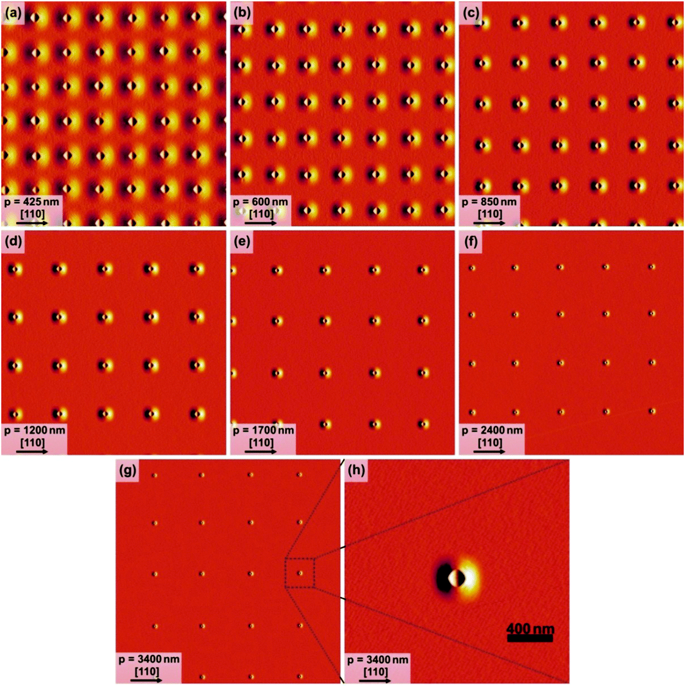 | ||
| Fig. 8 Strictly ordered NDs on a single sample with wide pit-period-variations. AFM images in derivative mode of a sample after Si buffer layer growth and the deposition of 3 ML of Ge at 700 °C. The pit-period increases from (a) 425 nm to (g) 3.4 μm. (h) presents a zoom-in of a pyramidal ND in a field with pit-period of 3.4 μm. No defects in the growth such as secondary NDs between the pits are observed. Reprinted with permission from ref. 43. | ||
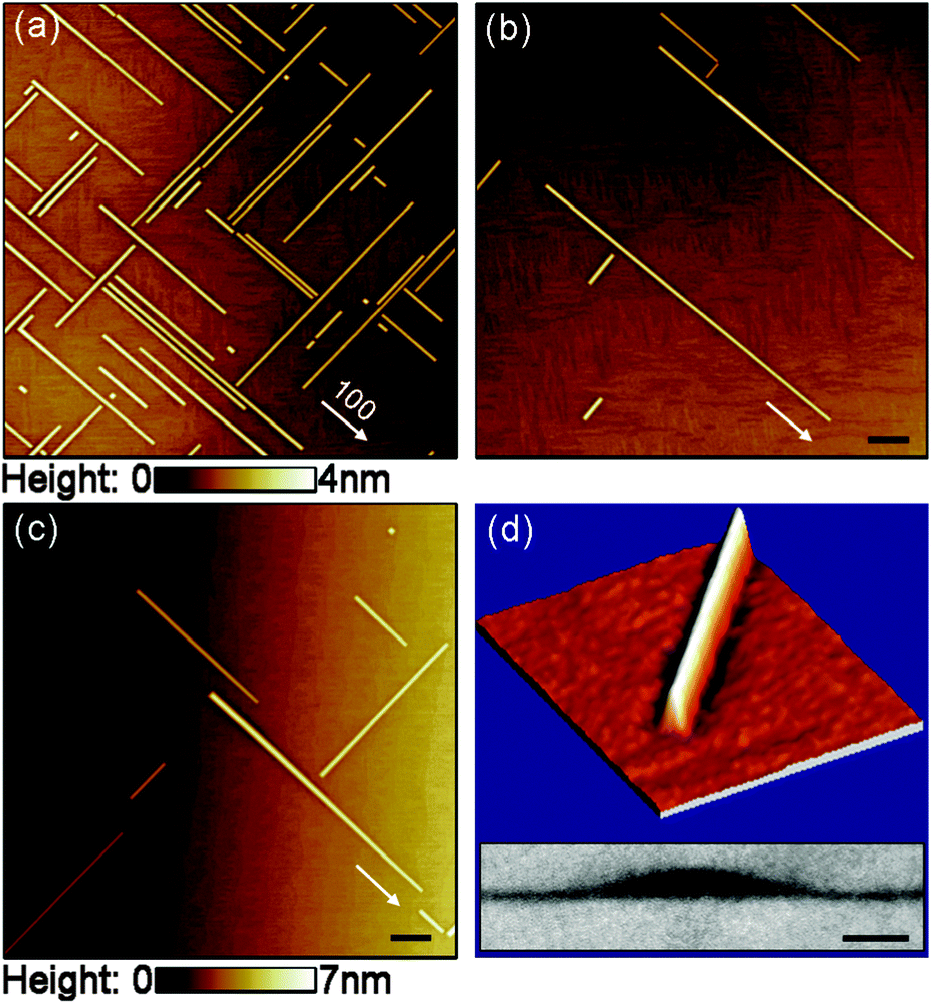 | ||
| Fig. 9 AFM images of Ge wires forming on Si(001) substrates after 12 h annealing. Atomic terraces are parallel to the (001) plane and atomic steps on the WL are well visible. (a) High and (b) low density of Ge wires on Si(001) with a nominal miscut angle of less than 0.05°. (c) Tapered Ge wires on Si(001) with a nominal miscut angle of less than 0.5°. The wires grow laterally along either of the two 〈100〉 directions as indicated by the arrows and their surface is composed of four {105} facets. Scale bar: 200 nm. (d) 3D AFM image of an individual Ge wire. The inset shows a cross-sectional TEM image of the Ge wire capped with Si at 300 °C, showing a sharp Si/Ge interface and an inclination angle of 11.3° between {105} facets and the substrate plane. Scale bar: 5 nm. Reprinted with permission from ref. 16. | ||
4.1 WL supersaturation and highly homogeneous nanodot sizes
Whether an ND is stable or not depends on the relationship between the volumetric elastic energy of the ND and the flat film, as well as on the increase of surface energy due to the ND's geometry. The relation can be written as| Δ = V·(ρND − ρWL) + S·γND – B·γWL |
For a WL thickness N of more than 4 ML there always exists a finite volume for which ND nucleation is favored. In this case, the theoretically predicted sequence of evolving NDs is equal to the one shown in Fig. 3, i.e. pre-pyramids (Fig. 3a) nucleate on the substrate, and evolve via transition pyramids with unfinished facets (Fig. 3b) into pyramids (Fig. 3c) which thereafter transform (Fig. 3d) further into multifaceted domes (Fig. 3e). However, we stressed above that the surface energy density of the WL strongly depends on the actual thickness of the WL. Thus, if one takes into account the thickness-dependence of the elastic energy density and the surface energy density of the WL, it is possible to determine the ND stability also for a smaller WL thickness which is relevant to determine the real nucleation and kinetic evolution of the epitaxial semiconductor NDs. For increasing N, γWL decreases and ρWL increases.20,42 Thus, it is for just small enough N not guaranteed that the volumetric term in the equation above favors ND formation – even at large ND volumes.15 Additionally, the different surface energy densities and elastic energy densities for the different ND types (pyramids and domes, i.e. different aspect ratio and facets) have to be taken into account for determining the stability of a ND.
Fig. 6 presents AFM images of NDs occurring at the onset of ND nucleation, i.e. between 4.2 ML and 4.5 ML of Ge deposited at TGe = 700 °C. The colour coding for the surface angle image mode (SAI), where the local surface slope with respect to the substrate surface is calculated for every point in the scan, was chosen in a way that each colour corresponds to one of the well-known crystalline facets of the NDs (blue: {105}, yellow: {113} and red {15 3 23}). From the micrographs it is evident that the initially nucleated NDs are actually domes (Fig. 6a–d), while at higher coverage (Fig. 6e and f) pyramids with more shallow facets also appear (blue colour). The insets in Fig. 6 are 3D-AFM images. From the insets that present the area that is marked in the SAI images by the dotted squares as 3D height images, we clearly see that the first appearing domes are higher than the pyramids.
Fig. 7 presents a ND stability diagram in which the critical volume is plotted at which a ND of a certain type is more stable than the flat epifilm for a given N (note the logarithmic ordinate). Grey-shaded areas mark regions where WL thickening is always favored and no NDs are stable regardless of their volume. For low N small {105}-faceted clusters are more stable than the WL, but only if their volume is below a certain critical volume. The reason for this behavior is the very low surface energy of the reconstructed and compressed {105}-surface that favors pyramid formation, as long as their volume is smaller than the one indicated in Fig. 7 by the empty triangles.15 Since the critical upper volume-boundary for such NDs is small and can be reached for example by material fluctuations during the growth these pyramids are considered to be metastable pyramids (mp). Red full dots (full green triangles) in Fig. 7 mark the volumes above which domes (pyramids) are more stable than the flat epifilm. Pyramids are unstable for N < 3.8 ML and domes are stable for N > 2.7 ML. However, the critical volume for dome formation is very large for small WL thickness due to the strongly bound atoms in the WL and it decreases rapidly with increasing thickness. One can predict from Fig. 7 that at N = 2.7 ML the WL will further thicken and dome nucleation will happen on a supersaturated WL. Additionally, after the dome formation, WL thinning has to be expected. Following the dashed-arrowed line in Fig. 7, metastable pyramids are formed already at very small volumes. Between 2.7 ML and 3.8 ML there exists a volumetric gap for which no NDs are stable. With increasing N this gap reduces and at N ∼ 3.8 ML pyramids can enlarge their volume and reach the critical volume for dome formation. If N is slightly smaller than 3.8 ML then the small volumetric gap can be closed by material fluctuations. In both cases, WL thinning and dome formation prior to pyramid formation is predicted, as observed by AFM and PL experiments (Fig. 4 and 6). For lower TGe (625 °C) metastable pyramids are observed already for N = 2 ML.15 Since there are less thermal fluctuations at low TGe the lifetime of the metastable pyramids is increased. It was found that for lower TGe domes only form at a WL thickness of about 4.8 ML.15 This is due to the fact that at lower TGe the surface kinetics are slow and hence, more time is needed to collect material that is necessary to form the domes. Consequently, the WL supersaturates even more. It was shown15 that when the growth rate is reduced by a factor of 5 then the WL becomes less supersaturated which can be explained by the increased effective time in which Ge can diffuse to the ND which makes the formation of domes easier. To determine the metastability of the pre-pyramids, the small mp's formed at 2.1 ML and 3.5 ML were in situ annealed.15 While the mp's formed at 2.1 ML form back to a 2D-WL, the ones formed at 3.5 ML transform into domes, as predicted in the ND stability diagram in Fig. 7.15
In the following we stress the importance of understanding WL supersaturation effects and ND stability for the formation of dots and dot-molecules with large inter-structure periods and also for the formation of novel single crystalline in-plane Ge NWs.
4.2 Ordered nanodots and nanodot molecules with large inter-dot spacing
Position control and ordering of NDs and also ND-molecules on Si substrates is an important precondition to integrate them into modern Si technology, because of the mandatory addressability.7,43 An additional advantage of ordered dots is the significantly improved size and chemical composition uniformity.17,22,31,43 In order to address a single ND or ND-molecule it is beneficial to be able to tune the inter-dot-distance over a wide range. Ordered NDs, especially group III–V NDs with direct band gaps, grown on pit-patterned substrates with pit-periods larger than 1 μm can be used for devices with novel functionalities, such as single photon emitters.3One of the most promising methods to accurately position NDs is the growth of Ge on pit-patterned Si substrates (see Fig. 5, upper right panel) where perfectly ordered NDs can be obtained, if a number of pre-conditions concerning the pit-pattern are fulfilled.43 For instance, the pit-opening diameter after the growth of a Si buffer layer needs to be about twice the ND diameter and the respective pit-sidewalls should not be too steep, i.e. between 5° and 18°.43 On the other hand, to obtain ND-molecules nucleating around pits (Fig. 5, lower right) it is necessary that the pit-sidewalls are steeper than about 30° with respect to the (001) surface.44 This condition favors the nucleation at the pit-rim for two reasons. The strain induced by the dot in the substrate can be relaxed effectively by the pits and the initial relaxation of the WL favor ND nucleation at the rim of the pits.44,45 Furthermore, the amount of deposited Ge, the growth rate and also the TGe have to be adjusted for successful growth of ordered nanostructures.43
As discussed in Section 4.1, ND formation on planar substrates is preceded by the formation of a supersaturated WL. On pit-patterned substrates, dots in pits and dot-molecules bound to the rim of pits can only grow to a certain volume before they eventually start to form dislocations.11,12,14,39 Thus, if the deposited material exceeds the volume that is needed to achieve a critical WL thickness (∼4.2 ML) plus the material that is needed to form the NDs in the pits, secondary ND nucleation will take place between the pits.43
Therefore, two conclusions for the growth of NDs and dot-molecules on patterned fields with large pit-periods can be drawn: firstly, the growth rate must not be too high in order to allow an effective Ge transfer to the material sinks (pits) before the ad-atoms become covered by the next deposited layer;22,43 secondly, even for very low growth rates, at very large pit-periods of several micrometers, ND formation on the flat regions is unavoidable if the amount of deposited Ge is so high that the WL between the pits reaches the critical thickness for ND formation.22,43 In fact, N has to be smaller than 4.2 ML, but larger than 3 ML, because below this thickness atoms are more effectively bound in the WL (see discussion above), which partially prevents Ge diffusing to the pits. For 3 < N < 4.2 ML the Ge ad-atoms in the topmost layers are, due to their lower surface energy, only weakly bound and will contribute to ND growth in the pits. Fig. 8 presents perfectly ordered pyramids for pit-periods varying from 425 nm (Fig. 8a) to 3400 nm (Fig. 8g and h). This highlights the great advantage of using supersaturation effects in the WL for ordered ND growth: The inter-nanostructure distance can be varied a few hundred nanometers to several micrometers, while obtaining perfectly uniform NDs. Note that the fields shown in Fig. 8 were located on the same sample and, thus, were grown in the same MBE growth run under the aforementioned growth conditions, i.e. 3 ML of Ge were grown at TGe = 700 °C.43
4.3 Nanowires
As discussed above, the supersaturated WL leads to the formation of homogenous dome-shaped NDs and the careful control of the WL supersaturation can avoid the unwanted ND formation on flat regions between pits. All these experiments were performed at relatively high TGe, where the main driving force for ND growth is elastic strain relaxation. At lower TGe (<570 °C), on supersaturated WLs {105}-faceted hut clusters are observed and the elastic energy release in such shallow structures is limited.10 By using real-time scanning tunneling microscopy, McKay et al. observed that hut clusters grow slowly at a decreasing rate during annealing experiments, depleting gradually the Ge WL supersaturation.46 Although the growth rate was only a few nm in tens of hours of annealing at 450 °C, it demonstrated that the material could transfer from the WL into the 3D NDs and cause their elongation.46 Thus, the next logic question was whether one can keep the hut clusters elongating and obtain Ge “hut wires” or NWs by annealing.16 In the following, we show that, under certain conditions, it is indeed possible to obtain micrometer long Ge NWs by means of annealing the Ge WL.16A 4.4 ML thick, supersaturated Ge WL was initially deposited with a growth rate of 0.06 Å s−1 at TGe = 570 °C. The deposited Ge amount is slightly smaller than the critical thickness of 4.5 ML for the formation of 3D Ge hut clusters at TGe = 570 °C. After Ge deposition the substrate temperature is slightly lowered and kept at 560 °C for 12 hours. During the in situ annealing, the supersaturated Ge in the 2D WL transforms into 3D NDs with surfaces consisting of four {105} facets, as confirmed by cross-sectional TEM (Fig. 9d). Such NDs grow randomly along either of the two in-plane 〈100〉 directions (Fig. 9a). The length of the NWs is typically already a few hundreds of nanometers after 1 h annealing and reaches the micrometer range in 3 hours. Further annealing leads to only a limited increase in NW length. This is attributed to the fact that, as Ge moves into the NWs, the WL is consumed leading to a gradual reduction of the growth rate due to the depletion of the Ge supersaturation.46 All the NWs are homogenous in height (width) and the statistical analysis shows an average height h of 1.86 nm (and a derived base width b = 18.6 nm) with a low standard deviation (0.14 nm). Furthermore, the NW density can be tuned by the initially deposited amount of Ge. A decreased amount of supersaturated Ge results in a reduced island nucleation rate.47 Under these conditions the NW density drops, but the maximum wire length increases up to ∼2 μm, showing an aspect ratio of NW length L to height h of ∼1000 (Fig. 9b). By increasing the initial Ge amount, a larger density of comparatively shorter wires is obtained, which is attributed to the increased probability of “collisions” between growing NWs and the reduced amount of supersaturated material available for each NW.16
The individual NWs have a constant height (width) as long as they grow on the same atomic terrace. When they cross a lower (higher) atomic step (0.14 nm high), the NW height is observed to increase (decrease) by an atomic layer thickness. On substrates with larger terraces, all the NWs are expected to have a constant height. On substrates with smaller terraces, tapered NWs are instead observed (Fig. 9c). Finally, we point out that the Ge NWs do not consist of pure Ge since Si–Ge intermixing takes place during Ge deposition and the subsequent annealing process. Selective wet chemical etching in a H2O2 solution shows that the Ge content is higher than 65% even at the base which is known to have the lowest Ge content.30,31
The observation of Ge NWs with a homogenous base width (height) can be interpreted in a thermodynamic model, by comparing the energy difference ΔE (elastic energy, surface energy and edge energy) between a NW on an N-layer thick WL, and a configuration where the same material is instead spread on the WL, creating a region with N + 1 layers.16 From the calculations, we see that ΔE is negative for NW base widths larger than 8 nm, indicating that NW formation is energetically favourable vs. WL thickening. There exists a theoretical base width of bmin = 16.3 nm, minimizing the energy of the NW at a fixed volume (Fig. 10). Remarkably, the theoretical value for bmin, 16.3 nm, is very close to the experimentally observed value of 18.6 nm. For N = 4, the surface energy difference (per unit area) between Ge (105) and (001) is negative (−4.5 meV Å−2). This implies that the driving force for NW formation is the reduction of surface energy, rather than strain relaxation.16
 | ||
| Fig. 10 Energy difference ΔE (divided by volume) between a NW and a 2D configuration of equal V is plotted vs. base width b. The inset illustrates the structures used in the model: truncated wires with only two {105} facets. Points along the curve in the plot represent wires of different length but same volume, as sketched in the inset. The black filled circle indicates the base width bmin, corresponding to the minimum-energy configuration. bmin is volume independent. Reprinted with permission from ref. 16. | ||
Considering their ultra-small and uniform cross section together with advantages of catalyst free and horizontal growth on Si(001), such Ge NWs are expected to be excellent candidates for the investigation of interesting physical properties and the realization of novel electronic devices. For instance, Kloeffel et al.48 suggested that such systems could support helical modes, making them appealing for the observation of exotic quantum states, like Majorana fermions.48 Furthermore, the positioned growth of Ge NWs can be expected, similar to the growth of site-controlled Ge NDs as discussed in Section 4.2. Such position control would allow their large scale integration.
4.4 Bundles
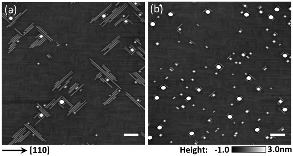
In the previous section we have seen that the annealing temperature (TA) is crucial in obtaining the Ge NWs. By lowering the TA, Ge bundles are obtained. Fig. 11a–d shows the AFM images of Ge nanostructures observed after 12 h annealing of the supersaturated 4.4 ML thick Ge WL at 500, 520, 540 and 550 °C, respectively. The Ge WL growth temperature is 560 °C for all these samples. For a lower TA of 500 and 520 °C, “bundles” consisting of tens of closely packed Ge NWs are observed. They are randomly distributed on the surface along either of the two 〈100〉 directions and well separated by planar WL regions. There are about 0.1 and 0.2 ML of Ge transferred from the WL into the bundles, respectively. With increasing TA, the number of wires in a bundle decreases and, at 550 °C, wires are almost isolated, similar to the aforementioned observations for TA = 560 °C (Section 4.3). In addition, the Ge transferred from the WL into bundles (or NWs) and the bundle density increases with increasing TA. The former is due to the increased surface diffusion length and the latter is attributed to the increased nucleation rate at increased temperature.47 | ||
| Fig. 11 AFM images showing horizontal Ge nanowire bundles or isolated Ge nanowires on Si(001) substrates obtained after 12 h annealing of a Ge wetting layer at different temperatures: 500 (a), 520 (b), 540 (c), and 550 °C (d), and after 1 h (e), 12 h (b) and 66 h (f) annealing at 520 °C. The Ge wetting layer was obtained by depositing 4.4 ML Ge at a substrate temperature of 560 °C. Scale bar: 250 nm. Reprinted with permission from ref. 50. | ||
Furthermore, we investigate the evolution of NW bundles with annealing time. Fig. 11e, b and f show AFM images of Ge nanostructures grown at 560 °C after 1 h, 12 h and 66 h annealing at 520 °C, respectively. A 1 h annealing step leads to single Ge hut clusters and bundles containing only a few hut clusters. After 12 h annealing, the number of NWs in each bundle is significantly increased, indicating that new NWs nucleate adjacent to the preexisting ones. Simultaneously, the NWs grow in length. With further annealing (66 h), the NWs keep elongating and reach lengths up to a few micrometers. However, no distinct increase of the number of NWs per bundle is observed (Fig. 11b and f).
This novel phenomenon of NW-bundling is again linked to supersaturation effects of the Ge WL and can be explained by a thermodynamic wave model.49 In the wave model, starting from an isolated wire, lateral wave-like replication takes place gradually generating closely-packed satellites with equal base widths (Fig. 12a). In Fig. 12b the energy difference (elastic energy, surface energy and edge energy) between an isolated NW and a NW with two satellites is plotted as a function of the satellite size at different WL thickness (expressed in number N of ML's). Below a critical WL thickness of about N = Nc≈4.2 ML, the wave-propagation or bundle formation raises the energy of the system, and above it, however, the wave propagates generating satellites with a preferred base size of about 10 nm at N = 4.4 ML. When the residual WL thickness is larger than Nc, i.e. the transferred Ge material from the WL into the bundles is less than 0.2 ML, as shown in Fig. 11a, b and e the wave keeps propagating. After 12 h annealing at TA = 520 °C the residual Ge WL approaches Nc = 4.2 ML. Therefore, further annealing does not promote additional wave propagation and only NW elongation is still energetically favorable (see Section 4.3). This is nicely confirmed by the experimental data of Fig. 11b and f, where the number of NWs in each bundle is unchanged, while their lengths keep increasing. In addition, the predicted base value of about 10 nm is also in perfect agreement with the experimental observations (Fig. 11a, b, and f).
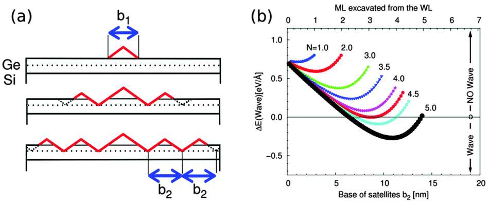 | ||
| Fig. 12 (a) 2D sketch of the creation of a wave starting from a single precursor of base b1 lying on an N-ML-thick wetting layer. (b) Difference in total energy between an isolated wire and a wire with two satellites of variable base. In (b) the red curve tangent to the zero value is the one obtained for N = Nc = 4.25 ML. Reprinted with permission from ref. 50. | ||
For high TA, i.e. between 550 °C and 560 °C, the bundle-wave does not form at early annealing stages even when the WL thickness is still greater than 4.2 ML. We speculate that at high enough TA, as soon as the wave process is attempted, e.g. by expelling WL ad-atoms close to the long sides of the NW, highly mobile ad-atoms quickly diffuse away, without leading to actual nucleation of a new satellite NW. As the process proceeds, the WL becomes thinner and lateral replication eventually becomes energetically unfavorable.
In this section we have demonstrated that variation of TA leads to the observation of novel bundle-structures. Thus, the remaining parameter influencing NW and NW-bundle growth from supersaturated WLs remains the initial Ge deposition temperature TGe. At a lower TGe of 540 °C and after a 12 h annealing step at 520 °C, the same structures were observed as shown in Fig. 11b. At a higher TGe (600 °C), we observed Ge bundles surrounding pyramids or domes (Fig. 13a), indicating that pyramids or domes can be considered as “seeds” for the bundle-formation. The Ge bundles themselves are similar to the ones shown in Fig. 11b except that less NWs contribute to the bundles, caused by a diminished material transfer from the supersaturated WL. This is due to a reduced WL thickness, i.e., a reduced supersaturation of the Ge WL at elevated growth temperature of 600 °C. The critical thickness for ND formation is decreased to 4.3 ML and sparse pyramids and domes are already formed for N = 4.4 ML. If we slightly increase the N to 4.5 ML and then anneal for 12 h at 520 °C, we observe only short NWs around the pyramids or domes (Fig. 13b). Very little material can be transferred from the WL to the wires, since the domes and pyramids consume almost all supersaturated Ge (see Sections 4, 4.1 and ref. 15).
 | ||
| Fig. 13 AFM images showing the combinations of Ge NDs and bundles (a) or NWs (b) on Si(001) obtained after 12 h annealing at 520 °C. The initial Ge deposition temperature is 600 °C and the deposited Ge amounts are 4.4 (a) and 4.5 (b) ML, respectively. The NDs are already formed after the Ge deposition at 600 °C. | ||
5. Summary and outlook
In this article, we have reviewed the recent progress in epitaxial growth of semiconductor nanostructures, focusing on the Ge/Si model system. In particular, we have shown that the metastable or supersaturated Ge WL plays a key role in determining the nucleation and growth of NDs and NWs. At higher growth temperatures, mainly driven by the elastic energy relaxation, the metastable material from the WL abruptly evolves into 3D NDs with steeper facets, leading to the formation of homogeneous NDs on planar substrates. A careful control of the metastable material allows us to obtain perfectly site-controlled NDs or ND molecules on pit-patterned substrates over a broad range of pit periods. At lower growth temperatures, the elastic energy relaxation is negligible because of the shallow shape of the {105} facetted huts or NWs. Instead, the low surface energy of the compressively strained Ge {105} facets drives the transfer of supersaturated material from the WL into the 3D structures, successfully explaining the observation of Ge NWs and bundles. By a close comparison between the Ge/Si and InAs/GaAs growth system and as a consequence of the striking similarities between them we imply that the novel phenomena observed in Ge/Si(001) and described in this review could also appear in other heteroepitaxial semiconductor systems.Acknowledgements
Jianjun Zhang acknowledges vice-chancellor's fellowship from University of New South Wales and Moritz Brehm acknowledges financial support from the Austrian Science Fund (FWF): J3328-N19. The authors thank A. Rastelli for fruitful discussions.References
- D. Bimberg, J. Phys. D: Appl. Phys., 2005, 38, 2055 CrossRef CAS.
- H. Y. Liu, S. L. Lew, T. Badcock, D. J. Mowbray, M. S. Skolnick, S. K. Ray, T. L. Choi, K. M. Groom, B. Stevens, F. Hasbullah, C. Y. Jin, M. Hopkinson and R. A. Hogg, Appl. Phys. Lett., 2006, 89, 073113 CrossRef PubMed.
- P. Michler, A. Kiraz, C. Becher, W. V. Schoenfeld, P. M. Petroff, L. D. Zhang, E. Hu and A. Imanoglu, Science, 2000, 290, 2282–2285 CrossRef CAS PubMed.
- A. J. Bennetta, D. C. Unitta, P. Atkinson, D. A. Ritchie and A. J. Shields, Opt. Express, 2005, 13, 50 CrossRef.
- R. M. Stevenson, R. J. Young, P. Atkinson, K. Cooper, D. A. Ritchie and A. J. Shields, Nature, 2006, 439, 179 CrossRef CAS PubMed.
- O. G. Schmidt and K. Eberl, IEEE Trans. Electron Devices, 2001, 48, 1174 CrossRef.
- V. Jovanović, C. Biasotto, L. K. Nanver, J. Moers, D. Grützmacher, J. Gerharz, G. Mussler, J. van der Cingel, J. J. Zhang, G. Bauer, O. G. Schmidt and L. Miglio, IEEE Electron Device Lett., 2010, 31, 1083 CrossRef.
- G. Pernot, M. Stoffel, I. Savic, F. Pezzoli, P. Chen, G. Savelli, A. Jacquot, J. Schumann, U. Denker, I. Mönch, Ch. Deneke, O. G. Schmidt, J. M. Rampnoux, S. Wang, M. Plissonnier, A. Rastelli, S. Dilhaire and N. Mingo, Nat. Mater., 2010, 9, 491 CrossRef CAS PubMed.
- G. Katsaros, P. Spathis, M. Stoffel, F. Fournel, M. Mongillo, V. Bouchiat, F. Lefloch, A. Rastelli, O. G. Schmidt and S. De Franceschi, Nat. Nanotechnol., 2010, 5, 458 CrossRef CAS PubMed.
- B. Voigtländer, Surf. Sci. Rep., 2001, 43, 127 CrossRef.
- C. Teichert, Phys. Rep., 2002, 365, 335 CrossRef CAS.
- J. Stangl, V. Holy and G. Bauer, Rev. Mod. Phys., 2004, 76, 725–783 CrossRef CAS.
- V. Shchukin, E. Schöll and P. Kratzer, in Semiconductor Nanostructures, ed. D. Bimberg, Springer, Berlin, 2008, pp. 1–39 Search PubMed.
- J.-N. Aqua, I. Berbezier, L. Favre, T. Frisch and A. Ronda, Phys. Rep., 2013, 522, 559 CrossRef PubMed.
- M. Brehm, F. Montalenti, M. Grydlik, G. Vastola, H. Lichtenberger, N. Hrauda, M. J. Beck, T. Fromherz, F. Schäffler, L. Miglio and G. Bauer, Phys. Rev. B: Condens. Matter Mater. Phys., 2009, 80, 205321 CrossRef.
- J. J. Zhang, G. Katsaros, F. Montalenti, D. Scopece, R. O. Rezaev, C. Mickel, B. Rellinghaus, L. Miglio, S. De Franceschi, A. Rastelli and O. G. Schmidt, Phys. Rev. Lett., 2012, 109, 085502 CrossRef CAS.
- S. Kiravittaya, A. Rastelli and O. G. Schmidt, Rep. Prog. Phys., 2009, 72, 046502 CrossRef.
- M. Brehm, M. Grydlik, H. Groiss, F. Hackl, F. Schäffler, T. Fromherz and G. Bauer, J. Appl. Phys., 2011, 109, 123505 CrossRef PubMed.
- E. Placidi, F. Arciprete, V. Sessi, M. Fanfoni, F. Patella and A. Balzarotti, Appl. Phys. Lett., 2005, 86, 241913 CrossRef PubMed.
- G. H. Lu, M. Cuma and F. Liu, Phys. Rev. B: Condens. Matter Mater. Phys., 2005, 72, 125415 CrossRef.
- L. G. Wang, P. Kratzer, M. Scheffler and N. Moll, Phys. Rev. Lett., 1999, 82, 4042 CrossRef CAS.
- M. Grydlik, M. Brehm, F. Hackl, F. Schäffler, G. Bauer and T. Fromherz, Phys. Rev. B: Condens. Matter Mater. Phys., 2013, 88, 115311 CrossRef.
- M. Strassburg, T. Deniozou, A. Hoffmann, R. Heitz, U. W. Pohl, D. Bimberg, D. Litvinov, A. Rosenauer, D. Gerthsen, S. Schwedhelm, K. Lischka and D. Schikora, Appl. Phys. Lett., 2000, 76, 685 CrossRef CAS PubMed.
- E. Dimakis, E. Iliopoulos, K. Tsagaraki, T. Kehagias, P. Komninou and A. Georgakilas, J. Appl. Phys., 2005, 97, 113520 CrossRef PubMed.
- S. G. Corcoran, G. S. Chakarova and K. Sieradzki, Phys. Rev. Lett., 1993, 71, 1585 CrossRef CAS.
- S. Haq, J. Harnett and A. Hodgson, Surf. Sci., 2002, 505, 171 CrossRef CAS.
- P. Frigeri, L. Seravalli, G. Trevisi and S. Franchi, in Comprehensive Semiconductor Science and Technology, ed. P. Bhattacharya, R. Fornari and H. Kamimura, Elsevier, Amsterdam, 2011, pp. 480–522 Search PubMed.
- D. M. Dobkin and M. K. Zuraw, Principles of Chemical Vapor Deposition, Springer, 2003 Search PubMed.
- J. W. Matthews and A. E. Blakesley, J. Cryst. Growth, 1974, 27, 118 CAS.
- A. Rastelli, M. Stoffel, A. Malachias, T. Merdzhanova, G. Katsaros, K. Kern, T. H. Metzger and O. G. Schmidt, Nano Lett., 2008, 8, 1404 CrossRef CAS PubMed.
- J. J. Zhang, F. Montalenti, A. Rastelli, N. Hrauda, D. Scopece, H. Groiss, J. Stangl, F. Pezzoli, F. Schäffler, O. G. Schmidt, L. Miglio and G. Bauer, Phys. Rev. Lett., 2010, 105, 166102 CrossRef CAS.
- A. Rastelli, M. Stoffel, G. Katsaros, J. Tersoff, U. Denker, T. Merdzhanova, G. S. Kar, G. Costantini, K. Kern, H. von Känel and O. G. Schmidt, Microelectron. J., 2006, 37, 1471–1476 CrossRef CAS PubMed.
- Y. W. Mo, D. E. Savage, B. S. Swartzentruber and M. G. Lagally, Phys. Rev. Lett., 1990, 65, 1020 CrossRef CAS.
- D. J. Eaglesham and M. Cerullo, Phys. Rev. Lett., 1990, 64, 1943 CrossRef CAS.
- M. Kästner and B. Voigtländer, Phys. Rev. Lett., 1999, 82, 2745 CrossRef.
- D. E. Jesson, G. Chen, K. M. Chen and S. J. Pennycook, Phys. Rev. Lett., 1998, 80, 5156 CrossRef CAS.
- G. Medeiros-Ribeiro, A. M. Bratkovski, T. I. Kamins, D. A. A. Ohlberg and R. S. Williams, Science, 1998, 279, 353 CrossRef CAS.
- F. M. Ross, R. M. Tromp and M. C. Reuter, Science, 1999, 286, 1931 CrossRef CAS.
- T. I. Kamins, G. Medeiros-Ribeiro, D. A. A. Ohlberg and R. S. Williams, J. Appl. Phys., 1999, 85, 1159 CrossRef CAS PubMed.
- E. Sutter, P. Sutter and J. E. Bernard, Appl. Phys. Lett., 2004, 84, 2262 CrossRef CAS PubMed.
- M. Brehm, H. Lichtenberger, T. Fromherz and G. Springholz, Nanoscale Res. Lett., 2011, 6, 70 CrossRef PubMed.
- M. J. Beck, A. van de Walle and M. Asta, Phys. Rev. B: Condens. Matter Mater. Phys., 2004, 70, 205337 CrossRef.
- M. Grydlik, G. Langer, T. Fromherz, F. Schäffler and M. Brehm, Nanotechnology, 2013, 24, 105601 CrossRef PubMed.
- G. Vastola, M. Grydlik, M. Brehm, T. Fromherz, G. Bauer, F. Boioli, L. Miglio and F. Montalenti, Phys. Rev. B: Condens. Matter Mater. Phys., 2011, 84, 155415 CrossRef.
- B. Yang, F. Liu and M. G. Lagally, Phys. Rev. Lett., 2004, 92, 025502 CrossRef.
- M. R. McKay, J. A. Venables and J. Drucker, Phys. Rev. Lett., 2008, 101, 216104 CrossRef.
- J. Tersoff and F. K. LeGoues, Phys. Rev. Lett., 1994, 72, 3570 CrossRef CAS.
- C. Kloeffel, M. Trif and D. Loss, Phys. Rev. B: Condens. Matter Mater. Phys., 2011, 84, 195314 CrossRef.
- G. Chen, B. Sanduijav, D. Matei, G. Springholz, D. Scopece, M. J. Beck, F. Montalenti and L. Miglio, Phys. Rev. Lett., 2012, 108, 055503 CrossRef CAS.
- J. J. Zhang, A. Rastelli, O. G. Schmidt, D. Scopece, L. Miglio and F. Montalenti, Appl. Phys. Lett., 2013, 103, 083109 CrossRef PubMed.
| This journal is © The Royal Society of Chemistry 2015 |