 Open Access Article
 This Open Access Article is licensed under a
 Creative Commons Attribution 3.0 Unported Licence
Surface defects and their impact on the electronic structure of Mo-doped CaO films: an STM and DFT study
Yi
Cui
a,
Xiang
Shao
a,
Stefano
Prada
b,
Livia
Giordano
b,
Gianfranco
Pacchioni
b,
Hans-Joachim
Freund
a and
Niklas
Nilius
*ac
aFritz-Haber-Institut der Max-Planck-Gesellschaft, Faradayweg 4-6, D-14195 Berlin, Germany
bDipartimento di Scienza dei Materiali, Università di Milano-Bicocca, via Cozzi 53, 20125 Milano, Italy
cInstitut für Physik, Carl von Ossietzky Universität Oldenburg, D-26111 Oldenburg, Germany. E-mail: niklas.nilius@uni-oldenburg.de
First published on 6th May 2014
Abstract
The functionality of doped oxides sensitively depends on the spatial distribution of the impurity ions and their interplay with compensating defects in the lattice. In our combined scanning tunneling microscopy (STM) and density functional theory (DFT) study, we analyze defects occurring in Mo-doped CaO(001) films at the atomic scale. By means of topographic imaging, we identify common point and line defect in the doped oxide, in particular Mo donors and compensating Ca vacancies. The influence of charged defects on the oxide electronic structure is analyzed by STM conductance spectroscopy. The experimentally observed defect features are connected to typical point defects in the CaO lattice by means of DFT calculations. Apart from the identification of individual defects, our study reveals a pronounced inhomogeneity of the oxide electronic structure, reflecting the uneven spatial distribution of dopants in the lattice. Our results provide the basis for a better understanding of adsorption and reaction patterns on doped oxides, as widely used in heterogeneous catalysis.
1. Introduction
Doping has proven to be a versatile approach to tailor the properties of oxide materials in electronic, optical and chemical applications.1–4 In a simplified picture, substitution of a small number of intrinsic ions with aliovalent dopants changes the internal charge balance of the material. While insertion of cationic substituents with a higher valence produces excess electrons and transforms the material into an electron donor,5,6 incorporation of low-valence ions leads to hole-formation followed by an acceptor-type behavior.7–9 A similar trend is revealed when doping is carried out via anion exchange. The unusual electronic properties of doped oxides were recently demonstrated for CaOMo, a material with distinct donor characteristic. Gold deposition onto this surface was found to be accompanied by a substantial charge flow from the Mo dopants into the gold, inducing a massive increase of the metal-oxide adhesion.10 Also for O2 adsorption on CaOMo, electron exchange was observed, resulting in the formation of superoxo-species with a high propensity for dissociation and a large oxidation potential.11 Li-doped MgO, on the other hand, acts as electron acceptor and the material was therefore tested as reference catalyst for the oxidative coupling of methane.12,13 Finally, nitrogen-doping has been discussed as promising pathway to introduce p-type conductivity in ZnO and TiO2, aiming for an utilization of low-gap oxides in solar cells and optoelectronic devices.14,15The charge-transfer picture developed above suggests that the adjustment of donor or acceptor properties simply depends on the insertion of suitable dopants into the oxide matrix. Unfortunately, the reality is more complex, as oxides develop different compensation mechanisms in order to suppress the effect of the external charges.16,17 A common response is the formation of compensating defects in the lattice that are able to trap the excess charges generated by the dopants. For example, donor-type impurities strongly promote the formation of cationic vacancies, which produce an electron deficiency and are therefore able to trap the extra electrons released by the high-valence dopants.18 Similarly, O vacancies serve as compensating defects for low-valence impurity ions. For example, the electron deficiency produced by monovalent substituents in divalent oxides is balanced by the formation of oxygen defects (F centers) with electron donor characteristic.13 The large thermodynamic stimulus for such compensation reactions can be deduced from calculated vacancy-formation energies that drop from 5 eV in the pristine to 1.2 eV in Li doped MgO.19 Apparently, the development of compensating defects counteracts any attempt to alter the internal charge balance via doping. It is therefore a main reason for the limited reliability of doping approaches in oxide materials.16
To understand the interplay between dopants and compensating defects, information on their spatial arrangement in the oxide lattice is required. As long as dopants and associated defects are separated by large distances, the oxide may still develop the desired charge-transfer behavior. In contrast, closely spaced dopant-defect units are often electrically inactive as the excess charges are effectively trapped in the complex.1 Indirect information on the spatial correlation between dopant and compensating defect has been obtained from optical and paramagnetic resonance spectroscopy.20 In these experiments, a specific optical or magnetic response only occurs if the dopant resides in a low symmetry site of the lattice, as produced by a nearby compensating defect. In real space, scanning probe microscopy would be ideally suited to determine the separation between dopant and associated defect. Indeed, individual dopants have been successfully imaged in semiconductors,21,22 low-gap oxides as TiO223 and ZnO,24 as well as wide-gap compounds.25 Conversely, experimental data on compensating defects are hardly found in the literature and the geometry of dopant-defect complexes in oxides is essentially unknown.
In this work, we have analyzed the defect structure of Mo-doped CaO films using low-temperature scanning tunneling microscopy (STM) and density functional theory (DFT). We have identified the topographic signatures of different defects and studied their influence on the electronic properties of the surrounding stoichiometric oxide. Our results reveal an unexpectedly large electronic inhomogeneity of doped CaO films, being explained with the uneven dopant distribution in the lattice.
2. Experiment and theory
The experiments have been carried out with a custom-built ultra-high vacuum STM operated at liquid helium temperature (10 K). CaO films, being the target material for doping, were prepared by reactive Ca deposition onto a Mo(001) single crystal in 10−7 mbar of O2.26 The films have been vacuum-annealed at around 1000 K to stimulate crystallization. During the annealing step, the CaO layer experiences self-doping due to Mo diffusion from the metal substrate into the oxide matrix. This leads to the development of a mixed oxide at the interface, in which 25% of the cationic sites are occupied by Mo and a (2 × 2) superstructure with respect to bulk CaO appears in low-energy electron diffraction.27 With increasing film thickness, the Mo concentration decreases and finally drops to zero at the surface of 25 ML thick films. The desired dopant concentration in a near-surface region has now been installed by two experimental routes that are (i) changing the film thickness and (ii) increasing the annealing temperature, hence the driving force for Mo diffusion. In films thicker than 50 ML, co-evaporation of Mo and CaO has been exploited to produce homogenous doping profiles.10 Information on the mean Mo concentration was deduced from Auger and XPS measurements that are discussed in detail in a forthcoming publication. Alternatively, the dopant level was revealed from the conduction-band onset of CaO, as locally measured with STM spectroscopy.11 The band edge was found to shift to lower energies at higher Mo concentration, an effect that reflects the electron transfer from the dopants to the metal support and the subsequent formation of an interface dipole. Conversely, the conduction band experiences an upshift in weakly doped CaO films of increasing thickness, as interface effects are progressively screened by the oxide matrix. Due to the insulating character of CaO, low-bias STM imaging could be realized only for relatively thin films (<10 ML).28 For thicker films, the measurements were performed at bias voltages above the conduction band onset (Us > 3.0 V), while the tip crashed into the sample in the low-bias regime.Calculations have been performed on the DFT level, using a standard GGA (PBE) approach. The CaO band gap is too small (4.0 eV) on this level of theory due to the underestimation of electron localization. Realistic gap values can be achieved with hybrid functionals, however other properties of doped CaO hardly change with respect to the GGA approach, as shown in a recent study.29 The CaOMo system is modeled either with a (3 × 3) surface cell of a five layer slab or a (5 × 5) cell of a four-layer slab. The doping is achieved by putting one Mo ion into the 1st (surface), 2nd (sub-surface) or 3rd layer of the slab. The electronic structure of the doped oxide is calculated with Γ-point sampling of the Brillouin zone for the large unit cell, but with a (4 × 4 × 1) k-point mesh for the smaller one. Charged species are modeled by adding a uniform neutralizing background.
3. Results and discussion
3.1. Topographic signature of point defects in CaOMo
Fig. 1 shows STM topographic images of two, roughly 30 ML thick CaO films. The film on the left has been annealed to 1200 K for 15 min and exposes very wide, atomically-flat terraces as well as a relatively high number of surface defects (mean density higher than 2 × 1012 cm−2). The film on the right has only been tempered at 1000 K for 15 min. Its surface consists of much smaller terraces that are delimited by a network of dislocation lines running along the CaO〈100〉 directions. These line defects spontaneously develop in the film, as a means to reduce lateral strain arising from the coalescence of neighboring oxide grains and from the 8% mismatch with the Mo(001) support.27 In contrast to the highly annealed films, the concentration of point defects is at least one order of magnitude lower (<2 × 1011 cm−2). A selection of point defects appearing on the high-temperature films is displayed with higher resolution in Fig. 1c and d. We can distinguish at least four different defect types that have been labelled A to D. Their identification shall be the prime goal of this paper. Additional features arise from adsorbates on the surface, in particular from traces of oxygen and water. While the O2 molecules typically appear as deep depressions in the STM, H2O is imaged as a faint protrusion.11 The ad-species are distinguishable from true lattice defects, as they can be displaced or desorbed from the surface with bias pulses applied to the tip.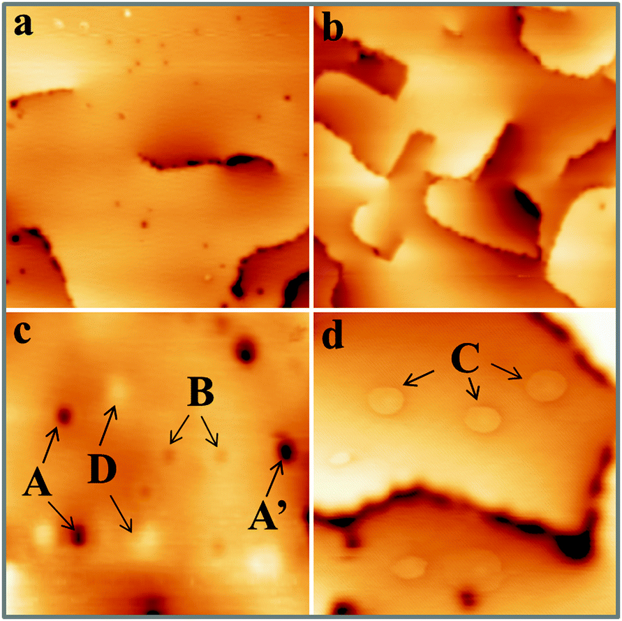 | ||
| Fig. 1 STM topographic images of two 30 ML thick CaO films annealed to (a) 1200 K and (b) 1000 K (500 × 500 Å2). Note the different defect concentrations. (c and d) High resolution images showing the four different defect types discussed in the text (200 × 200 Å2). | ||
The first intrinsic lattice defect discussed here is a round depression of 0.8 Å depth and 7–10 Å diameter, values that hardly change with the bias and current set-point for imaging (Fig. 2a). This defect, denoted as A-type, is primarily found on highly doped CaOMo films and its abundance increases sharply with sample annealing. The defect mostly appears as isolated species, but can agglomerate also to larger clusters, as marked with A′ in Fig. 1c. Also the next defect, called B-type, shows up as a depression in the STM images (Fig. 2b). Its depth is considerably reduced with respect to the A-defect (0.4 Å). In addition, B-defects are surrounded by one, sometimes two concentric rings of 15 and 40 Å diameter, respectively. No changes in ring size are observed in the broad bias window from 2.5 to 5.5 V. The density of B-defects seems to be connected to the one of A-defects, as both features become more abundant upon high-temperature annealing. However, the absolute number of A-defects always exceeds the one of B-defects by almost one order of magnitude.
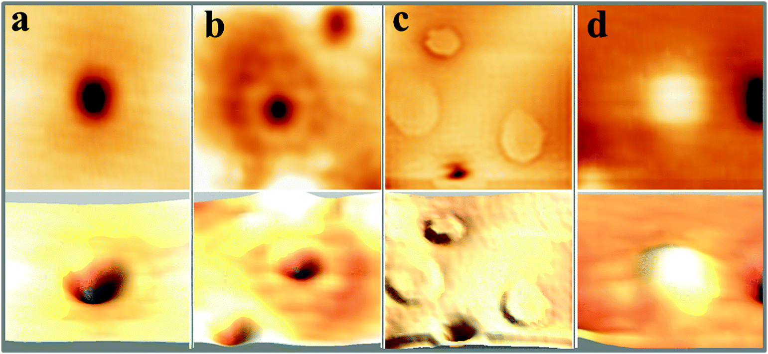 | ||
| Fig. 2 Close-up images of the four typical defects on the surface of CaOMo films (a, b and d: 50 × 50 Å2, c: 100 × 100 Å2). (a) Minimum of 0.8 Å depth (A-defect). (b) Shallow depression surrounded by concentric rings (B-defect). (c) Ring features with up to 50 Å diameters (C-defect) and (d) shallow protrusions of 0.15 Å height (D-defect). Top and bottom images are 2D and pseudo 3D representations of the same defect type. | ||
Also the third defect (C-type) shows up as characteristic ring feature; however, the rings are much larger and may reach up to 50 Å diameter on the CaO surface (Fig. 1d). In contrast to B-defects, the ring size sensitively depends on the film thickness and the bias voltage in this case. Whereas an enlargement of the ring diameter is observed on thicker films, the ring size exhibits a minimum at 4 V and grows with decreasing or increasing bias voltage. Another difference to A and B-defects is the absence of a maximum or minimum in the ring center. Finally, Gaussian protrusions of different height can be observed on the CaOMo films, the D-defects. The fainter maxima are as small as 0.15 Å, while the larger ones reach a maximum height of 1.0 Å. A selection of the main topographic defects found on the CaOMo surface is presented in Fig. 2, both in 2D and pseudo 3D representation for better visibility. Most of these defects were detected on flat oxide terraces and not along step edges and dislocation lines. We assume, however, that this distribution is somewhat artificial and mainly governed by experimental difficulties to identify faint irregularities next to a highly corrugated defect line. Moreover, the different defect types coexist in one and the same surface region. In particular, type A and C defects are often found together with a mutual separation of less than 25 Å (Fig. 3).
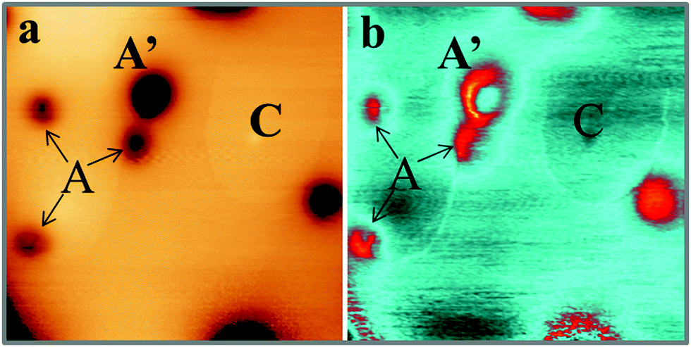 | ||
| Fig. 3 (a) STM topographic and (b) corresponding dI/dV image of a 30 ML thick CaO film. Note the spatial proximity between the A and C defects. The latter is best seen in the conductance image due to its small apparent height (200 × 200 Å2). | ||
3.2. Identification of point defects in CaOMo
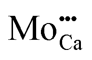
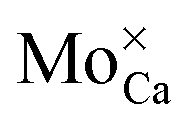
An assignment of the different features observed on the CaOMo surface to real point defects is difficult with ab initio methods. Although DFT calculations safely predict the ground-state properties and thermodynamic stability of oxide defects, simulation of the respective STM images is not always conclusive due to the unknown tip conditions and deficiencies of the Tersoff–Hamann approach to describe image formation on gap materials. We therefore use plausibility considerations and input from earlier calculations to connect the experimentally observed features to defects in the oxide lattice.10,18,29The following defects need to be considered in our system: Mo dopants, compensating cationic vacancies and oxygen vacancies, as the fundamental oxide defect. The Mo ions are expected to substitute Ca2+ species in the rocksalt lattice and might be present in different charge states that are in a Kröger–Vink notation:  .30 While the first one is isovalent with the substituted Ca2+ ion, the latter two carry a positive net charge. According to DFT calculations,29 higher oxidation states are systematically preferred from an energy point of view, as this removes high-lying electrons from energy levels in the band gap. The release of Mo electrons requires however the presence of suitable acceptor states, which are provided by Ca vacancies (
 )18 or suitable line defects.31,32 Each Ca vacancy produces two hole-states in the oxygen-derived valence band, which are able to trap two electrons from adjacent Mo donors. The efficiency of such internal compensation scheme becomes evident from the calculated formation energy of VCa centers. Whereas Ca vacancy formation costs 8 eV in pristine CaO, this value drops to 1.5 eV in the Mo doped material.18 Charged Ca vacancies, the
  centers, can occur if one or two extra electrons get trapped in the O 2p hole-states generated by the neutral vacancy. Finally, oxygen vacancies with different charge state (
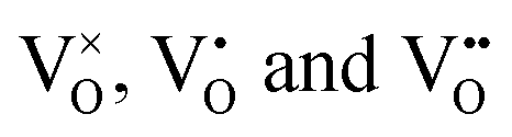 defects) might be present in the oxide lattice. The easiness to produce VO defects in CaO controls the abundance of Ca vacancies and, in turn, the charge state of the Mo dopants. In general, preparation at O2-poor conditions promotes the development of O vacancies, which sets a thermodynamic hindrance for simultaneous insertion of Ca defects. Conversely, preparation at high O2 chemical potential favors the development of compensating Ca holes, pushing the Mo ions to higher oxidation states. Note that the simultaneous development of cationic and anionic vacancies is considered to be unlikely from an energetic point of view.16
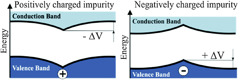
On the basis of these thermodynamic considerations, the preparation conditions realized in the experiment and the morphological fingerprints seen in STM, we now propose the following assignment of the experimental features A–D to lattice defects in CaOMo. The ring-like C-feature is connected to the charging signature of single subsurface Mo2+ ions in the electric field of the STM tip, as already discussed in an earlier paper.25 Upon scanning with a negatively biased tip, the oxide electronic states experience an upshift that may lead to a temporary ionization of the Mo ions in the near surface region of the oxide. The charge transfer from the localized Mo orbitals into the CaO conduction band becomes feasible, as the dopant HOMO locates only 1.5 eV below the band onset, an energy difference that is easily overcome via tip-induced band bending. The hence positively charged Mo ion (a 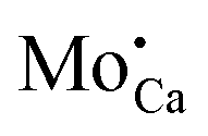 defect) generates an attractive Coulomb potential around the defect that locally increases the available LDOS for electron tunneling from the tip.24,33 As a result, a bright circular region shows up around the dopant, being associated to the C-defect. The size of the charging ring is given by the maximum distance at which the tip is still able to ionize the Mo donor. It therefore depends on the thickness of the film, its dielectric response, and the applied bias voltage that controls the band bending. The charging rings occur only for Mo ions in low oxidation states, while Mo4+ and Mo5+ species cannot be oxidized in the tip electric field as their HOMO levels are too deep in the band gap.25
We continue our discussion with the A-defect that shows up as plain hole in the CaO surface over the entire experimental bias window (Fig. 2a). The defect is assigned to an empty Ca vacancy (a 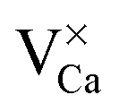 center). It appears with negative contrast in the STM, because it is a simple void in the top-most CaO plane from a structural point of view, and does not introduce new electronic states into the gap region that would enhance the tunneling probability.18 Note that a similar conclusion has been drawn from earlier experiments on Cr-doped MgO films, where circular depressions in the MgO surface have been related to the compensating Mg-vacancies and not to the Cr dopants.34 Also the B-defects are associated with Ca vacancies, although they appear with reduced contrast and feature a characteristic sombrero shape. We propose that these vacancies are either located in a subsurface plane or hold extra electrons from adjacent Mo donors, converting them into
 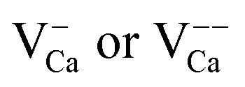 centers. The deviating charge state with respect to an intrinsic Ca2+ ion leads to a screened Coulomb potential around the defect:
 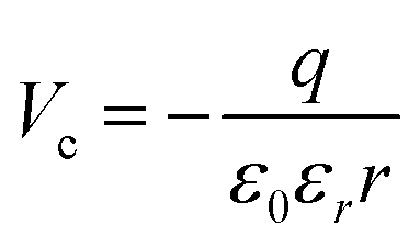 that serves as scattering center for electrons and may express bound electronic states.35 Both effects might be responsible for the development of concentric rings around the B-defect, hence its characteristic sombrero shape.37 From STM images, as the one shown in Fig. 3, we deduce a certain spatial proximity between A (sometimes B) and C defects, reflecting the mutual stabilization between a donor species and its compensating cationic vacancy.13,18 However, our data base is not sufficient for a statistical evaluation of the mean A–C distances and we therefore refrain from a discussion of interaction energies.
Identification of the D defects (Fig. 2d) is ambiguous; however an assignment to different adsorbates seems plausible. Both CO2 and H2O are known to interact strongly with CaO and may spontaneously bind to the surface even at ideal vacuum conditions.36 Also, the formation of molybdyl species (Mo![[double bond, length as m-dash]](https://www.rsc.org/images/entities/char_e001.gif) O) from Mo ions in the topmost oxide layer is possible. A clear assignment would require more systematic adsorption studies and is beyond the scope of this paper.
O) from Mo ions in the topmost oxide layer is possible. A clear assignment would require more systematic adsorption studies and is beyond the scope of this paper.
Finally, we want to explain why O vacancies have been disregarded in our interpretation. As discussed before, the CaOMo film features strong electron-donor behavior and excess electrons are abundant in the lattice. Neutral oxygen vacancies ( ) act as electron donors as well, as they are able to transfer up to two electrons to suitable trap sites.13 The development of O defects in the oxide is therefore energetically unfavorable and would push the charge balance further to the electron-rich side. Moreover, the observed point defects are not compatible with the signature of oxygen vacancies that have been described in detail for MgO thin films.37 In the next chapter, we discuss the impact of the different point and line defects on the local electronic structure of the oxide film.
3.3. Electronic fingerprints of defects in CaOMo films
CaO, as a wide-gap insulator of 7.1 eV band gap, has a rather simple electronic structure that consists of a Ca 3s type conduction and an O 2p type valence band. The Mo impurities alter this structure by shifting the energy position of the CaO bands and introducing localized states into the band gap. As the dopant concentration is not homogenous in the oxide matrix, the electronic properties will display spatial modulations both vertical and parallel to the surface. Three energy windows are of interest in an STM experiment that deals with Mo dopants in a CaO matrix, (i) the gap region, (ii) the onsets of the CaO bulk bands and (iii) the vacuum states above the surface. While the gap region includes the 4d levels of the Mo dopants,10 the band onsets carry information on band-bending effects due to excess charges in the film.38 Finally, the vacuum states may be explored to deduce the influence of Mo donors on the CaO(001) surface potential.39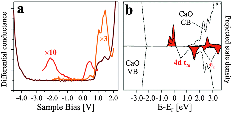 | ||
| Fig. 4 (a) Conductance spectrum and (b) calculated LDOS (PBE) of CaOMo films. The experimental curves have been taken at different bias set-points: dark red curve: +2.0 V, red and orange curve +1.0 V. The eg and t2g contributions to the Mo 4d states are clearly distinguishable in experimental as well as calculated spectra. The calculations refer to a Mo3+ dopant in a subsurface position. | ||
The distribution of Mo dopants in the CaO lattice is not expected to be homogenous, which gives rise to spatial modulations in the electronic structure. Topographic STM images hardly reveal such effects, as they integrate over electronic states in a wide bias window; however dI/dV maps may provide energy-dependent information on the electron transport channels. This is demonstrated in Fig. 5, which shows in (a) the smooth surface morphology of 15 ML CaOMo with a small number of cationic vacancies (A-defects), and in (b) the respective dI/dV maps that exhibit a surprisingly large contrast. As a function of the bias voltage, regions with high and low dI/dV signal alternate on the surface and produce an irregular pattern with 30–50 Å structure size. Whereas for some bias values, a correlation with the defect morphology is evident, no relation between dI/dV contrast and defect landscape is revealed for others. The A-defects, for example, introduce areas of high conductance at 0.8–1.0 V sample bias, while no obvious contrast is detected in maps taken below 0.5 V. A possible explanation for this variability is the occurrence of ‘hidden’ conductance channels, introduced by bulk or surface defects that do not leave topographic fingerprints in the STM images. In fact, we expect an enhanced dI/dV signal in regions that contain a large number of Mo dopants with 4d levels matching the preset sample bias. Conversely, low dI/dV contrast prevails when either the density of dopants is low or their level energy does not overlap with the imaging bias. This interrelation between structure and electronic properties is the likely reason for the highly corrugated dI/dV maps taken at bias voltages inside the CaO band gap.
 | ||
| Fig. 5 (a) STM topographic image and (b) corresponding dI/dV maps taken on 15 ML thick CaOMo films at the indicated bias voltages (200 × 200 Å2). The inhomogeneity of the electronic structure reflects the uneven spatial distribution of Mo ions inside the oxide lattice. | ||
Although individual donors cannot be identified, the dI/dV maps of Fig. 5b suggest an agglomeration of Mo impurities and/or compensating defects in certain regions of the CaO lattice. A clustering of impurities and defects has been observed for other oxides before, for instance for V2O338 and Li-doped silica.40 Driving force for such effects might be the minimization of lattice strain, e.g. by isolating defect-poor and defect-rich areas. We emphasize at this point that defect-clustering affects not only the electronic structure but also the local adsorption and reactivity behavior of the doped oxides.
A set of dI/dV spectra taken on defect-free CaO terraces and Ca vacancies is shown in Fig. 6a. Although the true band onset is difficult to fix due to the unknown impact of gap states and tip-induced band bending, the fundamental conductance rise clearly occurs at different bias values. It is first observed on the defect-free CaO film, where a conductance step is detected at ∼1.3 V, but shifts upward by a few 100 mV on cation vacancies and vacancy clusters (A and B defects). The opposite trend is revealed for C-defects and CaO dislocation lines, being the dominant defect type in the dI/dV maps of Fig. 6c and d. Those sites turn bright at bias voltages that are lower than the conductivity onset on the ideal surface, suggesting a local downshift of the conduction band. Again, substantial spatial modulations are identified for the band onset, reflecting the in-homogeneous electronic structure of the CaOMo films.
 | ||
| Fig. 6 (a) STM topographic image of a 15 ML CaOMo film (200 × 200 Å2) and (b) dI/dV spectra taken at the indicated surface positions. The setpoint bias was set to 2.0 V in all four cases. (c and d) Topographic image and corresponding dI/dV map taken at 3.5 V on a 30 ML thick CaOMo film (450 × 450 Å2). The most prominent defects in the image are the Mo dopants (C-defects) and the dislocation lines. | ||
The presence of excess charges in the oxide lattice offers an explanation for local shifts of the band onsets. Cation vacancies (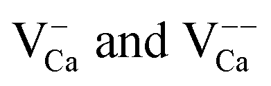 ) are negatively charged with respect to the ideal lattice. The negative potential induces a local upshift of the bands around these defects, as observed in the dI/dV spectra of Fig. 6b. In contrast, highly oxidized Mo species carry positive excess charges, which generate an attractive electron potential and lead to a downshift of the oxide bands. A similar behavior is revealed for the line defects that display enhanced dI/dV contrast below the band onset of the flat film (Fig. 6c and d). The contrast increase indicates downward bending of the conduction band at the dislocation lines, for instance due to clustering of positively charged
  centers. The agglomeration effect might be the consequence of strain reduction in the oxide lattice when the dopants move into less organized defect regions. In addition, the dislocations serve as diffusion channels for Mo ions from the support.27 It is worth noting that line defects in non-doped MgO films behave as electron traps and are negatively charged, which is the reason for their reduced contrast in the dI/dV maps.32
Our rationalization has been confirmed by DFT calculations. To analyze the observed band bending in the proximity of charged defects, we have computed core level shifts of surface Ca atoms as a function of their distance from the defect. In fact, the core-level shifts arise from the same change in the electron potential that is responsible for bending the oxide bands. Calculated shifts for the expected defects are summarized in the Table 1. In full agreement with the experiments, a substitutional Mo ion induces a downshift of the oxide electronic states, while the levels move upwards in presence of negatively charged 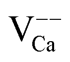 centers.
| Defect | Band bending [eV] | |
|---|---|---|
 (Mo3+ subsurface) (Mo3+ subsurface) |
−0.09 |
|
 (Mo4+ subsurface) (Mo4+ subsurface) |
−0.29 | |
 (Mo5+ subsurface) (Mo5+ subsurface) |
−0.49 | |
 (Mo2+ surface) (Mo2+ surface) |
−0.14 | |
| MoO (Mo4+ surface) |
−0.18 | |
 (surface) (surface) |
−0.23 | |
 (surface) (surface) |
+0.45 |
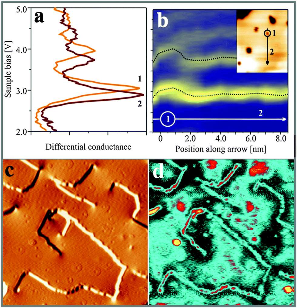 | ||
| Fig. 7 (a) High-bias conductance spectra taken on 15 ML CaOMo with enabled feed-back loop. The two surface positions for spectroscopy are marked in the topographic image on the right (180 × 150 Å2). (b) Series of 20 FER spectra taken along the black line in the topographic image. In both data sets, the FERs exhibit an energy shift when the tip approaches a cationic vacancy. The behavior is compatible with a formally negative charge of the surface defect. (c and d) Topographic image and corresponding dI/dV map taken at 4.6 V on a 30 ML thick CaOMo film (450 × 450 Å2). | ||
Fig. 7a shows two high-energy spectra taken on top of a Ca vacancy (A-defect, orange line) and on the bare film (red line). In both cases, the characteristic sequence of FERs is observed; however, the peak positions on the defect site are clearly upshifted. The spatial dependence of the FER-energies is visualized in a spectral series taken across a single Ca vacancy (Fig. 7b, line in the inset). The 20 spectra are plotted in a matrix representation with the dI/dV intensity coded in color (blue: low dI/dV signal). The 1st to 3rd FERs are clearly resolved as bright, horizontal lines that get perturbed when the tip enters a 1 nm-circle around the defect. As revealed for the point spectra, the resonances experience an upshift in the vicinity of Ca vacancies, indicative for a local increase of the surface potential Φ. Such a potential increase would be compatible with a formal negative charge of the VCa centers, as discussed before. The opposite trend is revealed for CaO surfaces with an abundance of Mo-donors (C-defects). In the respective dI/dV maps taken in the field emission regime, the C-defects turn bright clearly before the pristine film (Fig. 7c and d). Apparently, the first FER becomes available for electron transport already at bias values that are lower than on the bare surface. The same effect is observed for the CaO dislocation lines that are also imaged with enhanced dI/dV contrast. Both observations are in line with the anticipated downshift of the vacuum states above positively charged Mo centers, and also corroborate the idea that Mo ions get enriched along the CaO line defects.
4. Summary
Using scanning tunneling microscopy and spectroscopy, different point and line defects have been identified in crystalline CaO films doped with high-valence Mo ions. The dopants show up as extended charging rings that arise from a reversible switching of their oxidation state in the tip-electric field. The charge switching is possible only for Mo2+ ions in a near-surface region, while higher oxidized or bulk-like species are resistant against tip-induced perturbations. Ca vacancies, being the compensating defects for the Mo donors, are imaged as deep holes in the CaO surface. According to DFT calculations, this defect type has low formation energy in CaOMo films, as it provides trap states for the extra electrons from the Mo donors. Differential conductance spectra corroborate the proposed assignment of the point defects. The Mo dopants feature a set of 4d-related gap states that exhibit the expected splitting into a low-lying t2g and a high-lying eg manifold. Charged defects are identified via their long-ranged Coulomb response onto the surrounding oxide. The Ca vacancies carry a formally negative charge that gives rise to an upshift of the CaO conduction band and the vacuum states in their vicinity. In contrast, the Mo dopants and most of the line defects are positively charged and stabilize the oxide electronic states.The main result of our experiment is the surprisingly large inhomogeneity of the oxide electronic structure. In contrast to non-doped films, the absolute band position, the overall gap width and the abundance of localized defect states in the gap feature pronounced spatial variations that might be explained with an agglomeration of dopants and compensating defects in certain oxide regions. We expect that this inhomogeneity strongly affects the adsorption behavior and the chemical properties of doped oxides. Charge transfer into suitable adsorbates, for example, might preferentially occur in regions with high dopant concentration, e.g. along the oxide line defects. Our STM technique is ideally suited to probe the defect landscape with high spatial resolution and enables a detailed analysis of charge centers and their impact on the chemical properties of doped oxides.
Acknowledgements
This work was supported by the DFG Excellence Project ‘UNICAT’, and the FIRB Project RBAP115AYN. We also thank the COST Action CM1104. Y. C. is grateful for a fellowship of the Humboldt Foundation.References
- E. W. McFarland and H. Metiu, Chem. Rev., 2013, 113, 4391–4427 CrossRef CAS PubMed.
- H.-J. Freund, M. Heyde, N. Nilius, S. Schauermann, S. Shaikhutdinov and M. Sterrer, J. Catal., 2013, 308, 154–167 CrossRef CAS PubMed.
- A. Janotti and C. G. Van de Walle, Rep. Prog. Phys., 2009, 72, 126501 CrossRef.
- A. Corma, P. Atienzar, H. Garcia and J. Y. Chane-Ching, Nat. Mater., 2004, 3, 394–397 CrossRef CAS PubMed.
- H. Y. Kim, H. M. Lee, R. G. S. Pala, V. Shapovalov and H. Metiu, J. Phys. Chem. C, 2008, 112, 12398–12408 CAS.
- J. Andersin, J. Nevalaita, K. Honkala and H. Häkkinen, Angew. Chem., Int. Ed., 2013, 52, 1424–1427 CrossRef CAS PubMed.
- X. Sun, B. Li and H. Metiu, J. Phys. Chem. C, 2013, 117, 7114–7122 CAS.
- X. Shao, N. Nilius and H. J. Freund, J. Am. Chem. Soc., 2012, 134, 2532–2534 CrossRef CAS PubMed.
- M. Nolan, J. Phys. Chem. C, 2009, 113, 2425–2432 CAS.
- X. Shao, S. Prada, L. Giordano, G. Pacchioni, N. Nilius and H. J. Freund, Angew. Chem., Int. Ed., 2011, 50, 11525–11527 CrossRef CAS PubMed.
- Y. Cui, X. Shao, M. Baldofski, J. Sauer, N. Nilius and H.-J. Freund, Angew. Chem., Int. Ed., 2013, 52, 11385–11387 CrossRef CAS PubMed.
- J. X. Wang and J. H. Lunsford, J. Phys. Chem., 1986, 90, 5883–5887 CrossRef CAS.
- P. Myrach, N. Nilius, S. V. Levchenko, A. Gonchar, T. Risse, K. P. Dinse, L. A. Boatner, W. Frandsen, R. Horn, H. J. Freund, R. Schlogl and M. Scheffler, ChemCatChem, 2010, 2, 854–862 CrossRef CAS.
- R. Asahi, T. Morikawa, T. Ohwaki, K. Aoki and Y. Taga, Science, 2001, 293, 269–271 CrossRef CAS PubMed.
- C. Di Valentin, E. Finazzi, G. Pacchioni, A. Selloni, S. Livraghi, M. C. Paganini and E. Giamello, Chem. Phys., 2007, 339, 44–56 CrossRef CAS PubMed.
- J. Robertson and S. J. Clark, Phys. Rev. B: Condens. Matter Mater. Phys., 2011, 83, 075205 CrossRef.
- Z. P. Hu, B. Li, X. Y. Sun and H. Metiu, J. Phys. Chem. C, 2011, 115, 3065–3074 CAS.
- F. Stavale, X. Shao, N. Nilius, H. J. Freund, S. Prada, L. Giordano and G. Pacchioni, J. Am. Chem. Soc., 2012, 134, 11380–11383 CrossRef CAS PubMed.
- N. A. Richter, F. Stavale, S. V. Levchenko, N. Nilius, H. J. Freund and M. Scheffler, submitted.
- B. Henderson and G. F. Imbusch, Optical Spectroscopy of Inorganic Solids, Oxford, Clarendon, 1989 Search PubMed.
- K. Teichmann, M. Wenderoth, S. Loth, R. G. Ulbrich, J. K. Garleff, A. P. Wijnheijmer and P. M. Koenraad, Phys. Rev. Lett., 2008, 101, 076103 CrossRef CAS.
- P. M. Koenraad and M. E. Flatte, Nat. Mater., 2011, 10, 91–100 CrossRef CAS PubMed.
- M. Batzill, K. Katsiev, D. J. Gaspar and U. Diebold, Phys. Rev. B: Condens. Matter Mater. Phys., 2002, 66, 235401 CrossRef.
- H. Zheng, J. Kroger and R. Berndt, Phys. Rev. Lett., 2012, 108, 076801–076805 CrossRef; H. Zheng, A. Weismann and R. Berndt, Phys. Rev. Lett., 2013, 110, 226101–226104 CrossRef.
- Y. Cui, N. Nilius, H.-J. Freund, S. Prada, L. Giordano and G. Pacchioni, Phys. Rev. B: Condens. Matter Mater. Phys., 2013, 88, 205421 CrossRef.
- X. Shao, P. Myrach, N. Nilius and H. J. Freund, J. Phys. Chem. C, 2011, 115, 8784–8789 CAS.
- X. Shao, N. Nilius, P. Myrach, H. J. Freund, U. Martinez, S. Prada, L. Giordano and G. Pacchioni, Phys. Rev. B: Condens. Matter Mater. Phys., 2011, 83, 245407 CrossRef.
- N. Nilius, Surf. Sci. Rep., 2009, 64, 595–659 CrossRef CAS PubMed.
- S. Prada, L. Giordano and G. Pacchioni, J. Phys. Chem. C, 2013, 117, 9943–9951 CAS.
- F. A. Kröger and H. J. Vink, Solid State Phys., 1956, 3, 307–435 Search PubMed.
- K. P. McKenna and A. L. Shluger, Nat. Mater., 2008, 7, 859–862 CrossRef CAS PubMed.
- H. M. Benia, P. Myrach, A. Gonchar, T. Risse, N. Nilius and H. J. Freund, Phys. Rev. B: Condens. Matter Mater. Phys., 2010, 81, 241415 CrossRef.
- G. V. Nazin, X. H. Qiu and W. Ho, Phys. Rev. Lett., 2005, 95, 166103 CrossRef CAS.
- F. Stavale, N. Nilius and H. J. Freund, New J. Phys., 2012, 14, 033006 CrossRef.
- R. J. Hamers, J. Vac. Sci. Technol., B, 1988, 6, 1462–1467 CAS.
- D. Ochs, B. Braun, W. Maus-Friedrichs and V. Kempter, Surf. Sci., 1998, 417, 406–414 CrossRef CAS.
- M. Sterrer, M. Heyde, M. Novicki, N. Nilius, T. Risse, H. P. Rust, G. Pacchioni and H. J. Freund, J. Phys. Chem. B, 2006, 110, 46–49 CrossRef CAS PubMed.
- V. Simic-Milosevic, N. Nilius, H. P. Rust and H. J. Freund, Phys. Rev. B: Condens. Matter Mater. Phys., 2008, 77, 125112 CrossRef.
- E. D. L. Rienks, N. Nilius, H. P. Rust and H. J. Freund, Phys. Rev. B: Condens. Matter Mater. Phys., 2005, 71, 241404 CrossRef.
- J. F. Jerratsch, N. Nilius, H. J. Freund, U. Martinez, L. Giordano and G. Pacchioni, Phys. Rev. B: Condens. Matter Mater. Phys., 2009, 80, 245423 CrossRef.
- W. Mönch, Semiconductor Surfaces and Interfaces, Springer, 1993 Search PubMed.
- R. M. Feenstra, Phys. Rev. B: Condens. Matter Mater. Phys., 1994, 50, 4561–4570 CrossRef CAS; G. J. de Raad, D. M. Bruls, P. M. Koenraad and J. H. Wolter, Phys. Rev. B: Condens. Matter Mater. Phys., 2002, 66, 195306 CrossRef.
- G. Binnig, K. H. Frank, H. Fuchs, N. Garcia, B. Reihl, H. Rohrer, F. Salvan and A. R. Williams, Phys. Rev. Lett., 1985, 55, 991–994 CrossRef CAS.
- O. Y. Kolesnychenko, Y. A. Kolesnichenko, O. Shklyarevskii and H. van Kempen, Physica B, 2000, 291, 246–255 CrossRef CAS.
| This journal is © the Owner Societies 2014 |