Nanorod assisted lateral epitaxial overgrowth of ZnO films in water at 90 °C
H. Q.
Le
,
G. K. L.
Goh
* and
L.-L.
Liew
Institute of Materials Research and Engineering, A*STAR (Agency for Science, Technology, and Research), 3 Research Link, 117602 Singapore, Singapore. E-mail: g-goh@imre.a-star.edu.sg
First published on 25th October 2013
Abstract
A novel method was used to grow epitaxial ZnO films by employing a nanorod assisted lateral epitaxial overgrowth process at a low growth temperature of 90 °C in water utilizing a continuous circulation reactor. The relatively smooth films had an epitaxial relationship with the sapphire substrate, as confirmed by off-axis φ scans. Films grown for 72 hours had a high carrier concentration of 3.12 × 1018 cm−3 and mobility of 9.75 cm2 V−1 s−1 after thermal treatment at 300 °C. The threading dislocation density of the thickest film was 5 × 108 cm−2, 2 orders of magnitude lower than that of normal solution grown ZnO films.
1. Introduction
Growth of highly crystalline ZnO films has attracted a lot of research activity due to their potential as an alternative to the established GaN and Si based solid state lighting and thin film transistor devices.1–4 ZnO has been considered as a cost effective material with simple synthesis processes. Meanwhile, GaN-based devices involve complicated and expensive fabrication processes and free standing GaN substrates still need to be used despite their high cost and cracking related mechanical degradation. As a result, ZnO is a suitable alternative candidate to GaN to reduce the fabrication cost and the realization of larger sizes. Besides, ZnO thin films also exhibit high transparency and excellent conductivity.ZnO and GaN share many similar properties such as crystal structure, band gap and lattice constant. Growing ZnO epitaxial layers with low defect density on sapphire is a key requirement for use in high efficiency optical and electronic devices. Usually, ZnO grown on sapphire has high dislocation densities due to large lattice constant and high thermal expansion coefficient mismatches. The lateral epitaxial overgrowth method has been successfully applied to GaN5 and ZnO6 film growth to reduce dislocation density. However, this technique also has some drawbacks such as the requirement for masks and complicated lithography processes which increase the fabrication cost and hinder mass production. The nanorod-assisted lateral epitaxial overgrowth method was proposed in order to grow thick single crystalline ZnO films with relatively low dislocation density by a solution method7 and by MOCVD.8 However, the latter method required processing temperatures of 420 °C and the use of more expensive MOCVD equipment and did not give any quantitative values for what it called ‘low dislocation densities’.
Currently, growth of ZnO films has been widely reported using vapor phase methods including molecular beam epitaxy (MBE),9,10 metal organic chemical vapor deposition (MOCVD),11 pulsed laser deposition (PLD)12,13 and the hydrothermal method.14,15 Of the many techniques used for ZnO film growth, the hydrothermal method used to grow films is the low temperature variant also known as chemical bath deposition when growth temperatures below the boiling point of water are employed. It has been used to synthesize powders and nanostructures in addition to dye sensitized solar cells and opto-electronic films.16,17
While high temperature hydrothermal growth of ZnO has become a standard method for producing large single crystals,18–20 low temperature aqueous synthesis (e.g. chemical bath deposition) has become an especially attractive method for producing ZnO due to its advantages of having lower capital and operating costs and also less significant environmental impact.21 Recognizing this, Richardson and Lange22,24 designed and demonstrated a continuous circulation reactor based on the fact that ammonia can form stable zinc complexes in solution. Relying on standard thermodynamic data, equilibrium calculations showed that the solubility of ZnO at room temperature can be significantly increased with the addition of ammonia. It was noticed that this solubility decreased with increasing temperature i.e. retrograde solubility. Based on these calculations, a reactor was built in which an excess of ZnO powder is contained in the dissolution vessel, maintained at room temperature and filled with an aqueous ammonia solution. This led to the development of a solution continuously saturated with soluble zinc species. This solution was then pumped to the deposition vessel maintained at a higher temperature which caused ZnO to precipitate due to the reduced solubility. Any ZnO not used in the growth of the ZnO on the selected substrate in the deposition vessel is pumped back to the dissolution vessel to be dissolved and re-used.
Here we report a maskless nanorod assisted lateral epitaxial overgrowth (nanorod LEO) method to grow ZnO films in water at the low temperature of 90 °C. The lateral epitaxial overgrowth was carried out in a continuous circulation reactor which maximizes precursor material and has the potential for growth of thick films without the need to refresh the precursor solution which in turn reduces the risk of contamination. Therefore, it offers great potential for use in the actual fabrication of ZnO substrates and devices.
2. Experimental
Prior to ZnO film growth, a ZnO nanorod array was formed on c plane sapphire substrates by a modification of a process first developed by Li et al.24 Firstly, the substrate was alternately dipped in zinc acetate dehydrate and ethanol solutions followed by heating at 300 °C for 30 min to form a thin crystalline ZnO layer.25 The coated substrates were then heated at 1000 °C for 1 hour to form an epitaxial ZnAl2O4 buffer layer. Any residual ZnO was removed with diluted HCl solution. ZnO nanorod arrays were then grown onto the substrate by immersing in a solution of zinc nitrate hexahydrate (25 mM Zn(NO3)2·6H2O, 98%) and 25 mM of hexamethylenetetramine (HMT) at 95 °C. These steps are illustrated in Fig. 1. | ||
| Fig. 1 Process flow for the growth of ZnO films on the sapphire substrate. | ||
ZnO films were then grown by lateral epitaxial overgrowth of each nanorod in the deposition vessel of a continuous circulation reactor that makes use of the retrograde solubility of ZnO in ammonia solutions. The ZnO saturated ammonia solution for the ZnO film growth was prepared by first dissolving 0.5 M NH3 solution (25%) and 14 mM sodium citrate in distilled water. Sodium citrate was added to enhance the lateral growth of ZnO crystals. Then, the solution was saturated with soluble zinc species with an excess amount of ZnO powder added to the dissolution vessel. HNO3 acid was then added into the solution to adjust its pH value to 11.
For chemical bath deposition, the precursor concentrations, growth time, growth temperature and pH are the main control parameters affecting not only the morphology but also the properties of the synthesized films. In this work, only the growth time was varied while the concentration of the soluble chemical precursors and pH did not change appreciably during growth as ZnO powders were used in excess to keep the growth solution saturated.
A schematic of the continuous circulation reactor used for film growth is shown in Fig. 2. The reactor consists of two plastic vessels. The deposition vessel was heated by a coiled tape to 90 °C while the dissolution vessel was kept at room temperature. The ammonia solution was circulated within the two vessels by a peristaltic pump at a very slow flow rate (<5 mL min−1) while the excess ZnO powder in the cooler dissolution vessel kept the concentration of Zn ions constant. The substrates for film growth were placed upside down in a Teflon holder in the hot deposition vessel and growth was performed for various growth times (from 24 to 168 hours).
 | ||
| Fig. 2 Continuous circulation reactor setup used in the experiment to synthesize ZnO films on sapphire. | ||
After growth, the morphology and microstructure of the films were studied by field emission scanning electron microscopy (FESEM 6700F) and X-ray diffractometry (X'Pert High Resolution XRD Systems). Photoluminescence spectra of the films were recorded with a Renishaw 2000 micro PL set up. The 325 nm line of the He–Cd laser was used as a source of excitation. Carbolite Box Furnace CWF1100 was used to heat-treat the samples. The electrical properties of the ZnO films were measured by a Hall measurement system (HL5500) employing the van der Pauw method. The threading dislocation density of the epitaxial films was determined by a surface etching method: etching the Zn-terminated (0001) surface at room temperature for 30–40 s using a 1% diluted acetic acid.26
3. Results and discussion
In order to attain well aligned ZnO nanorods on sapphire substrates, Li et al.24 showed that an epitaxial ZnAl2O4 buffer layer is required. This buffer layer was formed by a solid state reaction between the sapphire substrate and a thin ZnO seed layer during heat treatment at high temperature (>800 °C). It is known that ZnAl2O4 has the same crystal structure as MgAl2O4 and a similar lattice parameter (8.0867 Å vs. 8.083 Å) and that MgAl2O4 has been used successfully as a template to grow epitaxial ZnO nanorods and films.26,27 Therefore, a similar epitaxial relationship is expected for ZnO growth on ZnAl2O4.Bare sapphire surfaces do not provide suitable epitaxial nucleation sites for ZnO nanostructure growth under solution conditions (see randomly oriented rods in Fig. 3a). Fig. 3b shows ZnO nanorod growth on a sapphire surface with the ZnAl2O4 buffer layer. The nanorods were highly aligned with a well defined hexagonal shape, an average height of 2 μm and a diameter of 100 nm. According to Li et al.,24 rods grown by this method are epitaxially related to the sapphire substrate due to the small lattice mismatch between (0001) ZnO and (111) ZnAl2O4 (~1.6%).
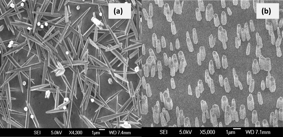 | ||
| Fig. 3 Morphology of ZnO nanorods grown on (a) bare sapphire substrate and (b) sapphire surface with buffer layer. | ||
A continuous circulation reactor was used to offer a steady growth condition to produce epitaxial films with various thicknesses. This continuous reactor takes advantages of the retrograde solubility of ZnO with temperature in aqueous ammonia solutions. Unlike normal chemical bath deposition, the concentration of the chemical precursors and pH do not change appreciably during growth. As a result, highly uniform ZnO films at constant growth rate can be obtained. In detail, the main reactions showing the principle operation of the continuous reactor are described in the following paragraph.
At the cold zone (room temperature), where there is an excess of ZnO powder, ZnO was dissolved according to:
| ZnO + 4NH3 + 2H+ → Zn(NH3)42+ + H2O | (1) |
In the report by Richardson and Lange,23 a growth rate normal to the substrate of ~0.8 μm h−1 was recorded. In the present study, a growth rate of ~0.1 μm h−1 was observed, as shown by the graph in Fig. 4. This large decrease in growth rate is not unexpected since sodium citrate was added in the growth solution in this study. As reported in ref. 6, the triply negatively charged citrate ion preferentially adsorbs to the ZnO c face, slowing growth on this face and in this way promotes growth on the other faces, namely lateral film growth.
 | ||
| Fig. 4 Dependence of film's thickness and morphology on growth time. | ||
Fig. 4 also shows the effect of growth time on film morphology using the continuous circulation reactor. At short growth time (24 hours), 3–5 μm sized hexagonal shaped islands could be clearly observed. These hexagonal disks indicated that the islands were actually the aligned rods seen in Fig. 3b that had enlarged by lateral growth. Continuous lateral overgrowth of the initial rods leads to coalescence into an almost continuous film (notice the pores between some islands). It was noticed that a not small number of the edges of the hexagonal islands were not parallel with each other, suggesting that a number of the ZnO rods grown on the ZnAl2O4 buffer layer were not exactly epitaxial. With longer growth time (72 hours), these islands continued to enlarge, coalesce and produce a fully coalesced film with a much smoother surface morphology and a thickness of ~9 μm. The edges of the hexagonal islands were not very visible and the faint edges that could be observed are mostly parallel.
The epitaxial relationship between the overgrown ZnO film and substrate was studied by X-ray diffraction in Fig. 5 by measuring the off axis Φ scans of ZnO {10−11} and Al2O3 {11−23}. High resolution Φ scans of ZnO films after 72 h growth showed a regular 60° period, illustrating the 6 fold symmetry of the ZnO film and revealing an epitaxial in-plane relationship between film and substrate where ZnO[11−20] || Al2O3[11−20]. The broadness of the peaks particularly at the lower intensities suggested that parts of the ZnO film were not highly epitaxial in its relationship with the substrate during the earlier stage of film growth, consistent with SEM observations in the preceding paragraph. As reflected by the narrowness of the peaks at the higher intensities (i.e. as the film grows thicker), the aligned epitaxial rods overgrew the non-aligned rods, leading to better epitaxial alignment for ZnO film grown at later stages and the much smoother surface morphology observed at 72 hours (and onwards) in Fig. 4.
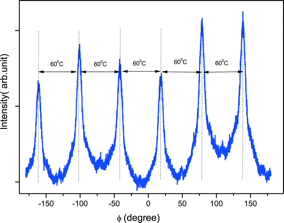 | ||
| Fig. 5 High resolution Φ scan of ZnO films after 72 hour growth in the continuous circulation reactor. | ||
Analyses of optical properties of ZnO films are important for the potential applications in ZnO based optoelectronic devices. Fig. 6 presents the room temperature PL spectra of ZnO films with and without the moderate thermal treatment at 300 °C in air ambient for 30 minutes. It was observed that both near band edge (NBE) and deep level emissions (DLE) increased after heat treatment, the increase in NBE being more significant as borne out by the increase in the NBE to DLE ratio from 0.4 to 3.84 after heat treatment. The NBE to DLE ratio after heat treatment at 300 °C can be comparable to some ZnO films grown at 600 °C by RF magnetron sputtering28 and even better than that for ZnO films grown between 500 and 800 °C by pulsed laser deposition.29
 | ||
| Fig. 6 Room temperature photoluminescence spectra of ZnO films with and without heat treatment: as-grown (AG), heat treated (HT), Gaussian fitting (AG), Gaussian fitting (HT). | ||
The increase in both NBE and DLE intensities suggests an increase in carrier concentration. It is known that H acts as a shallow donor in solution synthesized ZnO30 that is responsible for the intrinsic n-type conductivity and that low temperature heat treatments (200 and 300 °C) can lead to significant increases in carrier concentration, with the heat treatment presumably acting to activate the donors.31 Sim et al.32 have also shown that the increase in carrier concentration can be linked to a surface effect. It was explained that since solution synthesized ZnO films have positively charged zinc terminated surfaces, an electric field is generated which causes holes to sweep away from and electrons to move towards the surface, creating a depletion region in which the probability of electron–hole pairs recombining is lowered. Upon annealing in an oxygen environment, oxygen atoms attaching to the surface reduce the net positive charge of the surface, leading to a reduction in the width of the depletion region and an accompanying increase in radiative recombination.
Multiple Gaussian peak fitting showed that the DLE for the as-grown film was made up of green and orange-red bands at 550 nm (2.25 eV) and 640 nm (1.94 eV) that involved deeply trapped charged carriers.33 After the thermal treatment at 300 °C in air, the orange-red band became more prominent. The origins of these DLE bands are still being debated in the literature, with reports in the literature assigning the green band to either oxygen vacancies or zinc interstitials.30,34,35
On the other hand, an earlier study on solution synthesized ZnO30 assigned green emission to zinc vacancies while interstitial oxygen was responsible for the orange-red band. The presence of zinc vacancies in solution synthesized ZnO has been confirmed by absorption spectroscopy and total scattering experiments.36
Hall measurements showed that the ZnO film had a carrier concentration of 3.12 × 1018 cm−3 with a mobility of 9.75 cm2 V−1 s−1 after heat treatment at 300 °C in air, which are significant increases from its as-grown values of 9.0 × 1017 cm−3 and 0.256 cm2 V−1 s−1. The increase in carrier concentration is consistent with the earlier explanation for increases in PL intensities. Usually, when the carrier concentration increases, the mobility could be expected to decrease due to the increased probability of carrier collisions. That the mobility actually increased by more than one order of magnitude indicates the elimination of defects that could act as recombination centers, including defects responsible for non-radiative recombination. This could also explain the more significant improvement in the NBE after heat treatment.
The carrier concentration and mobility of the heat treated ZnO film grown in this study compare quite well with those of ZnO films grown by nanorod LEO by MOCVD which reported a carrier concentration of 3.4 × 1018 cm−3 and a mobility of 20 cm2 V−1 s−1,8 although the MOCVD grown films had a much rougher surface and had a higher processing temperature of 420 °C.
The crystalline property of the films will be affected by the defect density in the film, including surface defects/interface state, point defects (Zn vacancies, O interstitials), and line defects (dislocations). These types of defect centers need to be reduced to improve the film's crystallinity. According to Ko et al.,37 threading dislocations are often considered to be the main non-radiative recombination centers. Andeen et al.6 and Zhang et al.26 demonstrated that lateral epitaxially overgrown ZnO films have much lower threading dislocation densities (~108 cm−2) and the first report in particular observed a much stronger band edge's PL intensity from regions having a much lower threading dislocation density. Therefore, our main goal in this study is to reduce the threading dislocation's density but without the need for lithography or patterning.
Fig. 7a shows a cross sectional TEM image of ZnO film grown using the continuous circulation reactor for 72 hours after 30 s etching. It shows that the V shaped pits can be associated with threading dislocations. The inset also shows the corresponding selected area diffraction pattern of the film which confirmed the single crystalline nature of the film. From SEM of the film surface morphology after etching (Fig. 7b), these V-pits have a hexagonal symmetry and most pits can be found at the boundaries of the coalesced islands. The average threading dislocation density was estimated to be around 7.8 × 108 cm−2 through the determination of the V-pit density.
 | ||
| Fig. 7 (a) Cross sectional TEM images of ZnO film with 72 hour growth after surface etching (inset) selected area diffraction pattern of the film. (b) Top view FE-SEM image of ZnO film after surface etching for 30 s. | ||
Dependence of dislocation density on the growth time (i.e. film thickness) is shown in Fig. 8. With longer growth time, the threading dislocation's density was significantly reduced with a value of 5 × 108 cm−2 after 168 hours of growth. This is not surprising since it is believed that grain growth of the epitaxially oriented columnar grains will reduce the number of grain boundaries along which most of the threading dislocations are found.30 In addition, this value is comparable with that of solution grown films using the LEO method that utilized lithography fabricated photo-resist masks to reduce the threading dislocations and much lower than the threading dislocation density of normal solution grown ZnO films (~2 × 1010 cm−2).6 This demonstrates that the nanorod LEO method coupled with a continuous circulation reactor is a promising method for producing solution grown ZnO films on the cheaper and larger sapphire substrates, compared to spinel substrates.
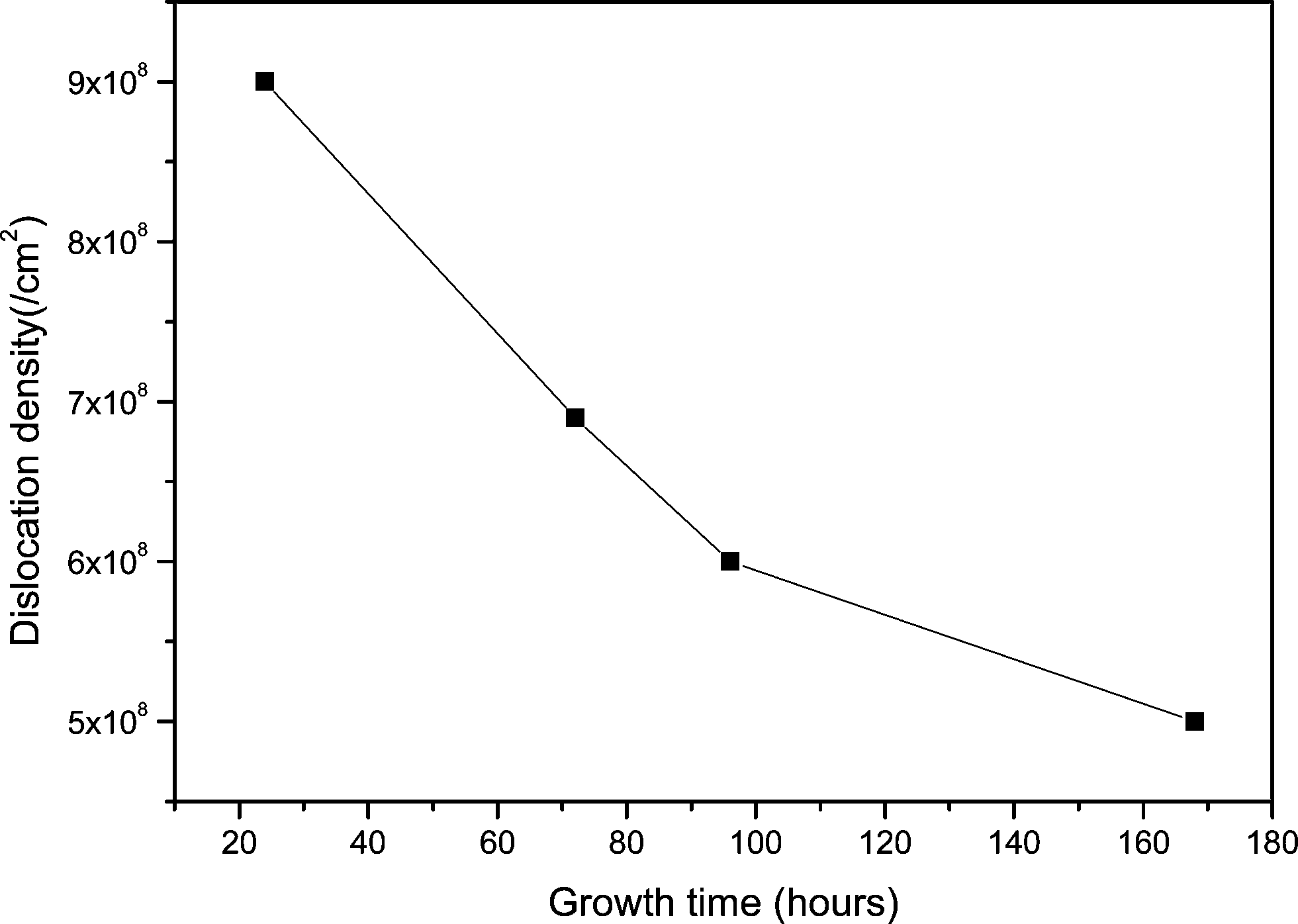 | ||
| Fig. 8 Dependence of threading dislocation density with growth time. | ||
4. Conclusion
A novel method was developed to grow epitaxial ZnO films on c-plane sapphire substrates by employing a nanorod assisted lateral epitaxial overgrowth process at a low growth temperature of 90 °C in water utilizing a continuous circulation reactor. The films were relatively smooth after coalescing by lateral overgrowth of nanorods grown on the spinel buffer layer, without the need for any masks and/or photolithography. The continuous circulation reactor utilized the retrograde solubility of ZnO in water with ammonia additions to provide a constant supersaturated growth solution and the closed loop design enabled the growth of thick films without any waste by-products or the need to refresh the precursor solution.The epitaxial relationship between the grown ZnO film and the sapphire substrate was confirmed by off-axis φ scans and by TEM selected area electron diffraction patterns. Films grown after 72 hours showed good optical properties and a high carrier concentration of 3.12 × 1018 cm−3 and mobility of 9.75 cm2 V−1 s−1 after thermal treatment at 300 °C. The threading dislocation density of the nanorod assisted LEO film was 2 orders of magnitude lower than that of normal solution grown ZnO films, with the lowest value of 5 × 108 cm−2 for the longest growth period.
Acknowledgements
The authors would like to thank Dr. Jacob J. Richardson, University of California Santa Barbara, for valuable technical assistance and Mr. Lim Poh Chong, Institute of Materials Research and Engineering, for assistance in XRD characterization. The authors also acknowledge funding support from the A*STAR-MND Green Building joint grant no. 1121760022.References
- F. Qian, S. Gradecak, Y. Li, C. Y. Wen and C. M. Lieber, Nano Lett., 2005, 5, 2287 CrossRef CAS PubMed.
- Y. Cui, Z. Zhong, D. Wang, W. U. Wang and C. M. Lieber, Nano Lett., 2003, 3, 149 CrossRef CAS.
- J. H. Lim, C. K. Kang, K. K. Kim, I. K. Park, D. K. Hwang and S. J. Park, Adv. Mater., 2006, 18, 2720 CrossRef CAS.
- S. H. K. Park, C. S. Hwang, M. Pyu, S. Yang, C. Byun, J. Shin, J. I. Lee, K. Lee and M. S. Oh, Adv. Mater., 2009, 21, 678 CrossRef CAS.
- B. A. Haskell, F. Wu, M. D. Craven, S. Matsuda, P. T. Fini, T. Fujii, K. Fujito and S. Nakamura, Appl. Phys. Lett., 2003, 83, 644 CrossRef CAS.
- D. Andeen, J. H. Kim, F. F. Lange, G. K. L. Goh and T. Sudhiranjan, Adv. Funct. Mater., 2006, 16, 799 CrossRef CAS.
- G. K. L. Goh, US Provisional Application No. 61/351,066, 3 June 2010 Search PubMed.
- D. C. Kim, J. H. Lee, H. K. Cho, J. H. Kim and J. Y. Lee, Cryst. Growth Des., 2010, 10, 321 CAS.
- Z. K. Tang, G. K. L. Wong, P. Yu, M. Kawasaki, A. Ohtomo, H. Koinuma and Y. Segawa, Appl. Phys. Lett., 1998, 72, 3270 CrossRef CAS.
- Y. Chen, D. Bagnall and T. Yao, Mater. Sci. Eng., B, 2001, 75, 190 CrossRef.
- J. Ye, S. Gu, S. Zhu, T. Chen, L. Hu, F. Qin, R. Zhang, Y. Shi and Y. Zheng, J. Cryst. Growth, 2002, 243, 151 CrossRef CAS.
- P. M. Verghese and D. R. Clarke, J. Mater. Res., 1999, 14, 1039 CrossRef CAS.
- H. Saeki, H. Tabata and T. Kawai, Solid State Commun., 2001, 120, 439 CrossRef CAS.
- B. Wang, E. Shi, W. Zhong and Z. Yin, Chin. Sci. Bull., 1997, 42, 1041 CrossRef CAS.
- D. Andeen, L. Loeffler, N. Padture and F. F. Lange, J. Cryst. Growth, 2003, 259, 103 CrossRef CAS.
- S. K. Lim, H. Q. Le, G. K. L. Goh, K. K. Lin and S. B. Dolmanan, Mater. Res. Innovations, 2011, 15, 401 CrossRef CAS PubMed.
- H. Q. Le, S. K. Lim, G. K. L. Goh, S. J. Chua, N. S. S. Ang and W. Liu, Appl. Phys. B: Lasers Opt., 2010, 100, 705 CrossRef CAS.
- L. N. Demianets, D. V. Kostomarov, I. P. Kuz'mina and S. V. Pushko, Crystallogr. Rep., 2002, 47, S86 CrossRef CAS.
- R. A. Laudise and A. A. Ballman, J. Phys. Chem., 1960, 64(5), 688 CrossRef CAS.
- D. Ehrentraut, H. Sato, Y. Kagamitani, A. Yoshikawa and T. Fukuda, Prog. Cryst. Growth Charact. Mater., 2006, 52, 280 CrossRef CAS PubMed.
- F. F. Lange, Science, 1996, 273, 903 CAS.
- J. J. Richarson and F. F. Lange, Cryst. Growth Des., 2009, 9(6), 2570 Search PubMed.
- J. J. Richarson and F. F. Lange, Cryst. Growth Des., 2009, 9(6), 2576 Search PubMed.
- G. P. Li, L. Jiang, S. J. Wang, X. W. Sun, X. Chen and T. Wu, Cryst. Growth Des., 2011, 11, 4885 CAS.
- L. E. Greene, M. Law, J. Goldberger, F. Kim, J. C. Johnson, Y. F. Zhang, R. J. Saykally and P. D. Yang, Angew. Chem., Int. Ed., 2003, 42, 3031 CrossRef CAS PubMed.
- Y. B. Zhang, G. K. L. Goh and S. Li, Thin Solid Films, 2010, 518, e104 CrossRef PubMed.
- L. L. Liew, H. Q. Le and G. K. L. Goh, Mater. Res. Innovations, 2011, 15, 357 CrossRef CAS PubMed.
- K.-K. Kim, J.-H. Song, H.-J. Jung, W.-K. Choi, S.-J. Park, J.-H. Song and J.-Y. Lee, J. Vac. Sci. Technol., A, 2000, 18, 2864 CAS.
- X. W. Sun and H. S. Kwok, J. Appl. Phys., 1999, 86, 408 CrossRef CAS.
- Y. B. Zhang, G. K. L. Goh, K. F. Ooi and S. Tripathy, J. Appl. Phys., 2010, 108, 083716 CrossRef.
- J. J. Richardson, G. K. L. Goh, H. Q. Le, L. L. Liew, F. F. Lange and S. P. DenBaars, Cryst. Growth Des., 2011, 11, 3558 CAS.
- A. Y. L. Sim, G. K. L. Goh, S. Tripathy, D. Andeen and F. F. Lange, Electrochim. Acta, 2007, 52, 2933 CrossRef CAS PubMed.
- A. Van Dijken, E. A. Meulenkamp, D. Vanmaekelbergh and A. Meijerink, J. Lumin., 2000, 90, 123 CrossRef CAS.
- P. Kumar, L. S. Panchakarla, S. V. Bhat, U. Maitra, K. S. Subrahmanyam and C. N. R. Rao, Nanotechnology, 2010, 21, 385701 CrossRef PubMed.
- B. Das, P. Kumar and C. N. R. Rao, J. Cluster Sci., 2012, 23, 649 CrossRef CAS PubMed.
- Y. L.-L. Liew, G. Sankar, A. D. Handoko, G. K. L. Goh and S. Kohara, J. Solid State Chem., 2012, 189, 63 CrossRef PubMed.
- H. J. Ko, T. Yao, Y. F. Chen and S. K. Hong, J. Appl. Phys., 2002, 92, 4354 CrossRef CAS.
| This journal is © The Royal Society of Chemistry 2014 |