DOI:
10.1039/C3CE41342J
(Paper)
CrystEngComm, 2014,
16, 56-63
Crystal structure tailoring of Au–Cu alloy NPs using the embedding film matrix as template†
Received
9th July 2013
, Accepted 24th August 2013
First published on 29th August 2013
Introduction
Noble metal nanoparticles (NPs) especially the bimetallic NPs have been studied extensively because several important applications are associated with them.1–12 Formation of bimetallic NPs causes plasmonic hybridization, and as a result their plasmonic absorptions can be tuned.13–22 Among the various bimetallic compositions, Au–Cu alloy NPs show remarkable catalytic properties in a wide range of oxidation reactions, and especially in the CO oxidation reaction at low temperature.23–32 A very recent report reveals that the Au–Cu alloy NPs can show tunable photo luminescent emissions in the NIR region.33
Bulk Au–Cu alloy crystal mainly exhibits two stable phases, face centered tetragonal (fct, ordered), and face centered cubic (fcc, disordered).34–37 Au–Cu ordered structure (fct) has alternating stacking of Au and Cu layers along the c-axis; the separation of Au and Cu in layers makes distortion and as a result, tetragonal structure has been formed (Fig. 1a). In disordered structure Au and Cu atoms are arranged in the face centered cubic lattice in an interlocking manner (Fig. 1b).38 Formation of ordered tetragonal Au–Cu alloy formation is generally observed during sequentially implanted in SiO239,40 and disordered fcc structure is found to be observed in cases of sol–gel derived Au/Cu co-doped SiO2 films at relatively high temperature (~800 °C).41–43 Many researchers have shown the order–disorder phase transition of the Au–Cu alloy using temperature dependent studies and the probable mechanism was suggested.34–37,44,45 In the present study, we report for the first time a controlled synthesis of ordered and disordered Au–Cu nanocrystals using isostructural dielectric crystalline film matrix as templates. The crystalline phase formation of Au–Cu nanocrystals has been directed by the host film matrix.
 |
| | Fig. 1 (a) Ordered (fct) and (b) disordered (fcc) structure of Au–Cu alloy. | |
This work thus describes the templated synthesis of fct and fcc Au–Cu alloy NPs in TiO2, ZrO2 and SiO2 film matrices at relatively low temperature and their structural characterization and optical properties. Using various techniques such as UV-visible spectroscopy, transmission electron microscopy (TEM) and grazing incidence X-ray diffraction (GIXRD), we have characterized their physical properties in a comprehensive way. The ordered fct Au–Cu alloy has been generated inside the anatase TiO2 matrix at 500 °C. Anatase TiO2, which has itself a tetragonal structure, assists the formation of ordered tetragonal Au–Cu alloy. Similarly, cubic structure of ZrO2 film host induces the formation of fcc Au–Cu alloy NPs. For comparative study the structure of Au–Cu alloy inside the amorphous SiO matrix has also been investigated. However, without any influence of embedding matrix partial Au–Cu (Au3Cu1) alloy is found to be formed in SiO2 at 500 °C.
Experimental
Materials
All chemicals were used as received. Tetraethyl orthosilicate (TEOS), titanium(IV) isopropoxide (TIP) (97%), zirconium(IV) propoxide (ZP) (70% in n-propanol) and CuCl2∙2H2O were supplied by Sigma-Aldrich while HAuCl4∙3H2O was purchased from S. D. Fine-Chem Limited, India (LR grade). Acetylacetone (acac), hydrochloric acid and n-butanol were purchased from Ranbaxy Fine Chemicals. Millipore water (specific resistance: 18.2 MΩ cm) was used. Compressed gas mixture 10% hydrogen balance argon was obtained from BOC India Ltd.
Preparation of TiO2 and ZrO2 sols
For the preparation of TiO2 and ZrO2 sols the required amount of respective metal alkoxide (TIP or ZP) was first dissolved in n-butanol (60% of the total) and stirred for 30 min. To this alkoxide solution calculated amount of acetylacetone (acac; 0.33 mol per mol of alkoxide) was added with stirring. Water (2 mol per mol of alkoxide) acidified with HCl (2 × 10⁻⁴ mol per mol of alkoxide) mixed with n-butanol (remaining 40%) was then added slowly while stirring and the stirring was continued for about 2 h to complete the hydrolysis and condensation reactions. The clear sols thus obtained were used for metal ion doping.
Preparation of SiO2 sol
The required amount of TEOS was dissolved in n-butanol (60% of the total) and stirred for 30 min to obtained homogeneous solution. To this solution H2O (2 mol per mol of alkoxide) acidified with HCl (2 × 10⁻⁴ mol per mol of alkoxide) and remaining 40% n-butanol mixture was added with stirring. The resulting solution was then refluxed under normal atmospheric pressure for 60 min to complete the hydrolysis and condensation reactions. The clear solution was used for metal ion doping.
Metal ion doping
The molar ratio of metal (Au and Cu) to the TiO2, ZrO2 and SiO2 was kept constant in all the cases being 10 equivalent mol% metal (5 mol% Au and Cu each; Au![[thin space (1/6-em)]](https://www.rsc.org/images/entities/char_2009.gif) :Cu = 5:5) and balance oxide. For metal ion doping the calculated amount of metal salts (HAuCl4∙3H2O and CuCl2∙2H2O) were dissolved in minimum amount of water and mixed with the sols. In case of TiO2 and ZrO2 sols after the addition of Au and Cu the sols became slightly cloudy. However, after addition of 2–3 drops of HCl–n-propanol mixture (1:1 by volume) the sols became transparent, and they were ready for coating depositions. About 8 equivalent wt% of TiO2, ZrO2 and SiO2 was maintained in all the final coating sols.
:Cu = 5:5) and balance oxide. For metal ion doping the calculated amount of metal salts (HAuCl4∙3H2O and CuCl2∙2H2O) were dissolved in minimum amount of water and mixed with the sols. In case of TiO2 and ZrO2 sols after the addition of Au and Cu the sols became slightly cloudy. However, after addition of 2–3 drops of HCl–n-propanol mixture (1:1 by volume) the sols became transparent, and they were ready for coating depositions. About 8 equivalent wt% of TiO2, ZrO2 and SiO2 was maintained in all the final coating sols.
Preparation of films
Prior to the coating deposition, the silica glass slides (Heraus, Suprasil 3; thickness 0.5 mm) were first cleaned with a warm neutral detergent solution, followed by rinsing with distilled water and i-propanol, and finally, boiled in i-propanol for 5 min. The coatings were prepared by the dipping technique (Dip-master 200, Chemat Corporation) with a withdrawal velocity of 6 in min−1. The coated films were dried at 60 °C for 1 h and followed by heat-treated at 500 °C (ramp 2 deg min−1) in air for 1 h to remove the organics. The films were then annealed at 500 °C in 10%H2–90%Ar (H2–Ar) atmosphere with a holding time of 1 h to complete the alloy formation. The preparation of sols and films are shown schematically in Fig. 2.
 |
| | Fig. 2 Schematic representation for the preparation of the Au/Cu incorporated MO2 sols and films (M = Ti, Zr and Si). RT represents room temperature. | |
Characterization of the films
UV-visible spectra of coatings deposited on glass substrates were obtained using a Cary 50 Scan spectrophotometer. Grazing incidence X-ray diffraction (GIXRD) patterns of the films were recorded on Rigaku Smart lab diffractometer operating at 9 kW (200 mA × 45 kV) with Cu-Kα radiation (λ = 1.5405 Å). A 0.3° grazing incidence angle was maintained for all the measurements. Transmission electron microscopic (TEM) measurements were carried out using Tecnai G2 30ST (FEI) operating at 300 kV attached with an energy dispersive X-ray scattering (EDS) unit. The TEM samples were prepared using scratched off films dispersed in methanol. A small drop of this dispersion was placed on a carbon coated Mo grid underlying a tissue paper, dried at 60 °C and analyzed by TEM. The thickness of the Au-Cu doped films were measured ellipsometrically by fitting the refractive index (n), extinction coefficient (k) curves in the non-absorbing region (800–1000 nm).46
Results and discussion
Au/Cu codoped sols were light greenish yellow in colour due to the presence of AuCl4− and Cu2+ ions. The films prepared from the sols were first dried at 60 °C for 1 h and followed by heat-treated at 500 °C in air to remove the organics and annealed further in reducing atmosphere (H2–Ar) at 500 °C. All the heat-treated films were visually clear, transparent and crack free. The film thickness values of the final heat-treated films were measured by spectroscopic ellipsometry. The thickness of annealed Au/Cu doped TiO2, ZrO2 and SiO2 films were found to be 124 ± 3, 109 ± 3 and 185 ± 5 nm, respectively. The corresponding matrix refractive index values were 2.17 (TiO2), 1.93 (ZrO2) and 1.46 (SiO2).
Optical absorption
Fig. 3 shows the UV-visible absorption spectra of Au/Cu incorporated films heat-treated in air and H2–Ar atmospheres, and the corresponding photographs of the films are shown in Fig. S1 (ESI†) Au/Cu doped TiO2 and ZrO2 films heat-treated at 500 °C in air show blue in colour (Fig. S1; ESI†) due to the surface plasmon (SP) absorption of Au nanoparticles (NPs) at 596 and 607 nm for TiO2 and ZrO2 films, respectively. The corresponding Au/Cu doped SiO2 film shows pink colour (Fig. S1; ESI†) due to the SP absorption of Au NPs at 550 nm. The position of Au SP absorptions is found to be different in these films. This is because the plasmonic absorption is related to the dielectric environment (refractive index) of the embedding film matrices. Since the refractive index of TiO2 and ZrO2 films are higher than SiO2, the Au SP absorptions are red-shifted in former cases.47 Up to this stage Cu remains in ionic form (possibly CuO) in all the films because heat-treatment was done in air (oxidising atmosphere). However, no noticeable optical absorption due to Cu2+ was observed because of very weak d–d transition compare to that of strong plasmonic absorption of Au NPs. So the optical absorptions confirm the formation of metallic Au NPs after heat-treatment in air whereas Cu remains in ionic form at this stage. To obtain a solid solution of Au and Cu, films were heat-treated in reducing atmosphere (500 °C/H2–Ar). During the heat-treatment in H2–Ar at 500 °C, Cu ions starts reducing and form Au–Cu solid solution in a simultaneous manner. It was found from our previous studies that the peak positions in the absorption spectra of the Au–Cu alloy were located in between those of the pure Au and Cu.41–43 Here also after heat treatment in the reducing atmosphere all the absorption spectra shifted towards higher wavelength indicating alloy formation. Slight colour changes of the films in accordance with the absorption spectra were also noticed after the formation of Au–Cu alloy (see the photographs of the films; Fig. S1; ESI†).
 |
| | Fig. 3 UV-visible spectra of Au/Cu incorporated (a) TiO2 (b) ZrO2 and (c) SiO2 films annealed at 500 °C in air and H2–Ar. | |
GIXRD studies
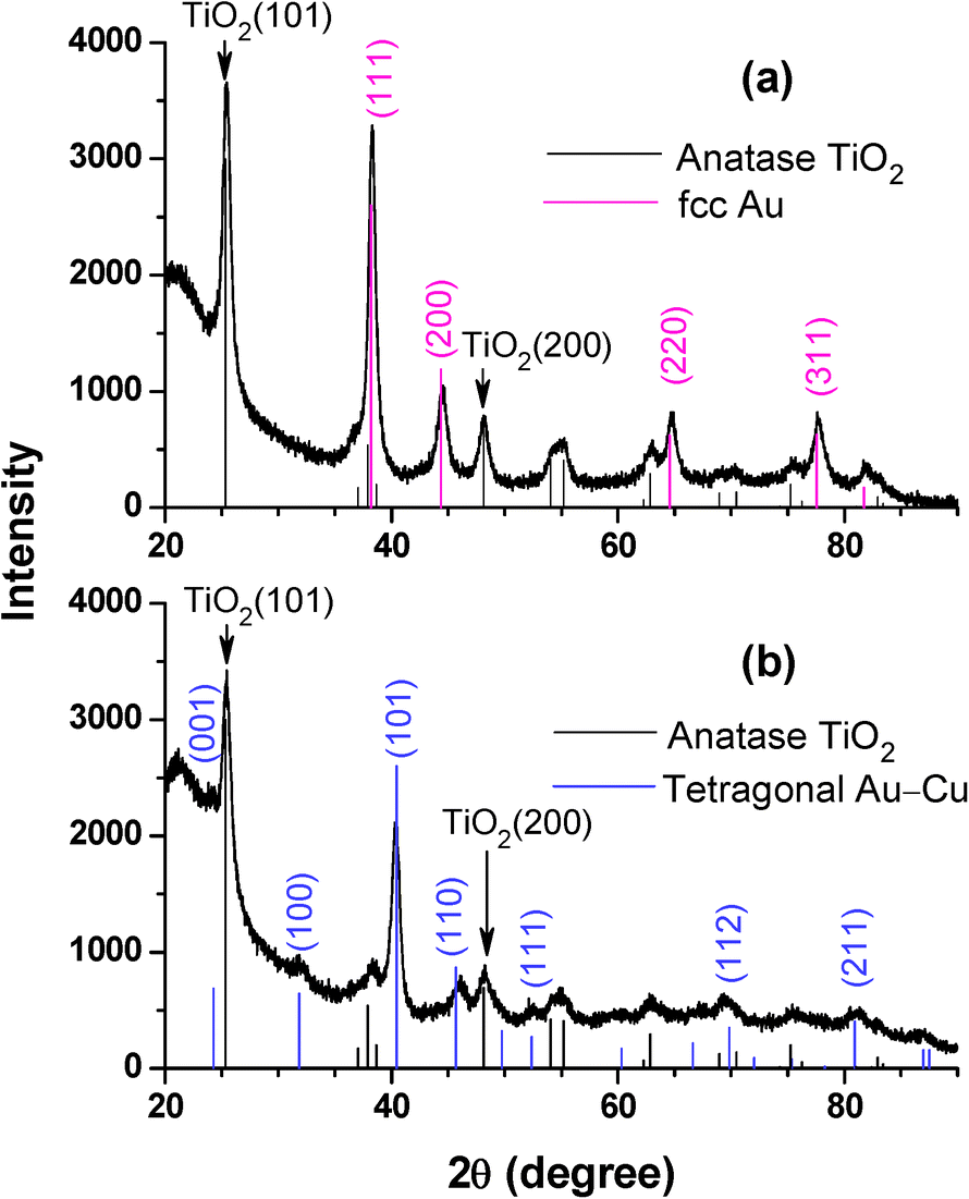
GIXRD studies of the Au/Cu doped SiO2, TiO2 and ZrO2 films were carried out for the evolution of alloy composition and the structure of the alloy. GIXRD of Au/Cu doped TiO2 film heat-treated at 500 °C in oxidising (air) and reducing (H2–Ar) atmospheres are presented in Fig. 4. Heat-treatment in air at 500 °C (Fig. 4a) causes crystallization of TiO2 into anatase structure (tetragonal) along with the formation of Au NPs inside the anatase TiO2 film. As a result, diffraction peaks due to fcc Au (PDF file # 00-04-0784) and anatase TiO2 (PDF file # 01-075-2552) were observed. Cu originated diffraction peaks were not observed (Fig. 4a). The strong diffraction peak observed at 2θ = 25.23° (d = 0.352 nm) corresponds to the (101) lattice plane of anatase TiO2 and the intense peak at 2θ = 38.18° (d = 0.235 nm) is due to the (111) lattice plane of fcc Au. In this atmosphere a solid solution between Au and Cu could not be formed because Cu cannot be reduced in oxidising (air) atmosphere. Upon heat-treatment at 500 °C in reducing atmosphere (H2–Ar) Cu ions were reduced and formed alloy between Au and Cu. As a result of alloy formation, the Au–Cu alloy originated diffraction peaks along with the peaks corresponding to the anatase TiO2 were observed in the XRD (Fig. 4b). The calculated lattice spacing (d) from the (101) peak of Au–Cu is 0.223 nm. The XRD data confirms the formation of ordered tetragonal Au–Cu alloy (commonly known as tetra-auricupride) inside anatase TiO2 matrix. At 500 °C in air matrix TiO2 crystallizes to anatase which itself has tetragonal structure. The tetragonal crystal structure of TiO2 acted as a template and facilitated the formation of ordered tetragonal Au1Cu1 alloy (PDF file # 01-089-2037) only. It is noteworthy here that in previous studies the Au–Cu alloy formation of nearly 1:1 composition was found to occurr at about 700–800 °C.41,42 Here the complete alloy formation occurred at much lower temperature (500 °C). So the embedding tetragonal structure of TiO2 plays an important role in the formation of tetragonal Au–Cu alloy at such a low temperature.
 |
| | Fig. 4 GIXRD patterns of Au/Cu incorporated TiO2 films annealed at 500 °C in air (a) and H2–Ar (b). The vertical lines with relative intensities are the positions of anatase TiO2, fcc Au and fct Au–Cu. | |
In case of Au/Cu doped ZrO2 film, cubic ZrO2 (PDF file # 01-073-9894) (d111 = 0.292 nm) along with fcc Au (d111 = 0.235 nm) were formed after the heat-treatment at 500 °C in air (Fig. 5a). In this case also no Cu related diffraction peak was observed after air annealing. Further heat treatment at 500 °C in reducing atmosphere (H2–Ar), Cu ions were reduced and formed Au–Cu alloy NPs simultaneously. As shown in the GIXRD pattern (Fig. 5b), clear reflections of cubic ZrO2 and fcc Au–Cu (d111 = 0.224 nm) NPs are observed. In our previous studies on Au–Cu alloy formation in SiO2 film we observed very systematic shifting of the lattice parameter, a of Au–Cu alloy towards higher 2θ (smaller ‘a’) with increasing concentration of Cu.41–43 In this case also the diffraction peak due to Au has been shifted towards higher 2θ value and appeared in between the position of fcc Au and Cu confirming the formation of Au–Cu alloy NPs in cubic ZrO2 film matrix. The alloy composition was calculated using the Vegard's law41–43 and found to be Au51Cu49. Here ZrO2 film matrix acted as a template which itself has a cubic structure and therefore facilitated the formation of Au–Cu fcc alloy at low temperature (500 °C).
 |
| | Fig. 5 GIXRD patterns of Au/Cu incorporated ZrO2 films annealed at 500 °C in air (a) and H2–Ar (b). The vertical lines with relative intensities are the positions of cubic ZrO2, fcc Au and fcc Au–Cu. | |
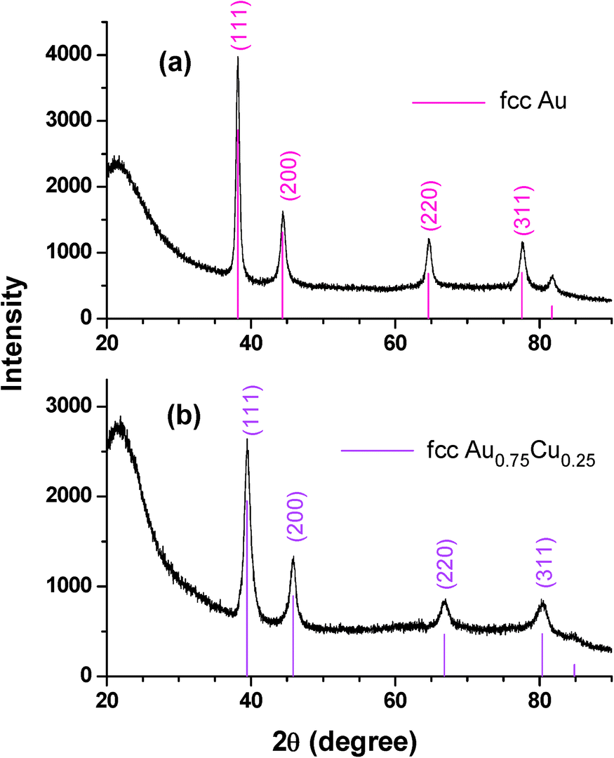
In case of Au/Cu doped SiO2, the matrix remained amorphous after the heat-treatment at 500 °C in air, and the generated fcc Au NPs showed its signature in the XRD (Fig. 6a). In reducing atmosphere (Fig. 6b) fcc Au–Cu alloy NPs (d111 = 0.228 nm) were formed with a compositional ratio of Au75Cu25 (calculated from the shifting of XRD peaks using Vegard's law). As fcc solid solution is more favourable and the embedding matrix has no influence in guiding the structure, the fcc structure of the alloy has been formed as also noticed in our previous studies.41–43 It may be noticed here that as the embedding matrix has no influence, complete alloy formation could not occur at low temperature (500 °C). However, annealing at higher temperature (~800 °C), close to stoichiometric Au–Cu alloy can be formed in SiO2 film matrix.41,42
 |
| | Fig. 6 GIXRD patterns of Au/Cu incorporated SiO2 films annealed at 500 °C in air (a) and H2–Ar (b). The vertical lines with relative intensities are the positions of fcc Au and fcc Au0.75Cu0.25. Matrix SiO2 film remains amorphous in this case. | |
TEM studies
TEM studies of the Au/Cu incorporated TiO2, ZrO2 and SiO2 films heat-treated in both atmospheres of air and H2–Ar at 500 °C were performed for the evaluation of structure, distribution of NPs and composition. Fig. S2 (ESI†) represents the TEM results of Au/Cu incorporated TiO2 films heat-treated at 500 °C in air. The low resolution bright field image (Fig. S2a; ESI†) shows the presence of Au NPs inside TiO2 matrix. The inset of Fig. S2a (ESI†) shows the size distribution of the embedded Au NPs and the calculated average size was found to be 15 nm. The EDS spectrum obtained from the area seen in Fig. S1a (ESI†) is given in Fig. S2b (ESI†), which shows the presence of Ti, O, Au and Cu. The peaks of C and Mo were from carbon coated Mo grid used for TEM studies. The atomic ratio of Au and Cu was found to be Au:Cu = 51.4:48.6 which is also very close to the nominal value (1:1 composition ratio). It is noteworthy here that Cu is not visible in TEM because it remains uniformly distributed in the matrix in ionic form. The SAED pattern (Fig. S2c; ESI†), shows diffraction rings corresponding to anatase TiO2 and fcc Au, which is in agreement with our GIXRD results (Fig. 4a). The high resolution TEM image (Fig. S2d; ESI†) shows Au NPs embedded in the crystalline TiO2 matrix. As shown in the Fig. S2d,† the crystalline lattice fringes of TiO2 (d = 0.349 nm) as well as Au NP (d = 0.234 nm) can be clearly indexed which is in agreement with the GIXRD (Fig. 4a). TEM results of Au–Cu NPs embedded in the TiO2 film heat-treated at 500 °C in H2–Ar are shown in Fig. 7. The bright field TEM (Fig. 7a) shows the presence of Au–Cu alloy NPs of average size of 26 nm inside the TiO2 matrix and the inset shows particle size distribution. It can be noted that the average size of the NPs increases from about 15 to 26 nm after alloy formation. This is mainly due to the contribution of Cu in to the already nucleated Au NPs during alloying. The corresponding EDS pattern (Fig. 7b) obtained from the bright field TEM image confirmed the presence of Au, Cu, Ti and O. C and Mo were from C coated Mo grid. Quantitative EDS analysis gave an average Au:Cu atomic ratio of 51.5:48.5 which is very close to the nominal (1:1) composition. The SAED pattern (Fig. 7c) showed the spots due to the fct Au–Cu alloy and anatase TiO2. High resolution TEM image (Fig. 7d) shows one embedded Au–Cu NP inside the crystalline TiO2 matrix. Existence of lattice fringes corresponding to the (101) plane of anatase TiO2 (d = 0.348 nm) and (101) plane of the tetragonal Au–Cu alloy (d = 0.223 nm) were also confirmed from HRTEM image. The TEM results are in agreement with the GIXRD data shown in Fig. 4b.
 |
| | Fig. 7 TEM images of the generated tetragonal Au–Cu alloy NPs inside the anatase TiO2 film matrix after annealing at 500 °C in H2–Ar: (a) bright field TEM image showing the embedded Au–Cu alloy NPs in the TiO2 film matrix, inset shows the size distribution; (b) corresponding EDS and (c) SAED pattern taken from the bright field image; (d) the high resolution TEM image showing the (101) crystalline planes of the anatase TiO2 and fct Au–Cu alloy NPs, inset shows the magnified view of the portion indicated by dashed cyan enclosure. | |
Fig. S3 (ESI†) reveals the TEM results of Au/Cu doped ZrO2 films heat-treated at 500 °C in air. Bright field image (Fig. S3a; ESI†) shows the presence of Au NPs inside the ZrO2 matrix. Here also Cu is not visible as also in the case of TiO2 film heat-treated in air. The inset of Fig. S3a (ESI†) shows the particle size distribution of the embedded Au NPs and the calculated average size was found to be 21 nm. The EDS spectrum is given in Fig. S3b, (ESI†) which shows the presence of Zr, O, Au and Cu. The atomic ratio of Au and Cu was found to be Au:Cu = 51.3:48.7 which is also very close to the nominal value of 1:1. The SAED pattern (Fig. S3c; ESI†) shows diffraction rings/spots corresponding to cubic ZrO2 and fcc Au (diffraction ring due to Au is not prominent in the presence of highly crystalline ZrO2).The HRTEM image (Fig. S3d; ESI†) shows clear lattice fringes at d = 0.291, 0.234 nm corresponding to the characteristic ZrO2 (111) and Au (111), respectively. Bright field TEM image (Fig. 8a) of Au–Cu embedded ZrO2 film heat treated at 500 °C in H2 shows presence of Au–Cu alloy NPs having average size of 29 nm inside the ZrO2 matrix. The inset of Fig. 8a shows the size distribution of alloy NPs. Here also the average size of the NPs increases after the alloy formation. EDS analysis (Fig. 8b) and SAED pattern (Fig. 8c) show the elemental and crystalline features, respectively. From quantitative EDS analysis an average Au/Cu atomic ratio of 51:49 was found. HRTEM image (Fig. 8d) shows the lattice fringes corresponding to the (111) crystalline plane of cubic ZrO2 and (111) plane of fcc Au–Cu alloy. This data is well consistent with the result obtained from GIXRD (Fig. 5b).
 |
| | Fig. 8 TEM images of the generated fcc Au–Cu alloy NPs inside the cubic ZrO2 film matrix after annealing at 500 °C in H2–Ar: (a) bright field TEM image showing the embedded Au–Cu alloy NPs in the ZrO2 film matrix, inset shows the size distribution; (b) corresponding EDS and (c) SAED pattern taken from the bright field TEM image; (d) the high resolution TEM image showing the (111) crystalline planes of the cubic ZrO2 and fcc Au–Cu alloy NPs, inset shows the magnified view of the portion indicated by dashed cyan enclosure. | |
The TEM studies of Au/Cu doped SiO2 film annealed at 500 °C in air was also undertaken and the results are presented in Fig. S4 (ESI†), Fig. S4a (ESI†) represents the bright field TEM image. The inset shows the distribution of Au NPs with an average size of 33 nm. The EDS spectrum (Fig. S4b; ESI†) shows the presence of Si, O, Au and Cu. The atomic ratio of Au and Cu was found to be Au:Cu = 53:47. The SAED pattern (Fig. S4c; ESI†) shows diffraction rings corresponding to only fcc Au. The HRTEM image (Fig. S4d; ESI†) shows a single Au NP in the amorphous SiO2 matrix. Bright field image (Fig. 9a) of the film heat-treated at 500 °C in H2–Ar shows the embedded particle of average size 38 nm inside the amorphous SiO2. In this case also the average size of the NPs increases from 33 to 38 nm after heat treatment in reducing atmosphere. SAED pattern (inset of Fig. 9a) shows the crystalline features due to the existence of Au–Cu alloy. HRTEM image (Fig. 9b) confirms the amorphous nature of SiO2 matrix and shows lattice fringes corresponding to the (111) plane of the fcc Au–Cu alloy. Both SAED and HRTEM confirm the alloy composition as Au75Cu25. This TEM data is also well consistent with the result obtained from GIXRD (Fig. 6b). Corresponding EDS pattern (Fig. 9c) obtained from bright field TEM image showed the presence of Au, Cu, Si and O. Quantitative EDS analysis gave an average Au:Cu atomic ratio of 58:42. The Cu concentration includes the excess Cu ions in the matrix which did not reduce and form alloy.
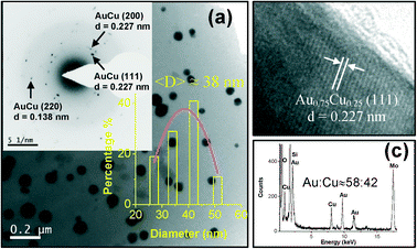 |
| | Fig. 9 TEM images of the generated Au–Cu NPs in SiO2 film annealed at 500 °C in H2–Ar: (a) bright field image showing the embedded Au0.75Cu0.25 alloy NPs in amorphous SiO2 film and inset shows the corresponding SAED pattern and particle size distribution; (b) the high resolution TEM image showing the (111) crystalline plane of the fcc Au0.75Cu0.25 alloy; (c) EDS taken from the bright field TEM image. | |
The above studies showed that fcc Au NPs were first generated in fct TiO2, fcc ZrO2 and amorphous SiO2 film matrices after the heat treatment in air. In the next step during annealing in H2 atmosphere Cu started to reduce and formed solid solution (alloy) with the existing fcc Au NPs, and at this stage the host matrices play a vital role in governing the structure of the Au–Cu alloy. It is noteworthy here that although some structural mismatch in the lattice parameters are found to be present between the fct TiO2 (a = 0.377 nm; c = 0.942 nm) and the generated fct Au–Cu (a = 0.2806 nm; c = 0.3662 nm), the growth of fct Au–Cu occurred smoothly. It is known that anatase TiO2 grows with majority of {101} external surface48 because of its lowest surface energy. Again we can expect a preferential interaction of Cu with the oxygen atoms present on the {101} facets of TiO2.49 So, during the evolution of structure of Au–Cu alloy in TiO2 the most abundant exposed {101} coupled with Cu facilitates the formation of Au–Cu {101} facets i.e. fct structure. In the case of fcc ZrO2 (a = 0.5008 nm) host, metallic Cu (fcc) formed after the reduction immediately dissolved in the fcc Au and formed fcc Au–Cu (a = 0.388 nm; calculated by us using Vegards's law) solid solution. Here the fcc ZrO2 host facilitates the formation of fcc Au–Cu alloy NPs at relatively low temperature.
Conclusions
Ordered and disordered Au–Cu alloy NPs were successfully synthesized in transparent TiO2, ZrO2 and SiO2 film matrices. We observed that the crystal structure of the embedding matrix strongly influences to tailor the structure of the embedded Au–Cu alloy NPs. As a result, tetragonal ordered Au–Cu alloy NPs were formed in tetragonal anatase TiO2 film matrix whereas cubic ZrO2 matrix generated the disordered cubic Au–Cu NPs. In both the cases matrix and embedded NPs were isostructural and the 1:1 (Au1Cu1) NPs were completed at relatively low temperature (500 °C). In amorphous SiO2 under no matrix influence cubic Au–Cu NPs of composition 0.75:0.25 (Au3Cu1) were formed under similar experimental conditions. In this case annealing at higher temperature (~800 °C) in H2–Ar atmosphere is needed for further reduction of the Cu ions in obtaining close to 1:1 alloy NPs. We therefore showed that the embedding matrix can be used as a template to tailor the crystal structure of the embedded NPs at low temperature. Such in situ and transparent dielectric film mediated synthesis of Au–Cu alloy NPs having different crystal structures is noteworthy and the resulting nanocomposite films could be of potential technological interest in optical, photocatalytic and related applications.
Acknowledgments
DST, Govt. of India is thankfully acknowledged for financial support. M. K. M. thanks CSIR, India for fellowship.
References
- E. Katz and I. Willner, Angew. Chem., Int. Ed., 2004, 43, 6042 CrossRef CAS PubMed.
- S. E. Habas, H. Lee, V. Radmilovic, G. A. Somorjai and P. Yang, Nat. Mater., 2007, 6, 692 CrossRef CAS PubMed.
- M. B. Cortie and A. M. McDonagh, Chem. Rev., 2011, 111, 3713 CrossRef CAS PubMed.
- M. Tsuji, K. Ikedo, M. Matsunaga and K. Uto, CrystEngComm, 2012, 14, 3411 RSC.
- M. Tsuji, D. Yamaguchi, M. Matsunaga and K. Ikedo, Cryst. Growth Des., 2011, 11, 1995 CAS.
- K. J. Majo, C. De and S. O. Obare, Plasmonics, 2009, 4, 61 CrossRef.
- H. Zeng and S. H. Sun, Adv. Funct. Mater., 2008, 18, 391 CrossRef CAS.
- C. Wang, C. J. Xu, H. Zeng and S. H. Sun, Adv. Mater., 2009, 21, 3045 CrossRef CAS PubMed.
- K. Tedsree, T. Li, S. Jones, C. W. A. Chan, K. M. K. Yu, P. A. J. Bagot, E. A. Marquis, G. D. W. Smith and S. C. E. Tsang, Nat. Nanotechnol., 2011, 6, 302 CrossRef CAS PubMed.
- F. Besenbacher, I. Chorkendorff, B. S. Clausen, B. Hammer, A. M. Molenbroek, J. K. Norskov and I. Stensgaard, Science, 1998, 279, 1913 CrossRef CAS.
- P. R. Sajanlal and T. Pradeep, Langmuir, 2010, 26, 8901 CrossRef CAS PubMed.
- P. R. Sajanlal and T. Pradeep, Langmuir, 2010, 26, 456 CrossRef CAS PubMed.
- A. M. Dallaire, D. Rioux, A. Rachkov, S. Patskovsky and M. Meunier, J. Phys. Chem. C, 2012, 116, 11370 CAS.
- S. Lal, S. Link and N. J. Halas, Nat. Photonics, 2007, 1, 641 CrossRef CAS.
- A. Moores and F. Goettmann, New J. Chem., 2006, 30, 1121 RSC.
- S. Pal and G. De, Chem. Mater., 2005, 17, 6161 CrossRef CAS.
- C. Wang, S. Peng, R. Chan and S. Sun, Small, 2009, 5, 567 CrossRef CAS PubMed.
- S. Liu, G. Chen, P. N. Prasad and M. T. Swihart, Chem. Mater., 2011, 23, 4098 CrossRef CAS.
- H. C. Chen, S. W. Chou, W. H. Tseng, I. W. P. Chen, C. C. Liu, C. Liu, C. Chen, C. I. Wu and P. T. Chou, Adv. Funct. Mater., 2012, 22, 3975 CrossRef CAS.
- Z. Xu, E. Lai, Y. S. Horn and K. H. Schifferli, Chem. Commun., 2012, 48, 5626 RSC.
- N. L. Motl, E. E. Annan, I.T. Sines, L. Jensen and R. E. Schaak, J. Phys. Chem. C, 2010, 114, 19263 CAS.
- S. Pal, S. Bysakh and G. De, J. Nanosci. Nanotechnol., 2010, 10, 775 CrossRef CAS PubMed.
- X. Liu, A. Wang, X. Wang, C. Y. Mouc and T. Zhang, Chem. Commun., 2008, 3187 RSC.
- C. L. Bracey, P. R. Ellisb and G. J. Hutchings, Chem. Soc. Rev., 2009, 38, 2231 RSC.
- X. Liu, A. Wang, T. Zhang, D. S. Su and C. Y. Mou, Catal. Today, 2011, 160, 103 CrossRef CAS PubMed.
- W. Li, A. Wang, X. Liu and T. Zhang, Appl. Catal., A, 2012, 433–434, 146 CrossRef CAS PubMed.
- C. D. Pina, E. Falletta and M. Rossi, J. Catal., 2008, 260, 384 CrossRef PubMed.
- Y. Sugano, Y. Shiraishi, D. Tsukamoto, S. Ichikawa, S. Tanaka and T. Hirai, Angew. Chem., Int. Ed., 2013, 52, 5295 CrossRef CAS PubMed.
- S. Kameoka and A. P. Tsai, Catal. Lett., 2007, 121, 337 CrossRef.
- X. Li, S. S. S. Fang, J. Teo, Y. L. Foo, A. Borgna, M. Lin and Z. Zhong, ACS Catal., 2012, 2, 360 CrossRef CAS.
- R. J. Chimentao, F. Medina, J. L. G. Fierro, J. Llorca, J. E. Sueiras, Y. Cesteros and P. Salagre, J. Mol. Catal. A: Chem., 2007, 274, 159 CrossRef CAS PubMed.
- J. C. Bauer, D. Mullins, M. Li, Z. Wu, E. A. Payzant, S. H. Overbury and S. Dai, Phys. Chem. Chem. Phys., 2011, 13, 2571 RSC.
- C. M. Andolina, A. C. Dewar, A. M. Smith, L. E. Marbella, M. J. Hartmann and J. E. Millstone, J. Am. Chem. Soc., 2013, 135, 5266 CrossRef CAS PubMed.
- M. Ohta, M. Nakagawa and K. Yasuda, J. Mater. Sci., 1990, 25, 5025 CrossRef CAS.
- Y. Tanaka, K. Udoh, K. Hisatsune and K. Yasuda, Mater. Trans., 1998, 39, 87 CAS.
- L. Battezzati, M. Belotti and V. Brunella, Scr. Mater., 2001, 44, 2759 CrossRef CAS.
- H. Okamoto, D. J. Chakrabarti, D. E. Laughlin and T. B. Massalski, Bull. Alloy Phase Diagrams, 1987, 8, 454 CrossRef CAS.
-
W. Hume-Rothery, Applications of X-ray Diffraction to Metallurgical Science, 1962, Springer, Ch. 12, pp 205–206 Search PubMed.
- F. Gonella, G. Mattei, P. Mazzoldi, C. Sada, G. Battaglin and E. Cattaruzza, Appl. Phys. Lett., 1999, 75, 55 CrossRef CAS.
- C. Maurizio, G. Mattei, P. Mazzoldi, S. Padovani, E. Cattaruzza, F. Gonella, F. D'Acapito and F. Zontone, Nucl. Instrum. Methods Phys. Res., Sect. B, 2000, 200, 178 CrossRef.
- G. De and C. N. R. Rao, J. Phys. Chem. B, 2003, 107, 13597 CrossRef CAS.
- S. Pal and G. De, J. Mater. Chem., 2007, 17, 493 RSC.
- G. De, G. Mattei, P. Mazzoldi, C. Sada, G. Battaglin and A. Quaranta, Chem. Mater., 2000, 12, 2157 CrossRef CAS.
- T. Cleason and J. B. Bouce, Phys. Rev. B, 1984, 29, 1551 CrossRef.
- T. Anraku1, I. Sakaihara, T. Hoshikawa and M. Taniwaki, Mater. Trans., 2009, 50, 683 CrossRef.
- S. Pramanik, S. Pal and G. De, J. Mater. Chem., 2010, 20, 9081 RSC.
- S. K. Medda, S. De and G. De, J. Mater. Chem., 2005, 15, 3278 RSC.
- F. Tian, Y. Zhang, J. Zhang and C. Pan, J. Phys. Chem. C, 2012, 116, 7515 CAS.
- J. A. Rodriguez, J. Evans, J. Graciani, J. B. Park, P. Liu, J. Hrbek and J. F. Sanz, J. Phys. Chem. C, 2009, 113, 7364 CAS.
Footnote |
| † Electronic supplementary information (ESI) available: photographs of the films heat-treated in different atmosphere (Fig. S1), TEM of Au/Cu incorporated MO2 (M = Ti, Zr and Si) films heat-treated in air (Fig. S2–S4). See DOI: 10.1039/c3ce41342j |
|
| This journal is © The Royal Society of Chemistry 2014 |
Click here to see how this site uses Cookies. View our privacy policy here.