
 Open Access Article
 This Open Access Article is licensed under a
 Creative Commons Attribution 3.0 Unported Licence
The aerosol assisted chemical vapour deposition of SnSe and Cu2SnSe3 thin films from molecular precursors†
Punarja
Kevin
a,
Sajid N.
Malik
ab,
Mohammad A.
Malik
a and
Paul
O'Brien
*a
aThe School of Chemistry and The School of Materials, The University of Manchester, Oxford Road, M13 9PL Manchester, UK. E-mail: paul.obrien@manchester.ac.uk; Fax: +44-(0)161-2751411; Tel: +44-(0)161-2751411
bSchool of Chemical and Materials Engineering (SCME), National University of Sciences and Technology (NUST), Islamabad 44000, Pakistan
First published on 29th September 2014
Abstract
Tin selenide (SnSe) and copper tin selenide (Cu2SnSe3) thin films have been deposited onto glass substrates by AACVD using [Sn(Ph2PSe2)2] or a mixture of [Sn(Ph2PSe2)2] and [Cu(acac)2] respectively.
Tin selenide (SnSe) is a p-type semiconductor with a direct band gap of 0.9 eV and an indirect band gap of 1.3 eV. The material finds application in optoelectronic devices,1 as a thermoelectric material and in lithium ion batteries.2 Various methods have been used for the deposition of SnSe thin films which include atmospheric pressure chemical vapour deposition (APCVD),3 pyrolysis,4 thermal evaporation5 and chemical bath deposition (CBD).6 Cu2SnSe3 is also a p-type semiconductor. In both cubic and wurtzitic forms, Cu2SnSe3 has a band gap close to 1.5 eV whereas the rhombohedral form has a direct band gap of 0.84 eV.7 Cu2SnSe3 has a high optical absorption co-efficient >104.8 Its Hole transport is chiefly controlled by the Cu–Se electro-conductive frame work.9 Cu2SnSe3 is based on earth abundant elements, has a simple crystal structure and phase diagram as compared to other quaternary chalcogenides. These features make Cu2SnSe3 an attractive candidate for variety of optoelectronic and solar energy applications.10 The uses of Cu2SnSe3 are being explored in: acousto-optic applications,11 thermo-electronics,12 and biomedical applications.
Cu2SnSe3 nanocrystals have been synthesized by employing a variety of techniques including: a microwave assisted polyol method,13 colloidal synthesis14 and flash evaporation methods.15 However, there are very few reports on the deposition of thin films. Kim et al. have recently reported the growth of Cu2SnSe3 crystals on soda lime glass substrate by the co-evaporation method.16 They studied the effect of substrate temperature on phase transformations between cubic and monoclinic phases and determined optical properties. The precise control of both the morphology and stoichiometry of Cu2SnSe3 films remains a challenge. Chemical Vapour Deposition (CVD) is a promising technique for deposition of such films and can provide control over phase, morphology and microstructure. The utility of conventional CVD is limited by its dependence on volatile precursors. AACVD is a variant of CVD in which less or non-volatile precursors are flash evaporated. Sharma et al. have deposited SnSe thin films by AACVD at 490 °C and 530 °C using a diorganotin(IV)-2-pyridyl selenoate complex as single source precursor.17
Previously, we have reported the synthesis and use of selenophosphinate complexes for deposition of binary, ternary and quaternary metal chalcogenide thin films by AACVD.18,19 Krauss et al. reported the structure and the use of bis(diphenyldiselenophosphinato)lead(II) complex as a precursor for PbSe nanoparticles.20 The deposition of CZTS thin films from diethyldithiocarbamato-complexes of Cu, Zn and Sn by AA-CVD has also been reported.21 Suitable mixtures of precursor materials with comparable thermal decomposition rate facilitate deposition and provide effective stoichiometric control especially in the deposition of more complex semiconductor materials.21 We have now synthesized a new complex bis(diphenylphosphine-diselenoato)tin(II) [Sn(Ph2PSe2)2] and used it as a single source precursor for the deposition of tin selenide (SnSe) thin films by AACVD. We have also used it in combination with bis(2,4-pentanedionato)copper(II) [Cu(acac)2] for the deposition of Cu2SnSe3 thin films.‡
The preparation of [Sn(Ph2PSe2)2] complex was carried out in two steps. Potassium diphenylphosphinodiselenoate was prepared by the reaction of diphenylphosphine, elemental selenium and potassium hydroxide as reported by Gusarova et al.22 The ligand was then reacted with SnCl2 to give corresponding [Sn(Ph2PSe2)2] complex. The product was characterized by FTIR, NMR, mass spectrometry and elemental analysis. Thermogravimetric analysis of the complex showed decomposition between 350 °C and 400 °C to give a ∼21% residue corresponding to SnSe (Fig. S1, ESI†).
The deposition of SnSe by AACVD was carried out by using a 0.19 mmol solution of [Sn(Ph2PSe2)2] in THF (15 mL). Deposition was carried out at 350 and 400 °C with an Ar flow rate of 180 sccm for 45 min. No deposition occurred at 350 °C whereas dark brown, well adhered films were obtained on glass substrates at 400 °C. Fig. 1a shows p-XRD pattern of SnSe thin films deposited at 400 °C. The pattern is indexed to the standard ICDD pattern 00-048-1224 of orthorhombic SnSe with preferred orientation along (111) plane. SEM images (Fig. 1b and c) show the uniform morphology of microcrystalline SnSe thin films. The morphology of the films is based on irregular sheets with an average size of ca. 1.5 μm. Relative atomic percentage of Sn and Se atoms determined by EDX measurements was found to be 48![[thin space (1/6-em)]](https://www.rsc.org/images/entities/char_2009.gif) :52 which is fairly close to the expected value of individual grains. The band gap of SnSe was found to be 1.1 eV (Fig. S2, ESI†) which is close to that reported previously for this material.1
:52 which is fairly close to the expected value of individual grains. The band gap of SnSe was found to be 1.1 eV (Fig. S2, ESI†) which is close to that reported previously for this material.1
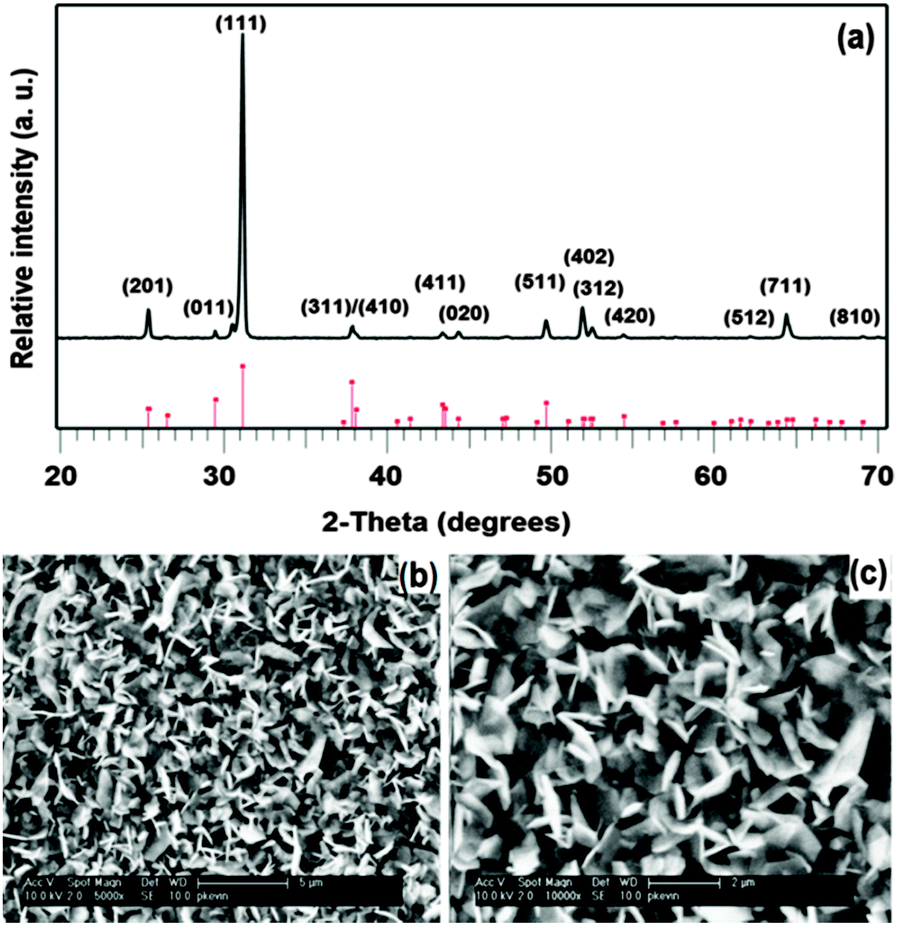 | ||
| Fig. 1 (a) p-XRD pattern of SnSe thin film deposited from [Sn(Ph2PSe2)2] precursor at 400 °C. Vertical lines below show standard ICDD pattern 00-048-1224 for orthorhombic SnSe (b) and (c) SEM images of as deposited thin film at 400 °C. | ||
The deposition of Cu2SnSe3 was carried out by using a mixture of [Cu(acac)2] (0.38 mmol) and [Sn(Ph2PSe2)2] (0.19 mmol) in 15 mL THF at three different temperatures (350, 400 and 450 °C) for 1 hour. Deposition at 350 °C produced no thin films whereas those at 400 and 450 °C produced uniform, shiny dark brown films. The p-XRD patterns (Fig. 2a) of the thin films deposited at 400 °C and 450 °C correspond to the standard ICDD pattern 03-065-4145 for cubic Cu2SnSe3 phase with space group F![[4 with combining macron]](https://www.rsc.org/images/entities/char_0034_0304.gif) 3m.
3m.
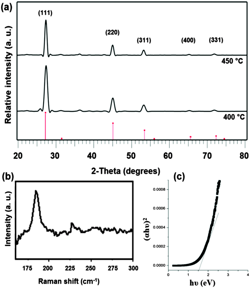 | ||
| Fig. 2 (a) p-XRD pattern of Cu2SnSe3 thin film deposited from [Sn(Ph2PSe2)2] and [Cu(acac)2] precursors at 400 and 450 °C indexed with standard ICDD pattern 03-065-4145 for cubic Cu2SnSe3 (b) Raman spectrum and (c) band gap plot for Cu2SnSe3 thin film deposited at 400 °C. | ||
Films deposited at 400 °C had a uniform morphology (Fig. 3a) whereas two distinct types of crystallites were seen in those deposited at 450 °C. The films deposited at 400 °C consist of clusters of nanocrystalline flakes whilst the images of those deposited at 450 °C show larger semispherical crystallites thinly scattered in a background of irregularly shaped nanocrystallites. EDX analysis showed the chemical composition as Cu:Sn:Se 2.1:1.0:2.9 for thin films deposited at 400 °C and Cu:Sn:Se 1.9:1.0:2.6 for the films deposited at 450 °C. These results clearly show that the films deposited at 400 °C are of better quality being uniform in morphology and having better stoichiometry. The Raman spectrum of the thin films deposited at 400 °C is given in Fig. 2b which shows a strong peak at ∼180.6 cm−1 with a minor peak at 232 cm−1. These peaks correspond with the reported values (179.9 and 231.6 cm−1) for A1 and A2 symmetry modes of Cu2SnSe3.15 The absence of peaks at 150 and 260 cm−1 for CuSe and SnSe shows the deposition of pure Cu2SnSe3. Fig. 2c shows the band gap of the films deposited at 400 °C as ∼1.5 eV. This value is in agreement with that reported previously for Cu2SnSe3.23–25
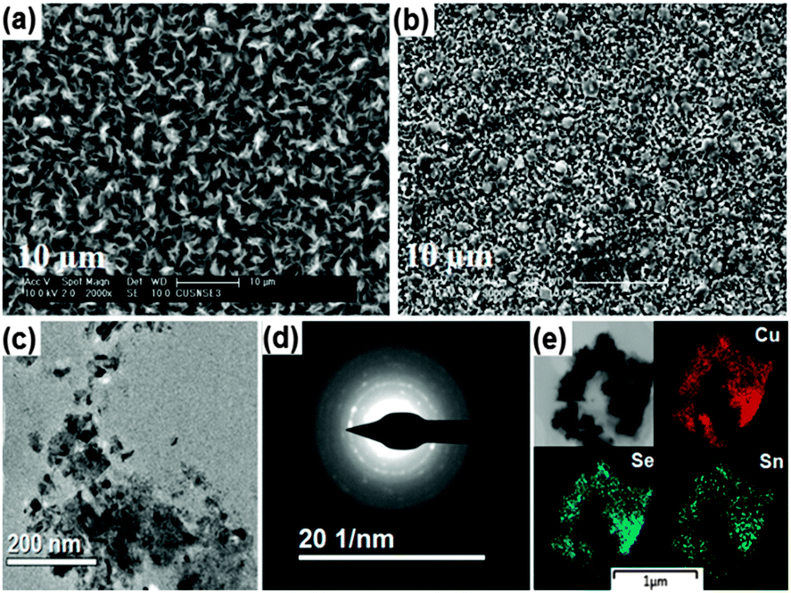 | ||
| Fig. 3 SEM images of Cu2SnSe3 thin films deposited at (a) 400 °C and (b) 450 °C. (c) TEM image (d) SAED pattern and (e) EDX elemental of a single Cu2SnSe3 particle. | ||
The deposited material was scratched from the films deposited at 400 °C and was further investigated by using transmission electron microscopy (TEM). TEM image (Fig. 3c) show similar flake like crystals as observed in SEM. Selected area electron diffraction (SAED) pattern showed distinct rings suggesting the polycrystalline nature of the material (Fig. 3d). Elemental mapping of a single particle as shown in Fig. 3e exhibited even distribution of Cu, Sn and Se in the crystal.
A new complex, [Sn(Ph2PSe2)2] has been synthesised and used as single source precursor in combination with [Cu(acac)2] for the deposition of monophasic tin selenide (SnSe) and copper tin selenide (Cu2SnSe3) thin films onto glass substrates by AACVD at 400 °C and 450 °C. This is the first deposition of thin films of this material by AACVD which has potential applications in photovoltaics and optoelectronics.
We thank EPSRC for funding the instruments under grant number (EP/K039547/1) for characterization of compounds. PK thanks The School of Chemistry, The University of Manchester for funding.
Notes and references
- C. L. Zhang, H. H. Yin, M. Han, Z. H. Dai, H. Pang, Y. L. Zheng, Y. Q. Lan, J. C. Bao and J. M. Zhu, ACS Nano, 2014, 8, 3761–3770 CrossRef CAS PubMed
; P. Kevin, D. J. Lewis, J. Raftery, M. A. Malik and P. O'Brien, J. Cryst. Growth DOI:10.1016/j.jcrysgro.2014.07.019
- E. Schonherr and W. Stetter, J. Cryst. Growth, 1975, 30, 96–98 CrossRef CAS
- N. D. Boscher, C. J. Carmalt, R. G. Palgrave and I. P. Parkin, Thin Solid Films, 2008, 516, 4750–4757 CrossRef CAS PubMed
- P. Boudjouk, D. J. Seidler, S. R. Bahr and G. J. McCarthy, Chem. Mater., 1994, 6, 2108–2112 CrossRef CAS
- C. A. R. M. Sahayaraj, A. Mohan, V. Arivazhagan and S. Rajesh, Chalcogenide Lett., 2014, 11, 47–52 CAS
- B. Pejova and I. Grozdanov, Thin Solid Films, 2007, 515, 5203–5211 CrossRef CAS PubMed
- J. Fan, W. Carrillo-Cabrera, L. Akselrud, I. Antonyshyn, L. D. Chen and Y. Grin, Inorg. Chem., 2013, 52, 11067–11074 CrossRef CAS PubMed
- Y. T. Zhai, S. Y. Chen, J. H. Yang, H. J. Xiang, X. G. Gong, A. Walsh, J. Kang and S. H. Wei, Phys. Rev. B, 2011, 84, 075213 CrossRef
- G. Marcano, C. Rincon, L. M. de Chalbaud, D. B. Bracho and G. S. Perez, J. Appl. Phys., 2001, 90, 1847–1853 CrossRef CAS PubMed
- L. Zhu, Y. H. Qiang, Y. L. Zhao, X. Q. Gu, D. M. Song and C. B. Song, Acta Phys.-Chim. Sin., 2013, 29, 2339–2344 CAS
- G. Marcano, L. M. de Chalbaud, C. Rincon and G. S. Perez, Mater. Lett., 2002, 53, 151–154 CrossRef CAS
- M. Ibanez, D. Cadavid, U. Anselmi-Tamburini, R. Zamani, S. Gorsse, W. H. Li, A. M. Lopez, J. R. Morante, J. Arbiol and A. Cabot, J. Mater. Chem. A, 2013, 1, 1421–1426 CAS
- H. Grisaru, V. G. Pol, A. Gedanken and I. Nowik, Eur. J. Inorg. Chem., 2004, 1859–1864 CrossRef CAS
- J. J. Wang, A. Singh, P. Liu, S. Singh, C. Coughlan, Y. N. Guo and K. M. Ryan, J. Am. Chem. Soc., 2013, 135, 7835–7838 CrossRef CAS PubMed
- G. H. Chandra, O. L. Kumar, R. P. Rao and S. Uthanna, J. Mater. Sci., 2011, 46, 6952–6959 CrossRef
- K. M. Kim, H. Tampo, H. Shibata and S. Niki, Mater. Lett., 2014, 116, 61–63 CrossRef CAS PubMed
- R. K. Sharma, G. Kedarnath, A. Wadawale, C. A. Betty, B. Vishwanadh and V. K. Jain, Dalton Trans., 2012, 41, 12129 RSC
- C. Q. Nguyen, A. Adeogun, M. Afzaal, M. A. Malik and P. O'Brien, Chem. Commun., 2006, 2179 RSC
- S. Mahboob, S. N. Malik, N. Haider, C. Q. Nguyen, M. A. Malik and P. O'Brien, J. Cryst. Growth, 2014, 394, 39–48 CrossRef CAS PubMed
- C. M. Evans, M. E. Evans and T. D. Krauss, J. Am. Chem. Soc., 2010, 132, 10973–10975 CrossRef CAS PubMed
- K. Ramasamy, M. A. Malik and P. O'Brien, Chem. Sci., 2011, 2, 1170 RSC
- A. V. Artem'ev, S. F. Malysheva, N. K. Gusarova and B. A. Trofimov, Synthesis, 2010, 2463–2467 Search PubMed
- J. J. Wang, A. Singh, P. Liu, S. Singh, C. Coughlan, Y. N. Guo and K. M. Ryan, J. Am. Chem. Soc., 2013, 135, 7835–7838 CrossRef CAS PubMed
- S. J. Li and D. C. Pan, J. Cryst. Growth, 2012, 358, 38–42 CrossRef CAS PubMed
- M. E. Norako, M. J. Greaney and R. L. Brutchey, J. Am. Chem. Soc., 2011, 134, 23–26 CrossRef PubMed
Footnotes |
| † Electronic supplementary information (ESI) available. See DOI: 10.1039/c4cc06792d |
‡ Synthesis of [Sn(Ph2PSe2)2]: Ethanolic solution of KOH (1.5 mmol in 5 mL) and metallic Se powder ∼100 mesh (0.158 g, 2.0 mmol) were added to ethanolic solution of diphenylphosphine (1.05 mmol in 6 mL EtOH) at room temperature under nitrogen. Vigorous stirring of the suspension was carried out at room temperature for ∼5 minutes until all the Se dissolved. Colourless solution thus obtained was filtered and concentrated in rotary evaporator. The residue upon grinding in Et2O (10 mL) gave potassium diphenylphosphinodiselenoate as white powder upon decanting the solvent and washing with Et2O. Methanolic solution of SnCl2 was added drop wise to a solution of 1.911 g (5 mmol) of potassium diphenylphosphinodiselenoate in 100 mL methanol. The precipitate formed was filtered, washed with hot methanol and dried. Yield (91%). Elemental analysis calc. (%) for C24H20P2Se4: C 35.81, H 2.50, P 7.70, Sn 14.75; found: C 34.94, H 2.65, P 7.30, Sn 15.01; FTIR 3049 cm−1 (Ar–C–H), 685 cm−1 (P–C) and 539 cm−1 (P![[double bond, length as m-dash]](https://www.rsc.org/images/entities/char_e001.gif) Se); 1H NMR (400 MHz, CDCL3, Me4Si) δ = 7.81 ppm (dd, 8H, J 3.9, 7.1, 8.9, 4 × o-Ph), 7.44 ppm (m, 12H, 4 × p-Ph and 4 × m-Ph); 13C NMR δ = 127 ppm & 132 ppm (–Ph); APCI-MS: [Ph2PSe2]+ = m/z 344.8. Se); 1H NMR (400 MHz, CDCL3, Me4Si) δ = 7.81 ppm (dd, 8H, J 3.9, 7.1, 8.9, 4 × o-Ph), 7.44 ppm (m, 12H, 4 × p-Ph and 4 × m-Ph); 13C NMR δ = 127 ppm & 132 ppm (–Ph); APCI-MS: [Ph2PSe2]+ = m/z 344.8. |
| This journal is © The Royal Society of Chemistry 2014 |