Nanoscale semiconductor devices as new biomaterials
John
Zimmerman
a,
Ramya
Parameswaran
bc and
Bozhi
Tian
*a
aDepartment of Chemistry, James Franck Institute, and the Institute for Biophysical Dynamics, University of Chicago, Chicago, Illinois 60637, USA. E-mail: btian@uchicago.edu
bBiophysical Sciences, University of Chicago, Chicago, Illinois 60637, USA
cMedical Scientist Training Program, University of Chicago, Chicago, Illinois 60637, USA
First published on 9th January 2014
Abstract
Research on nanoscale semiconductor devices will elicit a novel understanding of biological systems. First, we discuss why it is necessary to build interfaces between cells and semiconductor nanoelectronics. Second, we describe some recent molecular biophysics studies with nanowire field effect transistor sensors. Third, we present the use of nanowire transistors as electrical recording devices that can be integrated into synthetic tissues and targeted intra- or extracellularly to study single cells. Lastly, we discuss future directions and challenges in further developing this area of research, which will advance biology and medicine.
 John Zimmerman | John Zimmerman was born and raised in Seattle, WA. John Zimmerman graduated from Whitman College in 2011, receiving his bachelor's in chemistry. During his undergraduate career, he investigated protein purification platforms for use in microbatch X-ray crystallography under Tim Machonkin. He is currently a third year graduate student in the University of Chicago's chemistry Ph.D. program studying the interface between silicon nanomaterials and biological systems. In his free time he enjoys painting, trombone, sailing and board games. |
 Ramya Parameswaran | Ramya Parameswaran grew up in Moraga, CA. She received a BS with Honors in chemical engineering in 2010 and an MS in chemical engineering in 2011 from Stanford University. As an undergraduate, she worked in the Felsher Laboratory at Stanford University studying mouse models of lymphoma. Prior to joining the University of Chicago's Medical Scientist Training Program (MSTP) in 2012, she worked in the Weiss Laboratory at UCSF studying B cell development and anergy. She is currently a second year in the MSTP doing her Ph.D. in biophysical sciences. Her other hobbies include playing the violin, drawing, dancing, and running. |
 Bozhi Tian | Bozhi Tian received his Ph.D. degree in physical chemistry from Harvard University in 2010. His Ph.D. research with Professor Charles Lieber included new nanowire materials synthesis, the fundamental study of high performance nanowire photovoltaics and the application of novel nanowire devices in cells and tissue. He worked with Professors Robert Langer and Daniel Kohane as a postdoctoral scholar in regenerative medicine. He is now an assistant professor at the University of Chicago, working on semiconductor based cellular biophysics. Dr Tian's accolades include 2013 NSF CAREER award, 2013 Searle Scholar award, and 2012 TR35 honoree. He enjoys painting and calligraphy. |
1. Introduction
Biological systems are rich in electrical activity. Alongside the well known pathways of biochemical regulation, there exist additional pathways of biological communication governed not by chemical reagents, but by electrical signals.1,2 Recent in vitro experiments have shown that electromagnetic fields (EMFs) can act as epigenetic signals, controlling important cell behaviors1–4 such as the direction of cell migration and the orientation of cell division. Besides being able to be affected by EMFs, biological systems can also serve as the source of EMFs at several levels.2,4,5 For example, mitochondria6 are a source of strong static electric fields – in the range of 106–107 V m−1. Similarly, microtubules (MTs), composed of electrically polar tubulin heterodimer subunits, have also been suggested as the source of cellular EMFs.5 In this regard, bioelectric signals form an epigenetic pathway that can potentially be another network for understanding and controlling single cell behavior3 (Fig. 1). While other methods, such as glass microelectrodes7,8 and voltage sensitive dyes,9,10 can be used to study these systems, this review will focus on advances in nanoscale semiconductor devices11–18 and how they offer a promising new approach to both studying and altering the behavior of electrical activity in a biological context. | ||
| Fig. 1 Bioelectric networks inside single cells are epigenetic, and could be the next target for studying and controlling cellular signaling. The top panel depicts how bioelectric, and chemical and transcriptional modules form networks inside cells. Shown in the lower panel are single mitochondrion and microtubule bundles containing these modules, both of which can be used as intracellular electrical interfaces with nanoscale semiconductor devices shown in green. | ||
1.1. ‘Nano’ is the natural length-scale for electronic interfaces with biological systems
Before continuing to examine how semiconducting materials can address bioelectric activity, let us briefly pause to consider why nanoscale devices are the ‘natural’ length scale for addressing biological electrical signals (Fig. 1). Biological systems are organized hierarchically, with unique characteristics and functionalities spanning multiple length scales; some examples include collagen fibers, metabolic networks, and even chromosome organization. Therefore, it is important to select the right organizational length scale for device and biointerface design. In the case of sub-cellular organization, this length scale is designated by the size of individual organelles which are on the order of tens to hundreds of nanometers.19 A probe must be able to distinguish between individual organelles, either for sensing or stimulation, providing a ‘natural length scale’ at which a sensor must operate, requiring a design capable of extreme spatial resolution (Fig. 1). In this regard, semiconductor nanomaterials are a good fit as they have proven detection capabilities, and have device designs down to the ∼10 nm regime.201.2. New tools and opportunities, from biophysics to healthcare
The ability to interact electrically within a single cell or throughout the entire 3D volume of a tissue in a targeted fashion has many important implications for electrophysiology and biomedical sciences; however, very few studies to date have experimentally examined the electrophysiology of sub-cellular organelles in complete cellular settings,21 such as the endoplasmic reticulum or mitochondrion. While fluorescent dyes can act as point like voltage sensitive probes,10 such markers tend to be confined to the plasma membrane, and can interfere with natural cell functionality, limiting their range of applications. The patch clamp technique, in which a pulled glass micropipette filled with electrolyte is inserted into a cell, offers intracellular electrical measurements with high signal-to-noise ratio (S/N) and single ion channel recording capability.13 Ideally, the micropipette should be as small as possible to increase the spatial resolution and reduce the invasiveness of the measurement. However, the overall performance of the technique also depends on the impedance of the interface between the micropipette and the cell interior (i.e., the smaller the probe tip size, the larger the junction impedance), which sets limits on the temporal resolution and S/N of the micropipette-based electrical probes.13 Advanced techniques that involve inserting metal or carbon micro/nano-electrodes into cells or tissues could be subject to a similar dilemma, as these tools are single terminal devices and thus the electrochemical thermodynamics and kinetics must be considered prior to device operation.13 Therefore a new set of tools is required for exploring electrical dynamics in this regime, with nanoscale semiconductors appearing as a promising candidate.2. Nanoscale semiconductor devices
Semiconductor devices have a rich set of physical properties that make them desirable targets for the design of next generation biomedical devices. In addition to a small intrinsic size which gives rise to both high spatial resolution and minimal invasiveness, nanoscale semiconductor devices show extreme chemical and electrical sensitivity, bio-marker selectivity, multiplexed signal detection, and flexible device configuration.11,13,222.1. Sensitivity and selectivity
Nanoscale semiconductor devices, particularly nanowire field effect transistors (NWFETs), are a highly sensitive and selective platform for detecting minute changes in chemical concentrations and electrochemical potentials. A FET is a two terminal device which exhibits a conductance change in response to variations in the charge or electric potential at the surface of the channel region. A FET device's sensitivity is related to its transconductance, which is inversely scaled to the detectors dimensions, suggesting that nanoscopic devices can yield better sensitivities that are appropriate for resolving minute cellular signals.13 The state-of-the-art NWFETs show detection sensitivities down to femto-molar concentrations23,24 (i.e. parts per quadrillion (ppq) detection) and switching speeds as fast as 2 THz,25,26 allowing for responses on the picosecond timescale. For instance, intracellular calcium concentrations, an important secondary messenger, are on the order of 100 nM for resting cells, a concentration well above the detection limit of NW devices. Additionally, NWFETs are also capable of operating under physiological conditions in a non-invasive manner.11,15 This unique capability makes them a particularly promising candidate for in vivo studies.2.2. Multiplex sensing
Multiple bio-marker detection, such as nucleic acids, proteins and ions, is a vital tool in the life sciences, with techniques such as the enzyme-linked immunosorbent assay (ELISA).27 Semiconducting nanomaterials offer a promising analog to these types of assays, as multiplexed devices can monitor for a variety of signals within a single sample with high sensitivity and in a reusable fashion.23 Multiplexing, the use of multiple semiconductor devices for the simultaneous measurement of a single sample, is an important step in achieving this goal, as correlated detection can cut down on electrical cross-talk and/or false-positives, while individual nanoscale detectors can be configured through surface modification to monitor for distinct targets.23,24,28,29 This allows for the simultaneous measurement of multiple biomarkers and can give insight into how chemical systems dynamically evolve in real-time.28,30 While there are certain practical challenges in device implementation preventing the current commercialization of these devices, recent advancements in fabrication techniques such as patterned positioning31 present promising opportunities for future implementations.2.3. Flexible electronics
Nanoscopic devices are capable of extreme flexibility when compared to bulk materials allowing for the construction of uniquely pliable electronic devices11,14,32–37 (Fig. 2). This enables the design of free-standing three dimensional device configurations and allows for the dynamic response to changes in tissue positioning and conformation. In an analogous fashion to existing engineered active components in tissue culture, flexible nanoelectronics allows for the observation and modulation of tissue behavior in a three dimensional volume.14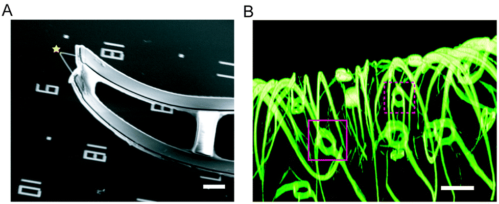 | ||
| Fig. 2 Flexible and three dimensional nanoelectronic devices. (A) Scanning electron microscopy image of a single kinked nanowire probe used for intracellular potential recording. The yellow star highlights the position of a field effect transistor. Scale bar, 5 μm. (B) Confocal fluorescence microscopy image of a macroporous nanoelectronic scaffold used for sensing from engineered tissues. Magenta boxes demarcate two field effect transistor devices. Scale bar, 20 μm. | ||
2.4. A new library of bio-orthogonal tools
One of the most important properties of semiconductor materials is the diverse range of configurations, allowing for integration with biological systems in a bio-orthogonal fashion.13,38 During the past several decades, many such materials have been designed and realized, including colloidal nanoparticles,39 semiconductor nanowires (NWs) and carbon nanotubes,40–42 with scale dependent properties distinct from the bulk. Among all semiconductor nanosystems, silicon based materials and devices are particularly important given that they are biocompatible and biodegradable.32,43,44 Nevertheless, other semiconductor components can be chemically engineered to reduce their cytotoxicities under physiological conditions.45,46 This diverse set of materials provides a wide range of nanoscopic “building blocks” that can be applied in a biological context leading to a host of possible applications, with some examples including nanoscale biosensors,23,24,28 drug delivery systems,38,47–49 intracellular pressure sensors50 and engineered tissue scaffolds.14In regard to diverse functionality through synthetic control, silicon nanowires (SiNWs) have been one of the most successful nanoscopic platforms. SiNW structures can be designed and synthetically realized with complex, yet controlled, modulations in composition, doping, defects, and even topography13,41,42 (Fig. 3A). Recent progress has also been observed in the synthesis of other meso- or nanostructured silicon materials, such as silicon ‘diatoms’51 (Fig. 3B) and nanoporous silicon membranes52 (Fig. 3C). This high degree of synthetic control enables the creation of building blocks with predictable physical properties and the assembly of hybrid or multicomponent functional materials in novel layouts and configurations, in turn allowing for the rational exploration of the silicon–biology interface,38 creating new opportunities and technologies for a library of bio-orthogonal tools.
 | ||
| Fig. 3 Complex silicon-based nanostructured materials. (A) Scanning electron microscopy image of a kinked nanowire; yellow arrow highlights the gold catalyst used for VLS growth. (B) A silicon ‘diatom’ synthesized by magnesium reduction. (C) A nanoporous silicon membrane used for molecular separation. B and C are adapted from ref. 51 and 52, respectively, with the permission from Nature Publishing Group. | ||
3. Silicon nanowire sensors for molecular biophysics studies
3.1. Study of molecule kinetics and activities
Nanowire field effect transistor based devices can be designed to examine protein dynamics with high precision at both an ensemble and a single protein level.24,30 Selective protein discrimination can be achieved by the modification of a detector's surface, in an analogous fashion to biomarker detection.24,28,29 When multiple binding domains are present on a single detector, this approach yields an ensemble measurement and can be used to examine kinetics information; however, this approach can also be adapted to the single protein level, reporting on processes such as folding and unfolding.53 To study single protein dynamics, only a single protein may be present on an individual detector. Achieving this can pose a significant challenge, but could be addressed through point defect methods as demonstrated in carbon nanotube based sensors.54,55 Single protein dynamics can offer insight into the different stages of the enzymatic process, such as protein specific turnover rates, and the cause of enzymatic deactivation at the single molecule level; information not readily available from ensemble measurements.3.2. DNA detection with NWFET pores
As the demand for DNA sequencing increases, new high-throughput methods are needed to reduce consumer prices and achieve faster sequencing rates. To meet this challenge, a variety of methods have been explored, including translocation through nanotube devices56 and solid state nanopore devices.57–59 The nanopore based platform is one of the most promising techniques, sequencing DNA by measuring the conductance through nanoscopic pores as DNA transports between two aqueous compartments.58,59 However, the membrane translocation speed, ∼1 μs per base, can be too fast for signal amplification in small ion currents and can result in the detection lag.60 One proposed solution is the use of NWFETs which can detect DNA in an analogous fashion to proteins and pathogens, but with faster temporal resolution. In 2011 the Lieber group demonstrated that NWFETs could potentially be configured as DNA sequencing devices when used in conjunction with a nanoscopic membrane pore,60 combining the advantages of both techniques.4. Silicon nanowire sensors for cellular biophysics studies
4.1. Extracellular electrical recordings
Monitoring extracellular electrical processes is important in understanding both intra- and intercellular signaling, or how cells communicate across large networks. To study these processes, multiplexed NW arrays have been used both on the single cell level and as detectors for clustered groups of cells, allowing for the spatially resolved detection, stimulation and inhibition of extracellular signal propagation.11,13 NW biosensors can interface with single cells extracellularly, which sense changes in electric field potential as ionic species transverse the cell membrane (Fig. 4A). Multiple NWFETs can also be arranged along different points in the culture allowing for measurement of signal transduction speeds.13 Moreover, because these nanowires can be placed within a confined region without apparent cross-talk, differences between long distance and short distance signaling can be discerned.11,13 So far, NWFETs have already been used to explore electrical signal propagation in neuronal cells and cardiomyocytes,11,13 although we note that they also hold potential in the study of several other cell types that use electrical signals as an activation mechanism.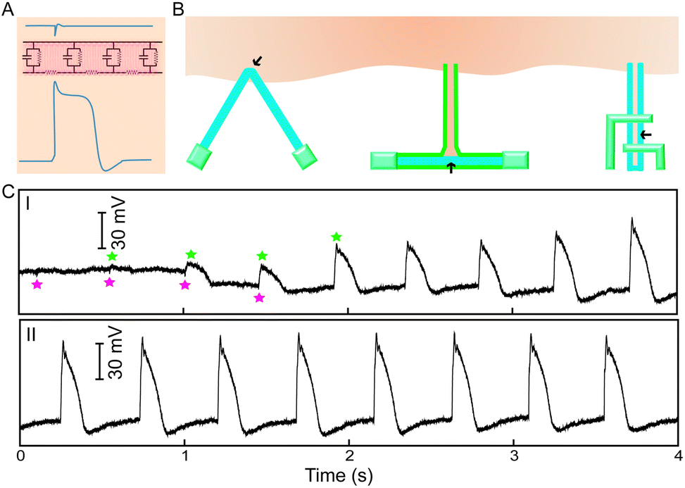 | ||
| Fig. 4 Intracellular electrical recording with field effect transistors. (A) Plot comparing the amplitude of intracellular (lower) vs. extracellular (upper) FET recordings, with shape ‘distortions’ due to the resistor–capacitor (RC) components from plasma membrane (middle). (B) Several FET configurations for intracellular recording. The black arrows indicate the sensing domains. (C) Electrical recording traces from a kinked nanowire probe as it transitions (I) from an extracellular (magenta stars) to intracellular (green stars) space, and (II) reaches an intracellular steady state. | ||
4.2. Intracellular electrical recordings
Lipid membranes serve as electrical barriers which attenuate transmembrane signal amplitude and produce signal distortions13 (Fig. 4A). As a result, extracellular sensors are limited in their capacity to detect intracellular signals. Recent progress has shown that NWFETs can be brought into contact with intracellular domains in order to directly record intracellular activities in a localized and tunable fashion, with three examples depicted in Fig. 4B: kinked NWFET,11 branched intracellular nanotube NWFET15 and active nanotube NWFET.16 The representative electrical recordings from a spontaneously beating cardiomyocyte using a kinked NWFET are shown in Fig. 4C.11This process is relatively non-invasive when compared to traditional intracellular recording probes such as voltage-sensitive optical dyes and single-terminal glass or carbon microelectrodes.13 Such electrodes are limited as intracellular species are exposed to the probe's electrolyte solution (Fig. 5A) and current is passed directly through the cytosol (Fig. 5B), both of which may induce irreversible changes to the cells, calling into question the physiological relevance of these recordings and preventing long-term non-invasive studies. Semiconductor devices are able to circumvent this by using a fundamentally different circuit configuration (Fig. 5C); processing cellular information without the need for direct communication with cellular ions thus minimizing junction impedance and cellular invasiveness issues.13
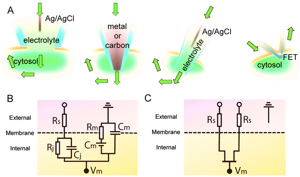 | ||
| Fig. 5 A comparison between conventional intracellular electrical recording tools and a kinked nanoscale field effect transistor (nanoFET) probe. (A) Four intracellular recordings are depicted: glass micropipette, metal or carbon micro/nanoelectrode, glass micropipette, and nanoFET (from left to right). The green arrows indicate the current flows. (B) and (C) are the equivalent circuits of the intracellular junctions established through conventional devices and nanoFET, respectively. Abbreviations: Cj, junction capacitance; Cm, membrane capacitance; Rs, series resistance; Rj, junction resistance; Rm, membrane resistance; Vm, intracellular potential. | ||
4.3. Electrical recordings from synthetic tissues
The use of semiconductors for recording electrical information can be further extended towards the development of synthetic tissues with embedded nanoelectronic sensory capabilities. In 2012, the Lieber and Kohane groups designed vascular nanoelectronic scaffold (nanoES) constructs for use in tissue-engineering blood vessels.14 Hybrid human aortic smooth muscle cell (HASMC) nanoES sheets were fabricated by culturing the cells on a 2D mesh nanoES with an agent that promotes natural ECM deposition on the mesh (Fig. 6A). The hybrids were then rolled into 3D tubular structures and allowed to mature (Fig. 6B). Micro-computed tomography (micro-CT) was used to visualize the distribution of the nanoES mesh in the tubular structure and it was shown that metal interconnects were regularly spaced (Fig. 6C, I) with at least four revolutions (Fig. 6C, II).14 The hybrid tissues were subsequently stained with hematoxylin–eosin and Masson-trichome stains revealing healthy 200 micron thick smooth muscle with embedded polymer (SU-8) ribbons from the nanoES confirming the 3D integration of the NWFET with the smooth muscle tissue (Fig. 6D). The ability to successfully integrate NW sensors into 3D tissues represents a new direction for merging nanoelectronics with biological systems including incorporating nanoscale stimulatory elements into the tissue-nanoES hybrids.13 With future engineering approaches, sensing capabilities could be broadened to address various disease states, in vitro (lab-on-a-chip, 3D tissue-based therapeutic assays) or in vivo. Cell or tissue interactions with nanoES could be fine-tuned by modification with cell growth determinants.47 The elements in nanoES could be expanded to incorporate nanoscale stimulators and stretchable designs35 to provide electrical and mechanical stimulation to enhance cell culture; in vivo these properties could provide functionalities such as pacing, and moduli that match those of host tissues. | ||
| Fig. 6 Nanoelectronics integrated into synthetic tissue. (A) (I) Photograph of a single HASMC sheet cultured with sodium L-ascorbate on a nanoES. (II) Zoomed-in view of the dashed area in (I), showing metallic interconnects macroscopically integrated with cellular sheet. (B) Photograph of the vascular construct after rolling into a tube and maturation in a culture chamber for 3 weeks. (C) (I) Micro-computed tomograph of a tubular construct segment. (II) Zoomed-in view of (I). Yellow arrows mark the individual nanowire FET-containing layers of the rolled construct. Scale bar, 1 mm. (D) (I) Hematoxylin & eosin and (II) Masson trichrome (collagen is blue) stained sections of nanoelectronic-HASMC hybrid (∼6 μm thick) cut perpendicular to the tube axis; lumen regions are labeled. Black arrows mark the positions of SU-8 ribbons of the nanoES. Scale bars, 50 μm. | ||
5. Outlook
As minimally invasive and highly sensitive detectors, nanoscale semiconductor devices offer a promising new approach to studying the behavior of electrical activity in a biological context. Notably, there are emerging challenges and opportunities in FET based electrical sensing of biological systems. For example, although pH sensing is readily achievable, the sensitivity for proteins and other macromolecules under physiological conditions need to be improved significantly with new operation schemes61 or surface chemistry.62 Additionally, FETs are currently limited to the detection of potential variations and charges, and there is still a significant need for ionic current sensing in order to understand more quantitatively the signaling of biological systems.63,64This mini-review has highlighted some of the key aspects that make semiconductors good detectors; however, there are many unexplored opportunities for also influencing the behavior of cells via electrical or optoelectronic stimulation. The mechanisms by which proteins sense voltage changes are diverse.65 Ion channels, for example, have a conserved, positively charged transmembrane region that moves in response to changes in membrane potential.65 Additionally, some G-protein coupled receptors possess a specific voltage-sensing motif while some membrane pumps and transporters use the ions that they transport across membranes to sense membrane voltage.65 The charged groups of proteins, their arrangements, local field strength, disposition and movements of the charges or dipoles can be variable; however, the final result is that changes in the electric field are transduced into a conformational change that alters the protein's function, thereby ultimately controlling a single cell's behavior.65 This important feature of proteins not only strongly indicates that the intracellular bioelectric networks may be very important in cell signaling (Fig. 1), but also that such protein responses can be controlled using localized electrical or optoelectronic stimulations through nanostructured semiconductor devices. This gives rise to the possibility of ‘Cyborg Cells’ and a technique based on the semiconductor analog of ‘optogenetics’,66–68 cells with internalized semiconducting materials capable of tunable behavior, controlled using external optical and electrical stimuli (Fig. 1).
Acknowledgements
BT acknowledges the financial support from National Science Foundation (NSF CAREER, Award Number 1254637) and Searle Scholars Foundation. RP acknowledges support from Interdisciplinary Scientist Training Program – T32 NIH Training grant (GM007281).References
- M. Levin, Semin. Cell Dev. Biol., 2009, 20, 543–556 CrossRef PubMed.
- M. Levin and C. G. Stevenson, in Annual Review of Biomedical Engineering, ed. M. L. Yarmush, 2012, vol. 14, pp. 295–323 Search PubMed.
- M. Levin, Bioelectromagnetics, 2003, 24, 295–315 CrossRef CAS PubMed.
- M. Cifra, J. Z. Fields and A. Farhadi, Prog. Biophys. Mol. Biol., 2011, 105, 223–246 CrossRef CAS PubMed.
- M. Cifra, J. Pokorny, D. Havelka and O. Kucera, Biosystems, 2010, 100, 122–131 CrossRef CAS PubMed.
- O. Kann and R. Kovacs, Am. J. Physiol. Cell Physiol., 2007, 292, C641–C657 CrossRef CAS PubMed.
- M. E. Spira and A. Hai, Nat. Nanotechnol., 2013, 8, 83–94 CrossRef CAS PubMed.
- C. Grewer, A. Gameiro, T. Mager and K. Fendler, in Annual Review of Biophysics, ed. K. A. Dill, 2013, vol. 42, pp. 95–120 Search PubMed.
- T. Knopfel, Nat. Rev. Neurosci., 2012, 13, 687–700 Search PubMed.
- A. Grinvald and R. Hildesheim, Nat. Rev. Neurosci., 2004, 5, 874–885 CrossRef CAS PubMed.
- B. P. Timko, T. Cohen-Karni, Q. Qing, B. Z. Tian and C. M. Lieber, Ieee Trans. Nanotechnol., 2010, 9, 269–280 CrossRef PubMed.
- B. Z. Tian and C. M. Lieber, Pure Appl. Chem., 2011, 83, 2153–2169 CrossRef CAS PubMed.
- B. Z. Tian and C. M. Lieber, in Annual Review of Analytical Chemistry, ed. R. G. Cooks and J. E. Pemberton, 2013, vol. 6, pp. 31–51 Search PubMed.
- B. Z. Tian, J. Liu, T. Dvir, L. H. Jin, J. H. Tsui, Q. Qing, Z. G. Suo, R. Langer, D. S. Kohane and C. M. Lieber, Nat. Mater., 2012, 11, 986–994 CrossRef CAS PubMed.
- X. J. Duan, R. X. Gao, P. Xie, T. Cohen-Karni, Q. Qing, H. S. Choe, B. Z. Tian, X. C. Jiang and C. M. Lieber, Nat. Nanotechnol., 2012, 7, 174–179 CrossRef CAS PubMed.
- R. X. Gao, S. Strehle, B. Z. Tian, T. Cohen-Karni, P. Xie, X. J. Duan, Q. Qing and C. M. Lieber, Nano Lett., 2012, 12, 3329–3333 CrossRef CAS PubMed.
- Q. Qing, S. K. Pal, B. Z. Tian, X. J. Duan, B. P. Timko, T. Cohen-Karni, V. N. Murthy and C. M. Lieber, Proc. Natl. Acad. Sci. U. S. A., 2010, 107, 1882–1887 CrossRef CAS PubMed.
- Z. Jiang, Q. Qing, P. Xie, R. X. Gao and C. M. Lieber, Nano Lett., 2012, 12, 1711–1716 CrossRef CAS PubMed.
- G. M. Whitesides, Nat. Biotechnol., 2003, 21, 1161–1165 CrossRef CAS PubMed.
- M. Leong, B. Doris, J. Kedzierski, K. Rim and M. Yang, Science, 2004, 306, 2057–2060 CrossRef PubMed.
- C. Brenner and M. Moulin, Circ. Res., 2012, 111, 1237–1247 CrossRef CAS PubMed.
- X. J. Duan, T. M. Fu, J. Liu and C. M. Lieber, Nano Today, 2013, 8, 351–373 CrossRef CAS PubMed.
- F. Patolsky, G. F. Zheng and C. M. Lieber, Nat. Protoc., 2006, 1, 1711–1724 CrossRef CAS PubMed.
- G. F. Zheng, F. Patolsky, Y. Cui, W. U. Wang and C. M. Lieber, Nat. Biotechnol., 2005, 23, 1294–1301 CrossRef CAS PubMed.
- Y. J. Hu, J. Xiang, G. C. Liang, H. Yan and C. M. Lieber, Nano Lett., 2008, 8, 925–930 CrossRef CAS PubMed.
- J. Xiang, W. Lu, Y. J. Hu, Y. Wu, H. Yan and C. M. Lieber, Nature, 2006, 441, 489–493 CrossRef CAS PubMed.
- G. MacBeath, Nat. Genet., 2002, 32, 526–532 CrossRef CAS PubMed.
- E. Stern, J. F. Klemic, D. A. Routenberg, P. N. Wyrembak, D. B. Turner-Evans, A. D. Hamilton, D. A. LaVan, T. M. Fahmy and M. A. Reed, Nature, 2007, 445, 519–522 CrossRef CAS PubMed.
- E. Stern, A. Vacic, N. K. Rajan, J. M. Criscione, J. Park, B. R. Ilic, D. J. Mooney, M. A. Reed and T. M. Fahmy, Nat. Nanotechnol., 2010, 5, 138–142 CrossRef CAS PubMed.
- X. X. Duan, Y. Li, N. K. Rajan, D. A. Routenberg, Y. Modis and M. A. Reed, Nat. Nanotechnol., 2012, 7, 401–407 CrossRef CAS PubMed.
- J. Yao, H. Yan and C. M. Lieber, Nat. Nanotechnol., 2013, 8, 329–335 CrossRef CAS PubMed.
- S. W. Hwang, H. Tao, D. H. Kim, H. Y. Cheng, J. K. Song, E. Rill, M. A. Brenckle, B. Panilaitis, S. M. Won, Y. S. Kim, Y. M. Song, K. J. Yu, A. Ameen, R. Li, Y. W. Su, M. M. Yang, D. L. Kaplan, M. R. Zakin, M. J. Slepian, Y. G. Huang, F. G. Omenetto and J. A. Rogers, Science, 2012, 337, 1640–1644 CrossRef CAS PubMed.
- R. C. Webb, A. P. Bonifas, A. Behnaz, Y. H. Zhang, K. J. Yu, H. Y. Cheng, M. X. Shi, Z. G. Bian, Z. J. Liu, Y. S. Kim, W. H. Yeo, J. S. Park, J. Z. Song, Y. H. Li, Y. G. Huang, A. M. Gorbach and J. A. Rogers, Nat. Mater., 2013, 12, 938–944 CrossRef CAS PubMed.
- D. H. Kim, N. S. Lu, R. Ghaffari, Y. S. Kim, S. P. Lee, L. Z. Xu, J. A. Wu, R. H. Kim, J. Z. Song, Z. J. Liu, J. Viventi, B. de Graff, B. Elolampi, M. Mansour, M. J. Slepian, S. Hwang, J. D. Moss, S. M. Won, Y. G. Huang, B. Litt and J. A. Rogers, Nat. Mater., 2011, 10, 316–323 CrossRef CAS PubMed.
- D. H. Kim, N. S. Lu, R. Ma, Y. S. Kim, R. H. Kim, S. D. Wang, J. Wu, S. M. Won, H. Tao, A. Islam, K. J. Yu, T. I. Kim, R. Chowdhury, M. Ying, L. Z. Xu, M. Li, H. J. Chung, H. Keum, M. McCormick, P. Liu, Y. W. Zhang, F. G. Omenetto, Y. G. Huang, T. Coleman and J. A. Rogers, Science, 2011, 333, 838–843 CrossRef CAS PubMed.
- J. A. Rogers, M. G. Lagally and R. G. Nuzzo, Nature, 2011, 477, 45–53 CrossRef CAS PubMed.
- J. Viventi, D. H. Kim, L. Vigeland, E. S. Frechette, J. A. Blanco, Y. S. Kim, A. E. Avrin, V. R. Tiruvadi, S. W. Hwang, A. C. Vanleer, D. F. Wulsin, K. Davis, C. E. Gelber, L. Palmer, J. Van der Spiegel, J. Wu, J. L. Xiao, Y. G. Huang, D. Contreras, J. A. Rogers and B. Litt, Nat. Neurosci., 2011, 14, 1599-U1138 CrossRef PubMed.
- D. Fine, A. Grattoni, R. Goodall, S. S. Bansal, C. Chiappini, S. Hosali, A. L. van de Ven, S. Srinivasan, X. W. Liu, B. Godin, L. Brousseau, I. K. Yazdi, J. Fernandez-Moure, E. Tasciotti, H. J. Wu, Y. Hu, S. Klemm and M. Ferrari, Adv. Healthc. Mater., 2013, 2, 632–666 CrossRef CAS PubMed.
- Y. Yin and A. P. Alivisatos, Nature, 2005, 437, 664–670 CrossRef CAS PubMed.
- J. T. Hu, T. W. Odom and C. M. Lieber, Acc. Chem. Res., 1999, 32, 435–445 CrossRef CAS.
- Y. Li, F. Qian, J. Xiang and C. M. Lieber, Mater. Today, 2006, 9, 18–27 CrossRef CAS.
- W. Lu and C. M. Lieber, J. Phys. D: Appl. Phys., 2006, 39, R387–R406 CrossRef CAS.
- M. C. Cassidy, H. R. Chan, B. D. Ross, P. K. Bhattacharya and C. M. Marcus, Nat. Nanotechnol., 2013, 8, 363–368 CrossRef CAS PubMed.
- E. Tasciotti, X. W. Liu, R. Bhavane, K. Plant, A. D. Leonard, B. K. Price, M. M. C. Cheng, P. Decuzzi, J. M. Tour, F. Robertson and M. Ferrari, Nat. Nanotechnol., 2008, 3, 151–157 CrossRef CAS PubMed.
- M. A. Dobrovolskaia, D. R. Germolec and J. L. Weaver, Nat. Nanotechnol., 2009, 4, 411–414 CrossRef CAS PubMed.
- A. E. Nel, L. Madler, D. Velegol, T. Xia, E. M. V. Hoek, P. Somasundaran, F. Klaessig, V. Castranova and M. Thompson, Nat. Mater., 2009, 8, 543–557 CrossRef CAS PubMed.
- T. Dvir, B. P. Timko, D. S. Kohane and R. Langer, Nat. Nanotechnol., 2011, 6, 13–22 CrossRef CAS PubMed.
- B. P. Timko, T. Dvir and D. S. Kohane, Adv. Mater., 2010, 22, 4925–4943 CrossRef CAS PubMed.
- A. K. Shalek, J. T. Robinson, E. S. Karp, J. S. Lee, D.-R. Ahn, M.-H. Yoon, A. Sutton, M. Jorgolli, R. S. Gertner, T. S. Gujral, G. MacBeath, E. G. Yang and H. Park, Proc. Natl. Acad. Sci. U. S. A., 2010, 107, 1870–1875 CrossRef CAS PubMed.
- R. Gomez-Martinez, A. M. Hernandez-Pinto, M. Duch, P. Vazquez, K. Zinoviev, E. J. de la Rosa, J. Esteve, T. Suarez and J. A. Plaza, Nat. Nanotechnol., 2013, 8, 517–521 CrossRef CAS PubMed.
- Z. H. Bao, M. R. Weatherspoon, S. Shian, Y. Cai, P. D. Graham, S. M. Allan, G. Ahmad, M. B. Dickerson, B. C. Church, Z. T. Kang, H. W. Abernathy, C. J. Summers, M. L. Liu and K. H. Sandhage, Nature, 2007, 446, 172–175 CrossRef CAS PubMed.
- C. C. Striemer, T. R. Gaborski, J. L. McGrath and P. M. Fauchet, Nature, 2007, 445, 749–753 CrossRef CAS PubMed.
- Y. K. Choi, I. S. Moody, P. C. Sims, S. R. Hunt, B. L. Corso, I. Perez, G. A. Weiss and P. G. Collins, Science, 2012, 335, 319–324 CrossRef CAS PubMed.
- B. R. Goldsmith, J. G. Coroneus, V. R. Khalap, A. A. Kane, G. A. Weiss and P. G. Collins, Science, 2007, 315, 77–81 CrossRef CAS PubMed.
- S. Sorgenfrei, C. Y. Chiu, R. L. Gonzalez, Y. J. Yu, P. Kim, C. Nuckolls and K. L. Shepard, Nat. Nanotechnol., 2011, 6, 125–131 CrossRef PubMed.
- J. Goldberger, R. Fan and P. D. Yang, Acc. Chem. Res., 2006, 39, 239–248 CrossRef CAS PubMed.
- B. M. Venkatesan and R. Bashir, Nat. Nanotechnol., 2011, 6, 615–624 CrossRef CAS PubMed.
- D. Branton, D. W. Deamer, A. Marziali, H. Bayley, S. A. Benner, T. Butler, M. Di Ventra, S. Garaj, A. Hibbs, X. H. Huang, S. B. Jovanovich, P. S. Krstic, S. Lindsay, X. S. S. Ling, C. H. Mastrangelo, A. Meller, J. S. Oliver, Y. V. Pershin, J. M. Ramsey, R. Riehn, G. V. Soni, V. Tabard-Cossa, M. Wanunu, M. Wiggin and J. A. Schloss, Nat. Biotechnol., 2008, 26, 1146–1153 CrossRef CAS PubMed.
- D. Deamer, in Annual Review of Biophysics, ed. D. C. Rees, K. A. Dill and J. R. Williamson, 2010, vol. 39, pp. 79–90 Search PubMed.
- P. Xie, Q. H. Xiong, Y. Fang, Q. Qing and C. M. Lieber, Nat. Nanotechnol., 2012, 7, 119–125 CrossRef CAS PubMed.
- G. S. Kulkarni and Z. H. Zhong, Nano Lett., 2012, 12, 719–723 CrossRef CAS PubMed.
- J. M. Buriak, Chem. Rev., 2002, 102, 1271–1308 CrossRef CAS PubMed.
- G. Buzsaki, C. A. Anastassiou and C. Koch, Nat. Rev. Neurosci., 2012, 13, 407–420 CrossRef CAS PubMed.
- B. Reid, R. Nuccitelli and M. Zhao, Nat. Protoc., 2007, 2, 661–669 CrossRef CAS PubMed.
- F. Bezanilla, Nat. Rev. Mol. Cell Biol., 2008, 9, 323–332 CrossRef CAS PubMed.
- T. I. Kim, J. G. McCall, Y. H. Jung, X. Huang, E. R. Siuda, Y. H. Li, J. Z. Song, Y. M. Song, H. A. Pao, R. H. Kim, C. F. Lu, S. D. Lee, I. S. Song, G. Shin, R. Al-Hasani, S. Kim, M. P. Tan, Y. G. Huang, F. G. Omenetto, J. A. Rogers and M. R. Bruchas, Science, 2013, 340, 211–216 CrossRef CAS PubMed.
- L. Martiradonna, Nat. Mater., 2013, 12, 472–472 CrossRef.
- K. Deisseroth, Nat. Methods, 2011, 8, 26–29 CrossRef CAS PubMed.
| This journal is © The Royal Society of Chemistry 2014 |