A simple and inexpensive technique for PDMS/silicon chip alignment with sub-μm precision
R.
Sivakumarasamy
a,
K.
Nishiguchi
b,
A.
Fujiwara
b,
D.
Vuillaume
a and
N.
Clément
*a
aIEMN-CNRS, Avenue Poincaré, Cité Scientifique, 59652 Villeneuve d'Ascq, France. E-mail: nicolas.clement@iemn.univ-lille1.fr; Tel: +33 320197932
bNTT Basic Research Laboratories, 3-1 Morinosato Wakamiya, Atsugi, Kanagawa 243-0198, Japan
First published on 24th September 2013
Abstract
This paper describes a novel simple and inexpensive assembly technique with highly accurate alignment of a polydimethylsiloxane (PDMS) layer on a silicon chip for hybrid microfluidic/electronic applications. It is based on strong electrostatic adhesion of a 200 μm thick and dense layer of PDMS onto a metallic cylindrical tool mechanically fixed to an optical microscope. A 2 mm hole in the tool allows precise alignment of the PDMS layer, 10 μm from the surface, without the usage of any lubricant. The same tool is used for PDMS bonding in a well-controlled manner. This technique is compatible with wafer scale alignment. A very precise consideration of the PDMS shrinkage ratio, reduced by 50% for thin layers, enables a misalignment range of less than 1 μm in the experiments.
Introduction
Optically transparent materials, such as glass, epoxy resin, or acrylic resin, are widely used for microfluidic devices.1–3 Among those materials, polydimethylsiloxane (PDMS) is especially effective for biological studies, because of its high biocompatibility, inexpensiveness, flexibility and optical transparency.4,5Microfluidic devices made of PDMS have generally a single layer and are bonded to a glass substrate.6,7 However, channels with complex structures are emerging to improve the performance, the functionality and the packing density of the devices.8–12 In particular, hybrid PDMS microfluidic devices combined with highly integrated sensors on silicon chips13–16 will require inevitably alignment precision in the micrometer range or lower. Actually, such an alignment precision level is only reached for three-dimensional glass structures realized by laminating two or three thin-glass substrates.17,18 The tools for automatic alignment use robotic microhandling and position measurement by optical techniques to achieve a highly accurate alignment.19–21 However, these tools are not suitable for devices composed of PDMS substrates, because of the elasticity of PDMS. The deflection caused by the elastic behaviour makes it difficult to hold the substrates and to adjust the gap size between them. Furthermore, the sticky surface of the PDMS substrate leads to misalignment when the held substrates are dismounted from the tool. Therefore, free-hand alignment using alignment marks is generally required to assemble microfluidic devices made of laminated PDMS substrates.22 As a consequence, although PDMS-based technology appears mature, there is still a need for PDMS alignment techniques, by preference simple and inexpensive,23 with micrometric or sub-micrometric precision. Recently, a novel assembly technique with semi-automatic alignment for the PDMS substrate has enabled a misalignment average range of less than 1.9 μm,24 although with 7.9 μm standard deviation. This technique is only available for alignment of two PDMS layers. So far, alignment precision for PDMS/silicon chips in the range of 10 μm has been reported.25 In that case, the shrinkage ratio of PDMS has to be considered (not in the case for PDMS–PDMS bonding), which adds another source of misalignment. The optical camera has to be used in sole reflection mode and the optimized focus for alignment is only obtained for thin PDMS layers. Nevertheless, lubricants usually used for PDMS alignment26 induce PDMS deformation for very thin PDMS layers.
In this paper, we propose a new technique based on the electrostatic adhesion force of a 200 μm thick and dense layer of PDMS, that is stronger than its weight, onto a simple metallic cylindrical tool mechanically fixed to an optical microscope. We point out that the PDMS shrinkage ratio must be precisely estimated with ppm error for perfect alignment on silicon. Interestingly, this ratio is drastically reduced for thin spin coated PDMS layers. No lubricant coating was necessary with our technique. We evaluated the misalignment error from the patterned silicon chip.
Principles and methods
A. Alignment and bonding tool
The alignment tool used in this study is based on the simple observation that adhesion of a 200 μm thick layer of PDMS to a metallic surface is larger than its weight (Fig. 1).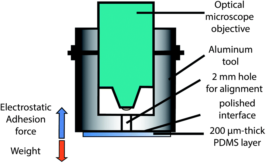 | ||
| Fig. 1 Schematic view of the aluminum tool used for PDMS alignment fixed to an optical microscope. The electrostatic adhesion force of a 200 μm thick layer of PDMS is larger than its weight. In contrast to usual methods, no lubricant is necessary with this technique. | ||
The inner diameter of the cylinder corresponds to that of the optical microscope objective. The outer diameter depends on the sample size (typically 2 or 3 inches). In particular, for large PDMS surfaces, it is important to polish the aluminum tool and keep it clean to get high enough electrostatic adhesion. We selected a 5× zoom objective in order to see enough alignment marks and correct precisely the tilt angle.
B. Fabrication
Precise alignment can be done within few minutes using the above described tool. The fabrication process of the thin PDMS layer is slightly different from the conventional process. The only difference is that the ratio of the PDMS curing agent to the base was changed from 1![[thin space (1/6-em)]](https://www.rsc.org/images/entities/char_2009.gif) :10 (standard) to 1:3, to ensure that the 200 μm thick PDMS was dense enough for easy manipulation. Microfluidic channels were fabricated by using conventional soft lithography techniques.27–29
:10 (standard) to 1:3, to ensure that the 200 μm thick PDMS was dense enough for easy manipulation. Microfluidic channels were fabricated by using conventional soft lithography techniques.27–29
C. Alignment process
Fig. 2 shows the whole alignment process. The lower silicon substrate was patterned with aluminum marks shown in Fig. 2a. Typically, 150 μm × 150 μm square pads were enough for fast positioning of PDMS above the wafer. Smaller patterns (30 μm) were used for precise alignment. The pattern on PDMS (after demolding) matches with the pattern on silicon.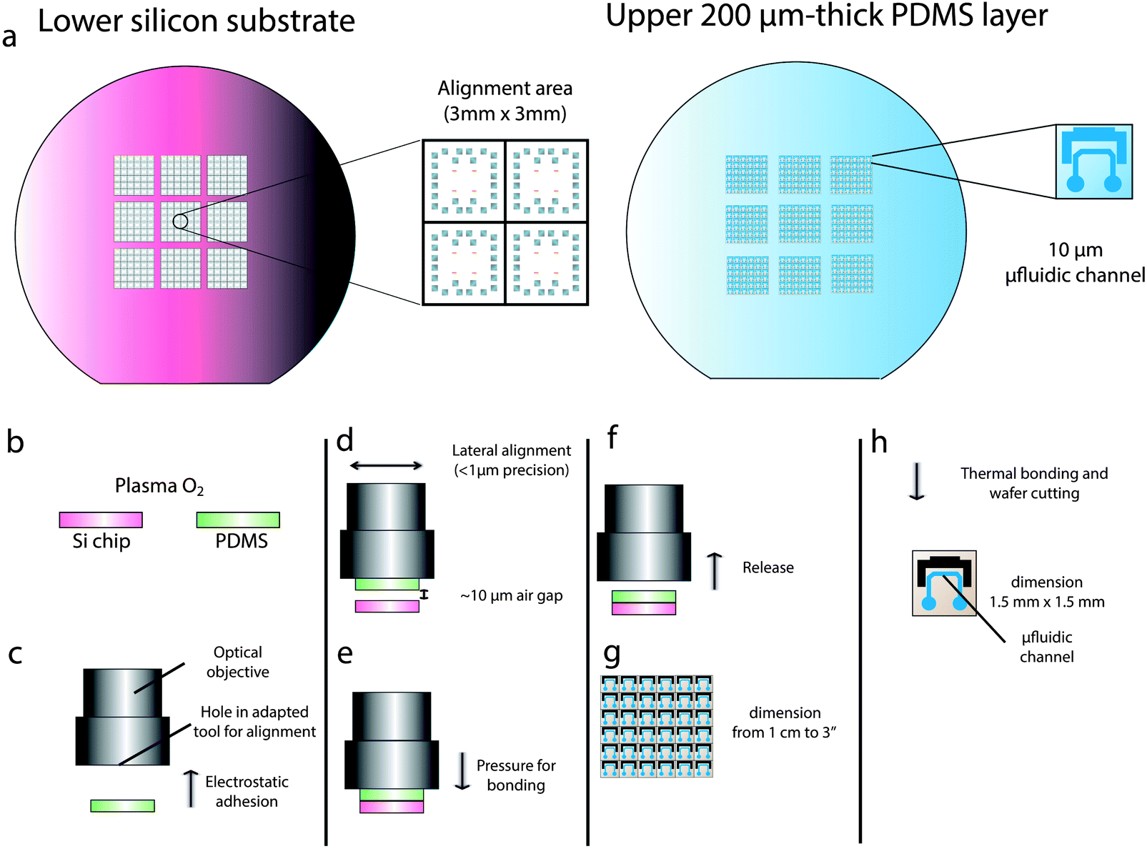 | ||
| Fig. 2 (a) Schematic view of the patterned silicon wafer and unmold PDMS layer. (b) Both Si and PDMS substrates are exposed to O2 plasma. (c) PDMS layer is put into contact with the aluminum tool (usually before mounting the tool). (d) PDMS/silicon alignment. (e) Vertical displacement of the tool for bonding. (f) The tool is released. (g) Aligned samples are typically between 1 cm and 3′′. (h) Chip can eventually be cut into small LoCs after thermal bonding and wafer cutting. | ||
Oxygen plasma treatment for permanent bonding was similar to the conventional technique. An oxidation of PDMS and silicon substrates by oxygen plasma treatment (Fig. 2b) leads to strong intermolecular bonds.30 The PDMS layer was put into contact with the aluminum tool by electrostatic adhesion (Fig. 2c). Alignment was performed after focusing by micrometric lateral and tilt angle positioning (Fig. 2d). Usually, lubricants, such as water, ethanol, or methanol, are used to reduce the effect of the sticky surface.22 However, substrate deformation caused by the expanding gas of the lubricant and misalignment during evaporation are typical drawbacks. No lubricant was necessary with our technique. After proper alignment, only a vertical translation was used to put into contact both substrates and the pressure was applied until observation of proper contact between both layers (Fig. 2e). Then, the tool was released (Fig. 2f). Because both PDMS and silicon were plasma treated before contact, the bonding strength of both layers becomes larger than the electrostatic force of PDMS/aluminium and PDMS remains attached to the silicon surface. Typical dimensions of both silicon and PDMS substrates vary between 1 cm and 3′′ (Fig. 2g). After thermal treatment (120 °C) for permanent bonding, silicon wafer can be cut into pieces with a diamond tool.
D. Shrinkage ratio
Shrinkage of PDMS occurs when it is cured; this is a problem related to the alignment between the PDMS layer and the rigid substrate during the wafer-level processing. S.W. Lee and S.S. Lee have measured experimentally the 2D shrinkage ratio of PDMS under various curing conditions including the temperature, thickness, and mixing ratio of the curing agent and the diluent. Unfortunately, they have only estimated it for thick PDMS layers (>1 mm). Furthermore, the shrinkage ratio precision was not enough for the alignment precision required in our study. As a consequence, we evaluated the shrinkage ratio of thin PDMS layers and obtained unexpected results that will be discussed below. Several iterations have been performed to reach the sufficient precision.Experimental details
A. Alignment tool
Fig. 3 shows the aluminum 2′′ alignment tool used in this study. It was fixed to a standard optical microscope (Mitutoyo FS110 Inspection Microscope) with a large focal length. The rotating plateau is used for tilt angle correction.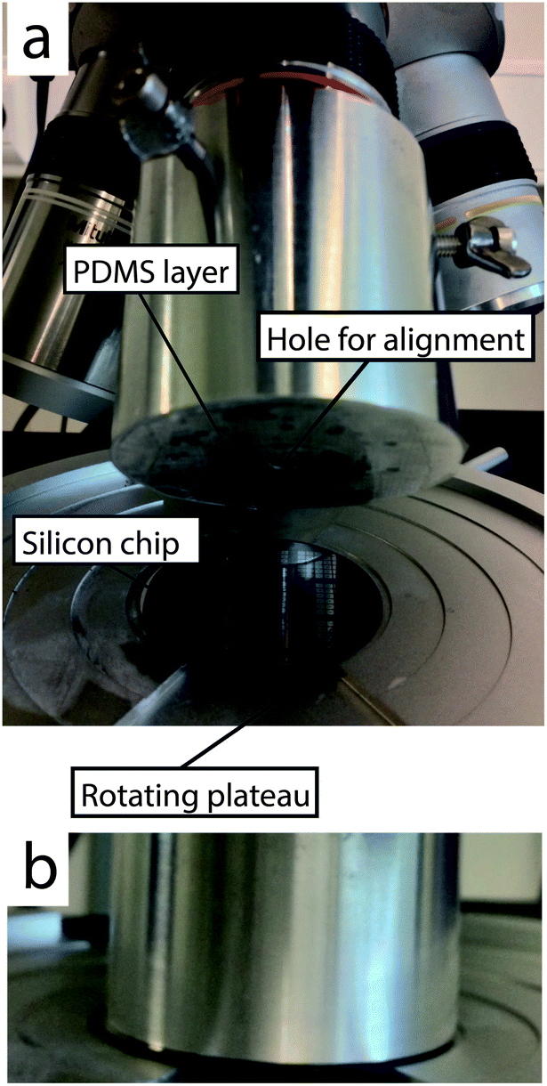 | ||
| Fig. 3 Picture of the tool before (a) and during (b) alignment. | ||
B. PDMS fabrication
For PDMS device fabrication, the uncured PDMS was spin-coated at 300 rpm for 30 s with an acceleration rate of 100 rpm. It was then cured in two steps: (i) at 65 °C for 20 min in contact with a hot plate, and (ii) in a convection oven at 120 °C for one hour. Oxygen plasma treatment before alignment was done at 0.7 mbar, 120 W, for 90 s.Silicon mold. S1818 resist (Microposit©) was spin-coated at 2500 rpm with an acceleration of 1000 rpm for 12 s. Silicon was etched using reactive ion etching (RIE). The gases used for the RIE process were SF6 and O2. The gas used for passivation was C4F8. The flow rates of SF6, O2, and C4F8 were 450, 45, and 100 standard cm3 per minute (sccm), respectively. The coil power was 1000 W. RIE had an approximate etch rate of 4 μm min−1. The etching time required to achieve a trench depth of 44 μm was 10 min. After etching the wafers, we examined the microstructures on the wafers by optical microscopy. We stripped the remaining photoresist from the silicon wafer by immersing the wafer in EKC 265 at 60 °C for 30 min, followed by immersion in acetone and isopropanol for 5 min each.
Results and discussion
A. Shrinkage ratio
A schematic view of the protocol used for PDMS shrinkage ratio estimation is shown in Fig. 4. It is obtained after alignment of both layers by evaluation of the misalignment ΔD at corners of 150 μm Al pads located at D ∼ 1 cm from each other to improve sensitivity ([D + 2ΔD]/D). Table 1 shows the results of the shrinkage ratio obtained at a curing temperature of 120 °C for 1 h. Interestingly, the shrinkage ratio for our 200 μm thick PDMS layer was only 1.0263% whereas 1.94% was previously reported for 1.2 mm thick PDMS (50% decrease).25 The reason why thin, spin coated PDMS has a lower shrinkage ratio might be due to the loss of elasticity after baking on the mold. A reduced shrinkage ratio is surely an advantage for perfect alignment since it implies a reduced sample to sample dispersion. Indeed, no dispersion (<1 μm/1 cm) has been observed with thin PDMS layers. After several iterations, we obtained a ratio of 1.0223%. Such a precise estimation is mandatory for reaching sub-μm misalignment error. This value slightly changes with the curing agent to base ratio (Table 1).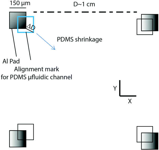 | ||
| Fig. 4 Schematic view of the protocol used for shrinkage ratio estimation. | ||
B. Alignment
Misalignment error is obtained from the distance ΔD between the corner of 150 μm aluminum pads and the equivalent pattern on PDMS (Fig. 4). Fig. 5a and b show optical microscopy images at different zoom scales of aligned PDMS microfluidic channels (10 μm large) on aluminum electrodes. The average and standard deviation of misalignment error obtained from 36 devices located at 2, 4 and 6 mm from the center are shown in Table 2. Close to the center (diameter below 5 mm), alignment and standard deviations, measured with a Leica Microsystem (DM-4000-M), are nearly perfect. These values increase up to 3.6 μm (0.1 μm standard deviation) only in the X direction and at the side of 1.5 cm chips, but remain better than the previously reported misalignment error on silicon (10 μm in ref. 25) and even on PDMS24 (1.9 μm with 7.9 μm standard deviation). Further improvement in alignment precision could be obtained by using our alignment tool with a larger optical zoom, but probably misalignment error would be increased far from the center. The misalignment error on the X axis might be due to the non-uniform pressure applied on the PDMS at the bonding stage. Considering the resolution limit of mask patterning for soft lithography, the misalignment range is already highly accurate. We believe that reproducible sub-micrometric alignment is obtained thanks to the well-controlled shrinkage ratio of thin PMDS layers. In usual processes, misalignment occurs just after alignment due to unexpected shock, vibrations and tilt while waiting for the stabilization of the intermolecular bonding. However, with our technique, only a vertical axis displacement was performed for applying pressure and releasing the tool and such an effect has not been observed. The lack of a lubricant is probably the reason.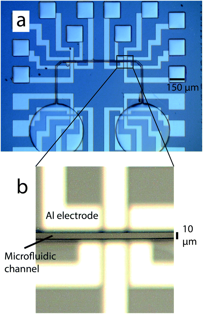 | ||
| Fig. 5 (a) Optical microscopy image of the aligned PDMS microfluidic channel. (b) Zoom-in view of (a). | ||
| PDMS thickness | Distance from the center | 2 mm | 4 mm | 6 mm |
|---|---|---|---|---|
| 160 μm | Mean (μm) | 0.19 | 1.66 | 3.66 |
| Standard deviation (μm) | 0.05 | 0.12 | 0.1 | |
| 350 μm | Mean (μm) | 0.32 | 2.22 | 4.15 |
| Standard deviation (μm) | 0.03 | 0.12 | 0.09 |
Conclusions
In this paper, we have shown that thin PDMS layers are of great advantage for precise alignment because the shrinkage ratio is reduced by 50% and the electrostatic adhesion force is larger than the weight of the PDMS layer. This has been considered for designing a dedicated tool for fast and easy PDMS alignment with high throughput. It will enable the replacement of resist microbaths14,31 aligned on silicon nanosensors with perfectly aligned PDMS microfluidic channels. This technique is not only the first step toward merging large scale integration (LSI) and microfluidic LSI (mLSI), but can also be used for PDMS–PDMS alignment with high accuracy and reproducibility.Acknowledgements
The authors would like to thank D. Troadec for discussion, J.M. Mallet for fabrication of the tool and Nord-Pas de Calais council and Lille University for funding (SINGLEMOL and BQR).Notes and references
- H. Craighead, Nature, 2006, 442, 387–393 CrossRef CAS PubMed.
- B. H. Weigl, R. L. Bardell and C. R. Cabrera, Adv. Drug Delivery Rev., 2003, 55, 349–377 CrossRef CAS.
- F. Kurth, K. Eyer, A. Franco-Obregon and P. S. Dittrich, Curr. Opin. Chem. Biol., 2012, 400–408 CrossRef CAS PubMed.
- E. Leclerc, Y. Sakai and T. Fujii, Biomed. Microdevices, 2003, 5, 109–114 CrossRef CAS.
- D. Armani, C. Liu and N. Aluru, Re-configurable fluid circuits by elastomer micromachining, Orlando, FL, 1999 Search PubMed.
- C. S. Effenhauser, G. J. Bruin, A. Paulus and M. Ehrat, Anal. Chem., 1997, 69, 3451–3457 CrossRef CAS PubMed.
- M. Seki, R. Aoyama, J. W. Hong, T. Fujii and I. Endo, Multiple diagnostic analyses by enzymatic and chemical reaction on a PDMS microchip, Lyon, 2000 Search PubMed.
- M. Yu, Q. Wang, J. E. Patterson and A. T. Wooley, Anal. Chem., 2011, 83, 3541–3547 CrossRef CAS PubMed.
- T. Thorsen, S. J. Maerkl and S. R. Quake, Science, 2002, 298, 580–584 CrossRef CAS PubMed.
- K. Gerasopoulos, M. McCarthy, E. Royston, J. N. Culver and R. Ghodssi, J. Micromech. Microeng., 2008, 18, 1–8 CrossRef.
- K. S. Lee, P. Boccazzi, A. J. Sinkey and R. J. Ram, Lab Chip, 2011, 11, 1856–1863 RSC.
- L. K. Chin, J. Q. Yu, Y. Fu, T. Yu, A. Q. Liu and K. Q. Luo, Lab Chip, 2011, 11, 257–262 RSC.
- N. Clément, K. Nishiguchi, A. Fujiwara and D. Vuillaume, Nat. Commun, 2012, 1, 92 CrossRef PubMed.
- N. Clément, K. Nishiguchi, J.-F. Dufrêche, D. Guérin, A. Fujiwara and D. Vuillaume, Nano Lett., 2013, 13, 3903 CrossRef PubMed.
- G. Larrieu and X.-L. Han, Vertical nanowire array-based field effect transistors for ultimate scaling, Nanoscale, 2013, 5, 2437–2441 RSC.
- S. Salomon, T. Leïchlé, D. Dezest, F. Seichepine, S. Guillon, C. Thibault, C. Vieu and L. Nicu, Nanotechnology, 2012, 23, 495501–495506 CrossRef CAS PubMed.
- A. Grosse, M. Grewe and H. Fouckhardt, J. Micromech. Microeng., 2001, 11, 257–262 CrossRef CAS.
- A. Daridon, V. Fascio, J. Lichtenberg, R. Wutrich, H. Langren, E. Verpoorte and N. F. de Rooji, Anal. Chem., 2001, 371, 261–269 CrossRef CAS.
- M. M. R. Howlader, A. Yamauchi and T. Suga, J. Electrochem. Soc., 2004, 151, G461–G467 CrossRef CAS PubMed.
- H. Takagi and R. Maeda, J. Micromech. Microeng., 2005, 15, 290–295 CrossRef CAS.
- M. M. R. Howlader, A. Yamauchi and T. Suga, J. Micromech. Microeng., 2011, 21, 1–10 CrossRef.
- K. Hosokawa and R. Maeda, J. Micromech. Microeng., 2000, 10, 415–420 CrossRef CAS.
- http://blogs.rsc.org/chipsandtips/2011/08/17/a-novel-technique-for-aligning-multiple-microfluidic-devices/ .
- K. Mogi and T. Fujii, Lab Chip, 2013, 13, 1044 RSC.
- S. W. Lee and S. S. Lee, Microsyst. Technol., 2008, 14, 205 CrossRef CAS.
- K. Mogi and T. Fuji, J. Micromech. Microeng., 2010, 20, 055015 CrossRef.
- T. Fuji, Microelectron. Eng., 2002, 61–62, 907–914 CrossRef.
- G. M. Whitesides, Abstracts of Papers of the American Chemical Society, 1996, 212, 31-Inor Search PubMed.
- G. M. Whitesides, E. Ostuni, S. Takayama, X. Jiang and D. Ingber, Annu. Rev. Biomed. Eng., 2001, 3, 335–373 CrossRef CAS PubMed.
- A. D. Shantanu Bhattacharya, J. M. Berg and S. Gangopadhyay, J. Microelectromech. Syst., 2005, 14, 590–597 CrossRef.
- N. Clément, K. Nishiguchi, J.-F. Dufrêche, D. Guérin, A. Fujiwara and D. Vuillaume, Appl. Phys. Lett., 2011, 98, 014104–014107 CrossRef.
| This journal is © The Royal Society of Chemistry 2014 |