
 Open Access Article
 This Open Access Article is licensed under a
 Creative Commons Attribution 3.0 Unported Licence
Screen-printed back-to-back electroanalytical sensors†
Jonathan P.
Metters
,
Edward P.
Randviir
and
Craig E.
Banks
*
Faculty of Science and Engineering, School of Chemistry and the Environment, Division of Chemistry and Environmental Science, Manchester Metropolitan University, Chester Street, Manchester M15 GD, Lancs, UK. E-mail: c.banks@mmu.ac.uk; Web: http://www.craigbanksresearch.com Fax: +44 (0)1612476831; Tel: +44 (0)1612471196
First published on 17th September 2014
Abstract
We introduce the concept of screen-printed back-to-back electroanalytical sensors where in this facile and generic approach, screen-printed electrodes are printed back-to-back with a common electrical connection to the two working electrodes with the counter and reference electrodes for each connected in the same manner as a normal “traditional” screen-printed sensor would be. This approach utilises the usually redundant back of the screen-printed sensor, converting this “dead-space” into a further electrochemical sensor which results in improvements in the analytical performance. In the use of the back-to-back design, the electrode area is consequently doubled with improvements in the analytical performance observed with the analytical sensitivity (gradient of a plot of peak height/analytical signal against concentration) doubling and the corresponding limit-of-detection being reduced. We also demonstrate that through intelligent electrode design, a quadruple in the observed analytical sensitivity can also be realised when double microband electrodes are used in the back-to-back configuration as long as they are placed sufficiently apart such that no diffusional interaction occurs. Such work is generic in nature and can be facilely applied to a plethora of screen-printed (and related) sensors utilising the commonly overlooked redundant back of the electrode providing facile improvements in the electroanalytical performance.
1. Introduction
Electroanalytical sensors find widespread use in a plethora of areas and have been an important field for research and development over recent years. Originally such sensors were used with mercury-based electrodes such as the dropping mercury electrode through to graphitic and metallic macroelectrodes modified with mercury films. Currently used macroelectrodes include edge plane and basal plane constructed from highly ordered pyrolytic graphite and glassy carbon and boron-doped diamond electrode which can be utilised as either bare (unmodified) or modified with electrocatalytic moieties or micro- and nano- materials such as carbon nanotubes,1–3 C60![[thin space (1/6-em)]](https://www.rsc.org/images/entities/char_2009.gif) 4 and graphene5–7 to name just a few examples. Such new developments in the type/construction of electrodes have brought about new types of sensors for the detection of a plethora of analytes in a range of sample matrixes. Electrochemists are always searching for the next generation of electrode materials in order to be analytically sensitive and selective to the target analyte. Other approaches, instead of exploring the composition/type of the electrode are to change the geometric shape, such as scaling down the size of the electrode substrates from that of a macroelectrode to a micro- or nano-electrode, where due to the physical change in size, mass transport processes change from linear/planar to that of convergent/radial diffusion which results in a quantitative change in the electroanalytical signal.
4 and graphene5–7 to name just a few examples. Such new developments in the type/construction of electrodes have brought about new types of sensors for the detection of a plethora of analytes in a range of sample matrixes. Electrochemists are always searching for the next generation of electrode materials in order to be analytically sensitive and selective to the target analyte. Other approaches, instead of exploring the composition/type of the electrode are to change the geometric shape, such as scaling down the size of the electrode substrates from that of a macroelectrode to a micro- or nano-electrode, where due to the physical change in size, mass transport processes change from linear/planar to that of convergent/radial diffusion which results in a quantitative change in the electroanalytical signal.
One of the problems often overlooked when considering electrochemical systems is that typically electroanalytical systems are developed to target analytes and very often the consideration for transferring the protocol from the laboratory in to the field is ignored. Screen-printing and related techniques are routinely used to produce a range of electrochemical sensing platforms and due to their scales of economy, low cost electrodes are realised which are reproducible and can be used as a single-use sensor. This is particularly useful when the electroanalytical protocol is intended to be implemented into third world countries where the realisation of low cost, reliable sensors is imperative for applications such as water quality testing as in such analytical environments where electrode “fouling” or passivation of electrochemical sensors is an issue. This typically occurs in real matrices such as in the case of heavy metal monitoring in water samples where biological components can adsorb on to the electrode surface and detrimentally affect the electroanalytical measurement and hence reduce the sensitivity of the electrochemical protocol, sometimes preventing measurement altogether. When solid electrodes are used, the electrode needs mechanical polishing to re-new the electrode surface; in the case of screen-printed electrodes this time consuming and laborious step is alleviated as a new screen-printed sensor can be utilised each time providing cost saving benefits owing to reduced analysis times.
1.1 Background theory
A common question which arises amongst electrochemists is, how can one improve the electroanalytical performance and obtain an increased sensitivity,‡ that is, an improvement in the gradient of a plot of electroanalytical signal (peak height, peak area etc.) against analyte concentration – but is also reproducible? Typical approaches involve the use of modified electrode surfaces such as with nanoparticles or “electrocatalytic” carbon nanotubes and their variants and more recently graphene. In such approaches authors report that the use of the modifier gives rise to improved electron transfer, which is observed as a decrease in the overpotential making the voltammetry change from that of an irreversible system to a more reversible one and giving rise to improved electroanalytical responses associated with an increase in the magnitude of the peak current (analytical signal); such authors report that this observation is due to “electrocatalysis” of the material which has been used to modify the electrode. It is enlightening to consider this in more depth. If we assume a simple electron transfer: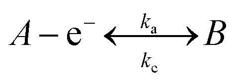 | (1) |
| j = ka[A]0 − kc[B]0 | (2) |
| kc = k0exp((−αF(E − E0f)/RT)) | (3) |
| ka = k0exp((βF(E − E0f)/RT)) | (4) |
In these equations the transfer coefficients α + β = 1, k0 is the standard electrochemical rate constant, E is the electrode potential, E0f is the formal potential and [ ]0 is the surface concentration of the analyte. Fig. 1 depicts an electrochemical simulation for varying k0 values which shows that as the electrochemical oxidation of A to B occurs an overpotential results as the value of k0 is reduced from 10 to 10−10 cm s−1. This change in voltammetric response is exactly that hoped for in the literature where a slow electrode material is utilised with an electrocatalytic material to quantitatively change the voltammetric profile from an irreversible response (∼10−10 cm s−1; Fig. 1) to that of a fast reversible case (∼10 cm s−1; Fig. 1). However, what is most important in electroanalysis is the magnitude of the electrochemical response and one can readily observe from inspection of Fig. 1 that while going from an irreversible process to that of a reversible process there is a change in the magnitude of the peak current (analytical signal), it is not a dramatic change. Indeed, the Randles–Śevčík equation for reversible and irreversible process under diffusion control are respectively given by:
| IAnalytical signalP, Reversible = 2.69 × 10⁵n3/2AC1/2ν1/2D1/2 | (5) |
| IAnalytical SignalP, Irreversible = 2.99 × 10⁵β1/2nAC1/2ν1/2D1/2 | (6) |
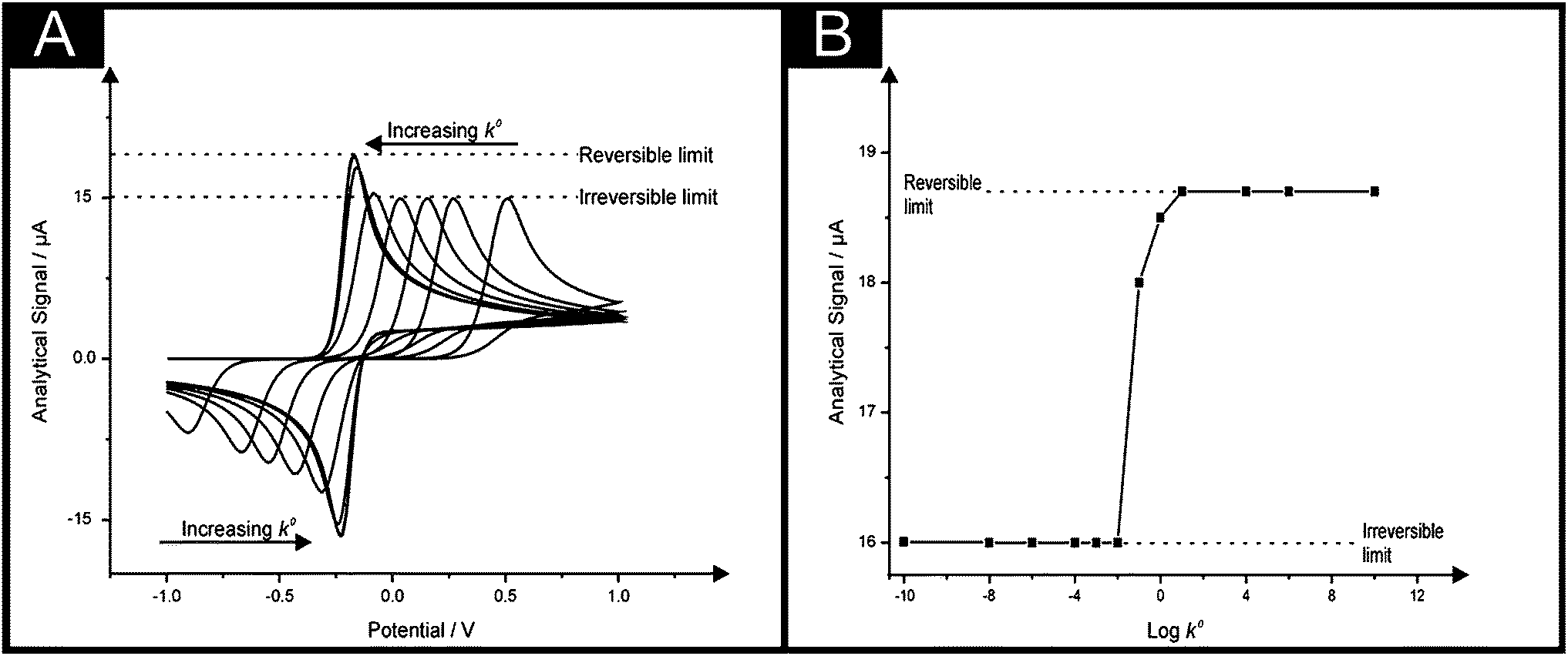 | ||
| Fig. 1 The electrochemical simulation (A) for varying k0 values. E0/V = 0.2; ∝ = β = 0.5; k0/cm s−1 varied between 10 and 1 × 10⁻¹⁰; DA = DB: 1 × 10⁻⁶ cm2 s−1; T = 298.2 K; Electrode area = 0.0707 cm2 (planar geometry); Concentration (A): 1 mM; Scan rate: 1 V s−1. Part (B) shows the analysis of the simulated voltammetric peak current (analytical signal, from A) plotted against log10k0. Program: Digisim®. | ||
Thus, assuming a simple one electron reduction (n = 1) the ratio of the two variants of the Randles–Śevčík equation are:
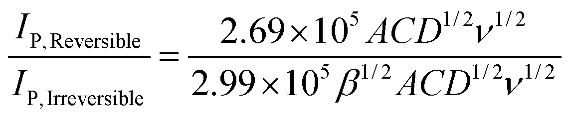 | (7) |
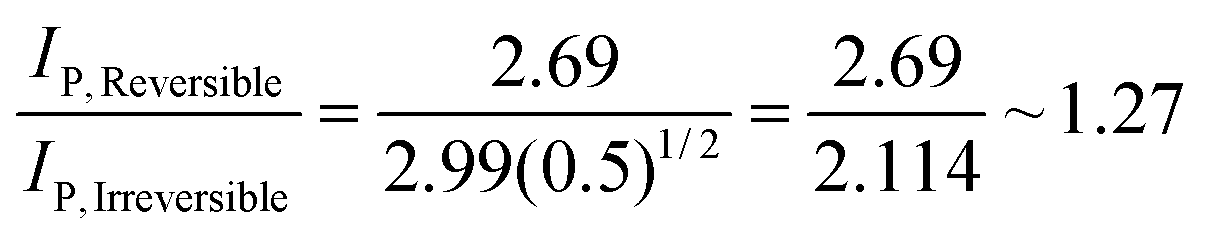 | (8) |
Consequently the analytical signal observed in Fig. 1 changes only by a factor of 1.27, hardly a ground breaking change. This considers the extreme case, in reality one might go from an irreversible to a quasi-reversible process, which is given by:
| IAnalytical signalP, Quasi-reversible = 2.65 × 10⁵n3/2ACD1/2ν1/2 | (9) |
Consequently another approach to dramatically improve the magnitude of the voltammetric peak height is to increase the surface area of the electrode. From inspection of eqn (5) and (6) one can readily observe that if everything is kept constant, with only the electrode area changing, the corresponding voltammetric peak height will increase proportionally. This physical change in geometry is observed in electroanalysis by an increase in the voltammetric peak height which allows lower concentrations of the target analyte to be measured exhibiting a lower limit of detection compared to the unmodified electrode and consequently an increase in the gradient of a plot of peak current (analytical signal) against concentration is observed.
Commonly in the literature, researchers modify their electrodes with carbon nanotubes to increase the surface area. Note that multiple loadings are made onto an electrode surface in order to increase the electrode area as much as possible which is physically limited by how much material can be reproducibly immobilised. Researchers have done this and observed an “electrocatalytic” response, again for clarity, that is a decrease in the overpotential and an increase in the peak current/analytical signal. In essence a carbon nanotube film has been created which is porous in nature and researchers have made the mistake of claiming that carbon nanotubes themselves are “electrocatalytic” giving rise to the observed improvements when actually it is due to the porous nature of the carbon nanotube layer which gives rise to ‘thin-layer’ type voltammetric profiles since the electroactive species gets trapped within the porous carbon nanotube structure.10,11
Since the analytical reproducibility of carbon nanotube modified sensors is questionable and hard to control, the move toward screen-printed carbon nanotube electrodes has resulted.12–14
If we keep everything constant, the working electrode geometry, with no recourse to the implementation of stirring, no modification with any “electrocatalytic” materials, the question still remains, how can one improve the electroanalytical signal in a reproducible, yet simple manner?
In this paper we demonstrate for the first time the back-to-back concept that utilises the “dead” space of screen-printed electrodes. Fig. 2 shows the concept where screen-printed band electrodes (see Fig. 2A: working electrode dimensions of 100 μm with and 20 mm length) are fabricated “back-to-back” and are termed B2-SPEs. Fig. 2B depicts this experimental approach which is simple, cost effective and easy to implement. This methodology utilises the “dead-space” associated with planar screen-printed electrodes and requires no change to the way the electrode is connected/electrically wired to the potentiostat; the two working electrodes are screen-printed on both the front and back of the plastic substrate and are connected in unison (with both the counter and reference electrode connected in the same manner). Such an approach is so simple that we believe that it has not ever been reported before and is only possible using screen-printed electrodes and other electrodes that are able to be fabricated onto a planar surface. The electrochemical and electroanalytical efficiency of the approach is explored with the outer-sphere redox probe hexaammine-ruthenium(III) chloride and the model analytes NADH and nitrite. Due to the electrodes geometric size, such a sensor configuration is particularly useful for small sample volumes. Additionally, if sample volume is not a limitation, through intelligent design, a double “back-to-back” electrode configuration comprising four electrodes can be realised, as shown in Fig. 2C.
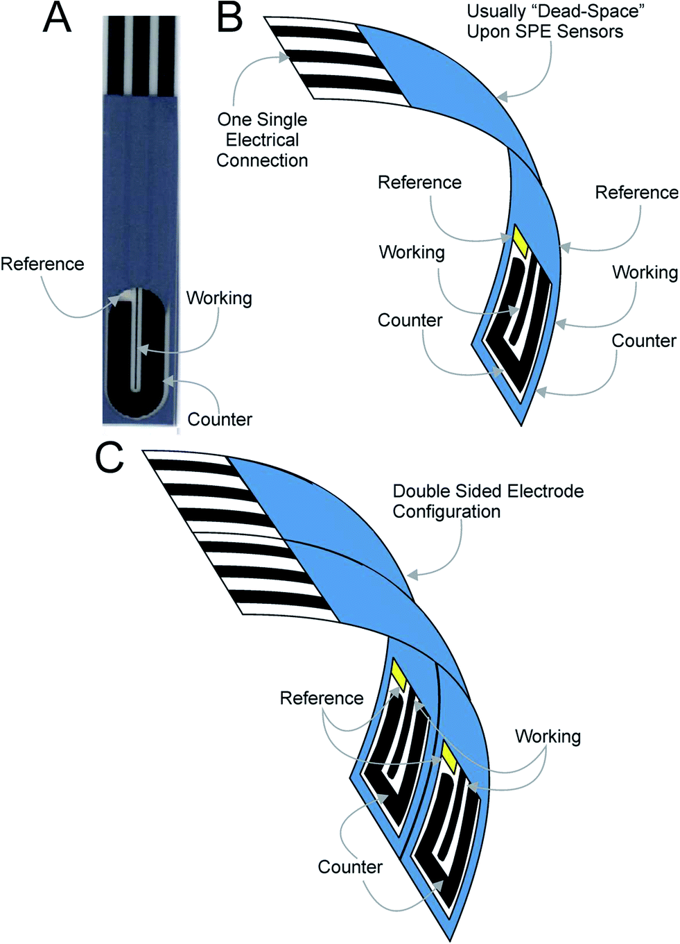 | ||
| Fig. 2 (A) An optical image of a typical B2-SPE showing the electrode layout of the working, counter and reference electrodes. (B) and (C) depict conceptual images introducing the B2-SPE and B4-SPEs respectively where in this configuration the electrodes are fabricated back-to-back and share a common set of electrical connections to the potentiostat. | ||
2. Experimental
All chemicals used were of analytical grade and were used as received without any further purification and were obtained from Sigma-Aldrich. All solutions were prepared with deionised water of resistivity not less than 18.2 MΩ cm. Voltammetric measurements were carried out using a Palmsens (Palm Instruments BV, The Netherlands) potentiostat.All measurements were conducted using a screen-printed three electrode configuration consisting of a carbon–graphite geometric working electrode, carbon–graphite counter electrode and Ag/AgCl reference. Screen-printed graphite band electrodes were fabricated in-house with appropriate stencil designs using a microDEK 1760RS screen-printing machine (DEK, Weymouth, UK). A carbon–graphite ink formulation previously utilised (carbon conductive ink, Gwent Electronic Materials Ltd, UK) was first screen-printed onto a polyester flexible film (Autostat, 250 μm thickness). This layer was cured in a fan oven at 60 degrees for 30 minutes. This layer defines the graphite band electrode which, as shown in Fig. 2A, tailors off onto a larger size graphite pad to enable ease of connection to the potentiostat. Next a silver/silver chloride reference electrode was included by screen printing Ag/AgCl paste (40:60 silver/silver chloride ink, Gwent Electronic Materials Ltd, UK) onto the plastic substrate. Last a dielectric paste ink (Gwent Electronic Materials Ltd, UK) was printed to cover the connection and define the carbon–graphite working electrode. After curing at 60 degrees for 30 minutes the screen-printed electrode is ready to use.
For the fabrication of the three sensors different stencils were utilised designed to produce the desired working electrode geometries. The stencil utilised for the fabrication of the co-planar screen-printed macro electrode (ST-SPE) provided a working electrode geometry of 3 mm in diameter, similarly the microdisc screen-printed electrode (MD-SPE) provided a working electrode geometry of 500 μm in diameter, while that utilised for the microband screen-printed electrode (B-SPE) produced a working electrode area of 100 μm in width and 20 mm in length. These electrodes have been reported and characterised in our other work.15–18 In the case of the ultra-microband screen-printed electrode (μB-SPE) the working electrode fabricated was of the dimensions of 100 μm in width and 2 mm in length. The reproducibility of the fabricated batches of electrodes were explored through comparison of cyclic voltammetric responses using 1 mM hexaammine-ruthenium(III) chloride/0.1 M KCl. Analysis of the voltammetric data revealed the % relative standard deviation to correspond to no greater than 0.94% (±0.03) (N = 20) for electrodes fabricated via screen-printing and using the above experimental parameters which highlights the reproducibility of the fabricated electrodes and their use in electroanalysis. Note that when the electrodes are produced back-to-back, a superscript “2” is introduced, such that in the case of the microband electrode (B-SPE) being fabricated back to back, it is termed B2-SPE. Further to this, when the electrodes are fabricated in a four electrode configuration (superscript “4”) the sensor comprises two back-to-back sensors side-by-side (viz.Fig. 2C). DropSens dual electrodes were commercially obtained from the UK distributor for DropSens, (Spain).19 These electrodes were determined to consist of two working electrodes elliptical in geometry exhibiting major and minor axes of 3464.03 and 1845.32 μm respectively separated by a centre to centre distance of 1025.18 μm (minimum).
3. Results and discussion
3.1 Introducing the “back-to-back” electrode configuration
In order to first explore the potentially useful nature of the back-to-back electrode configuration, a crude electrochemical cell was first constructed. The cell consisted of two individual screen-printed electrodes physically positioned “back-to-back” which constituted the working electrodes and counter electrodes (one for each working electrode which are screen-printed alongside each of the working electrodes). To complete the cell an external saturated calomel electrode (SCE) was connected which was shared between the working and counter electrodes. In the case of the two working and counter electrodes a single connection was utilised, thus connecting the respective electrodes. It was quickly noted that in such an electrochemical configuration the position of the SCE was critical in dictating the observed voltammetric response. Cyclic voltammetric responses obtained at different electrode configurations relating to the position of the reference electrode in relation to the working electrode(s) revealed the critical role played by the reference electrode with regard to the observed response. It was determined that if the reference electrode is positioned to be facing only one of the two working electrodes comprising the back-to-back configuration then the observed voltammetric response (reduction peak height) shows a minimal improvement (×1.04, using the electrochemical redox probe hexaammine-ruthenium(III) chloride) over that offered at a single co-planar graphite screen-printed macro electrode (denoted throughout as ST-SPE). Importantly however, when two SCE reference electrodes (sharing a common connection) are positioned with each facing the two working electrodes comprising the back-to-back configuration an improvement of ×1.91 (with respect to the reduction peak height) is noted in comparison to the ST-SPE. Such observations are in agreement with previous work by Costa-Garcia et al.20 who reported that in sensor design, the distance between electrodes comprising the sensor is critical.As has been highlighted within the introduction, screen-printed sensors have, in recent times, exhibited the potential for the development of electrochemical devices intended for analytical applications which can truly be implemented in to the field. Undoubtedly the most utilised configuration is the co-planar disc-shaped electrode (extensively reported upon within the literature16,17,21–25) typically consisting of a 3 mm diameter working electrode, the response of which we first explore.
First a back-to-back co-planar graphite (3 mm diameter) screen-printed macro electrode (denoted throughout as ST2-SPE) was fabricated as described in the Experimental section to produce, for the first time, a screen-printed sensor comprising two complete electrochemical sensing devices on a single substrate and due to the configuration, each electrode experiences independent, non-overlapping diffusional zones. Note that if these electrodes were simply put next to each other on the same side without consideration of the distance between these electrodes, the electroanalytical response would not be optimum since diffusional interaction between the two electrodes will occur (see later for a more detailed discussion). The ST2-SPE was compared and contrasted with a single co-planar graphite screen-printed macro electrode using the well characterised redox probe hexaammine-ruthenium(III) chloride. Fig. 3 show typical cyclic voltammograms obtained in 1 mM hexaammine-ruthenium(III) chloride where in comparison of a single screen-printed macro electrode with that of the double sided screen-printed macro electrode, an improvement in the magnitude of the voltammetric current (analytical signal) is observed. It is found that an average improvement of 1.82 is observed in the voltammetric response over the applied voltammetric scan rate (5–200 mV s−1); at slower applied scan rates the observed improvement is close to 2 but at the faster scan rates this deviates. As predicted by eqn (5), since one is effectively doubling the size of the working electrode area, the peak current/analytical signal should simply double in magnitude.
 | ||
| Fig. 3 Cyclic voltammograms recorded in 1 mM hexaammine-ruthenium(III) chloride/0.1 M KCl at scan rates of 5 mV s−1 (A) and 100 mV s−1 (B) using a single ST-SPE (dotted line) and ST2-SPE (solid line). | ||
Next attention was turned to exploring the electrochemical response of a 500 μm (diameter) microdisc-SPE (MD-SPE) as evaluated using the redox probe hexaammine-ruthenium(III) chloride. As shown in ESI Fig. 1,† improvements in the analytical signal (peak current) are observed to result in the use of the back-to-back configuration where again over the applied scan rates, deviation from 2 is observed as the scan rate is increased. Next, the electrode configuration of a 100 μm microband-SPE (B-SPE) was explored and the voltammetric responses are again shown in ESI Fig. 2.† Note that in the comparison of Fig. 3, 4 and 5, the quantitative change in the voltammetric shape is as expected in going from that of a macroelectrode to a microband where the mass-transport characteristics change due to the physical geometric changes. In the case of the B2-SPE configuration, an improvement of 2.01× in the magnitude of the voltammetric response across scan rate range studied (5–200 mV s−1) was observed.
In the implementation of the back-to-back configuration as introduced above, one is effectively doubling the electrode area, and as such, it can be readily observed from eqn (5) that this results in a doubling in the magnitude of the peak current (Ip). The reason that this doesn't hold true over the scan rate range applied for the ST2-SPE and MD2-SPE is that a capacitive (background) charging current, IC, is generated which is directly proportional to the applied voltammetric scan rate, as given by:
| IC/A = (1/A)(dQ/dt) = C′(dE/dt) = C′ν | (10) |
Another approach that could potentially be used is a large macroelectrode, that way, the electrode area is increased and hence as predicted by eqn (5), the peak current will increase proportionally. Therefore, if we were to use an electrode of 10 times the area, it should give 10 times the response. Such improvement would be highly significant, if the background noise were to remain at its original value; we term noise as non-faradaic processes which encompass capacitance as well as electricity-power noise and electronic amplification and offer various factors and hence it is desirable to minimize such noise. If we increase the electrode area and if the noise was to increase proportionately, the use of a larger surface is questionable. The parameter most useful for analytical comparison is the signal-to-noise ratio. As the electrode surface area increases, the signal-to-noise ratio becomes unfavourable and it becomes harder to differentiate the analytical signal from the background response, hence why electrochemists move from a macro to a micro electrode geometry since the latter yield improvements in the signal-to-noise ratio. As such this likely explains why in the case of the macroelectrode SPEs (ST-SPE for example) that the back-to-back configuration didn't scale by a factor of 2 and that the transition to the microband electrodes did. Additionally the use of a very large electrode would equally not be of use since of the discussions above.
3.2 Introducing the B4-SPE electrode configuration
It is important to point out that a different configuration could potentially be envisaged, that is, placing electrodes next to each other, effectively producing an array of electrodes which are connected in unison. However, a practical consideration is the magnitude of the diffusion layer/zone size, δ, which is a function of the applied voltammetric scan rate, the diffusion coefficient of the electroactive analyte as given by (in 3D):18 | (11) |
 | (12) |
In the above equation ΔE is the potential width of the observed voltammetric signal corresponding from a non-faradaic to faradaic process, the deduction of which is shown in ESI Fig. 4.† In order for the electrode array to work electroanalytically efficiently, diffusional interaction needs to be minimal otherwise the observed analytical response and analytical sensitivity will not be the magnitude it should as predicted by theory. In order to achieve diffusional independence there should be a sufficient physical distance between neighbouring electrodes comprising the array.
To the best of the author's knowledge only one similar configuration currently exists which is marketed commercially19 but rather than have two electrodes on different sides of the substrate, as shown here, this sensor comprises a single reference and counter electrodes servicing two separate elliptical working electrodes which are position on the same side; again the redundant dead-space of the back of the sensor has not been utilised. These elliptical duel working electrodes each boast a working electrode of 4 mm in diameter separated from one another by a distance of 1 mm. Critically in such a configuration the electrodes are working in an array format (connected in unison) which is often unfortunately and incorrectly undertaken with little, or no regard to the interaction of diffusion layers of neighbouring electrodes.26,27 If we consider this dual electrode, for optimal electroanalytical performance, there should be no diffusion layer interaction between neighbouring electrodes such that the diffusion layer, δ, as given by eqn (12) must be less than fgreater, as given by:18
 | (13) |
In reality, one needs to design an electrode that ensures diffusional interaction is maintained at all times which encompasses a wide range of applied voltammetric scan rates, the potential range of the electroactive species and the associated diffusion coefficients of the target analytes under electroanalytical investigation (see equation above (12)). Note that diffusion coefficients are dependent upon electrolyte composition,29 solution viscosity30,31 and temperature28 and in reality, one will encounter such experimental variations that will change the magnitude of the diffusion zones and a duel electrode with a fixed distance might encounter diffusional independence in one scenario but will give rise to diffusional dependence in another, with associated losses in (electro) analytical performances; hence such a fixed electrode format might have limitations.
In order to ensure that diffusional interaction is completely avoided, in all possible scenarios, taking into the considerations above, the distance between electrode will need to be relatively large such that the overall size of the sensor become too large and potentially loses the advantages of screen-printed sensors, such as reduced solution volume, and will generally be too large to be of a practical size; for example the commercial dual electrode requires 500 μL of solution. A much simpler and effective approach is to utilise the double sized electrode configuration and due to the geometric configuration, diffusion layers/zones will never interact.
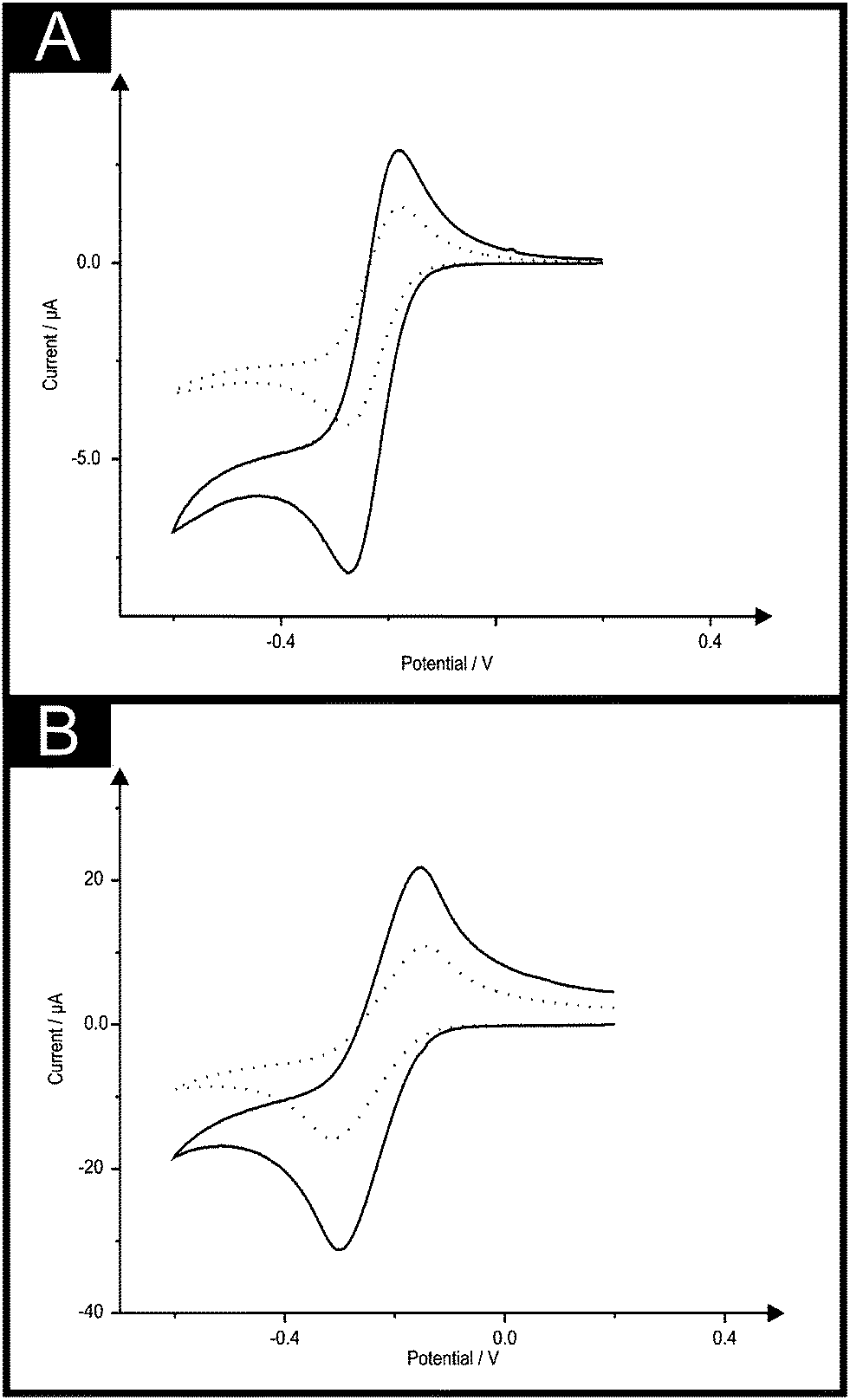
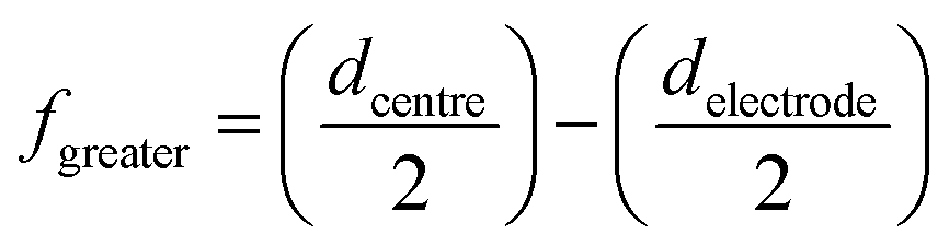
To further explore the potential of such ingenious electrode configurations the behaviour of a back-to-back sensor comprising four electrodes (B4-SPE) was explored. Here a sensor comprising two B-SPEs on each side (viz.Fig. 2C) was implemented for the measurement of the same electrochemical redox probe hexaammine-ruthenium(III) chloride with the observed response being compared with that of a single B-SPE electrode. Fig. 4A & B depict the cyclic voltammetric response obtained at scan rates of 5 and 100 mV s−1 using both the B-SPE and B4-SPE, whereby at both scan rates depicted the response is seen to quadruple upon use of the B4-SPE when compared to B-SPE. Such observations highlight the impressive potential of such configurations which could be of great use in particular applications. Similarly, some applications may present a solution volume which is very limited (low microlitre range) where the utilisation of a small sensor would be necessitated. To ensure the benefits noted at the sensors previously explored were still applicable to a sensor of further reduced size an ultramicroband screen-printed electrode (μB-SPE) (see Experimental section for further details) was employed. Here the cyclic voltammetric response of a single μB-SPE was compared with that of a sensor comprising four ultramicroband screen-printed electrodes configured in a back-to-back configuration (as described above for the B4-SPE) denoted as μB4-SPE using the redox probe hexaammine-ruthenium(III) chloride. Depicted in Fig. 4C & D are the responses obtained at the μB-SPE and μB4-SPE at both 5 and 100 mV s−1, where it is evident that the voltammetric signal is amplified by 3.9 and 4.0 times respectively.
 | ||
| Fig. 4 Cyclic voltammograms recorded in 1 mM hexaammine-ruthenium(III) chloride/0.1 M KCl using a single B-SPE (dotted line) and B4-SPE (solid line) at scan rates of 5 mV s−1 (A) and 100 mV s−1 (B). Also shown are cyclic voltammograms obtained using a single μB-SPE (dotted line) and μB4-SPE (solid line) at scan rates of 5 mV s−1 (C) and 100 mV s−1 (D). | ||
3.3 Exploring the electroanalytical efficiency of the B2-SPE and B4-SPE configurations
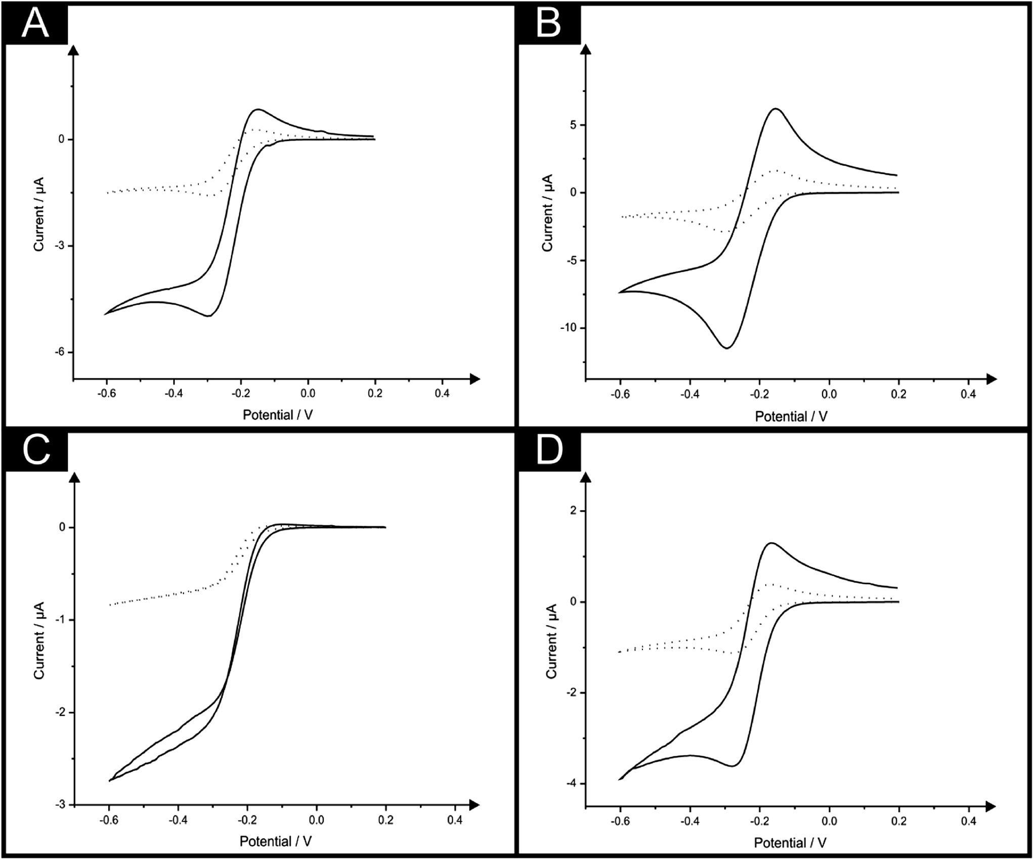
In order to demonstrate the (electro)analytical efficiency of the double printed screen-printed sensors, we turn to the exploring the analytical response of the electrochemical oxidation of NADH due to its use in over 300 + biosensors15,32,33 focusing on the utilisation of the B2-SPE. Fig. 5A shows the electrochemical oxidation of NADH at a B-SPE and B2-SPE where again useful improvements of the peak current are observed through the use of the latter. Fig. 5B shows a calibration plot obtained using a single and B2-SPE (ESI Fig. 5† also demonstrates the responses obtained in the blank phosphate buffer solution at pH 7). It is evident through inspection of Fig. 5 that both the B-SPE and B2-SPE exhibit linear responses over the analytical ranges studied (B-SPE: 2–10 μM, B2-SPE: 1–10 μM) offering limits of detection (3σ) of 1.75 and 0.96 μM for the B-SPE and B2-SPE respectively. What is of prime interest is that the B2-SPE allows a lower concentration to be measured that at the B-SPE show the benefit of using the former over the latter. It is apparent that greater sensitivity is noted at the B2-SPEs (IP/μA = 6.8 × 10⁻³μA/μM + 1.1 × 10⁻² μA; R2 = 0.99; N = 10) over that of a single B-SPE (IP/μA = 3.1 × 10⁻³ μA/μM + 4.8 × 10⁻³ μA; R2 = 0.97; N = 10), which is once more attributed to the novel configuration of the sensor. Note that the analytical sensitivity is doubled through the use of the B2-SPE. When benchmarking this determined limit of detection against other electrochemical reports present within the literature relating to the determination of NADH such a limit of detection is deemed favourable, for example as reported by Marty et al.34 where carbon based screen-printed sensors modified using Medola Blue reporting a limit of detection of 2.5 μM. Ultra-low NADH detection limits (0.16 μM) have also been reported by Zen and co-workers35 using mediator-less screen-printed carbon electrodes, though the exceptionally low detection limits are attributed to the surface reorientation which is said to generate more edge plane arising from a pre-anodization procedure where the screen-printed sensor used was electrochemically oxidised by applying a potential at +2.0 V (vs. Ag/AgCl). A more laborious method reported for the detection of NADH involves the modification of a traditional gold macro electrode with a thin thiol film as described by Behera and Raj,36 where both thiocytasine and mercaptopyrimidine were utilised to form the thiol films obtaining detection limits of 0.5 μM and 2.5 μM respectively.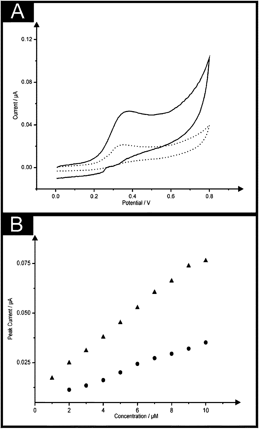 | ||
| Fig. 5 (A) A comparison of cyclic voltammograms obtained in 6 μM NADH in a pH 7 phosphate buffer solution using the B-SPE (dotted line) and B2-SPE (solid line). Scan rate: 50 mV s−1. (B) Overlaid calibration plots for the addition of NADH (1 to 10 μM) into a pH 7 phosphate buffer solution at the B-SPE (circles) and B2-SPE (triangles). | ||
As described above, through the use of the B2-SPE electrode one has effectively doubled the electrode area which has resulted in a double improvement of the analytical signal (peak current, IP). Note that this produces a highly reproducible improvement in the peak current (analytical signal) which is not easily obtainable from using nanomaterials to increase the electrode area. From inspection of eqn (5)§ one can readily see that another approach to double the analytical signal would be to increase the scan rate, since IP is proportional to v1/2.
We next consider the only other viable other approach to improve the electroanalytical sensitivity is to change the voltammetric scan rate and in order to achieve the doubling of the peak current, a scan rate of 200 mV s−1 needs to be applied as governed by equation with everything else being equal (same solution composition and so on). It would appear that this is easily achievable and could potentially be easier than fabricating the double sided SPEs. This is further explored in Fig. 6 where the electroanalytical response of NADH at the scan rate of 50 mV s−1 using the B-SPE and B2-SPE as depicted in Fig. 5, however in this instance, comparison is also made with that obtained at a single B-SPE at a faster scan rate of 200 mV s−1. What is evident is that the lowest concentration value is not distinguishable from the blank (i.e. the faradaic response is very close to the non-faradaic response) and the concentration point 1 micro-molar is absent on all but the B2-SPE configuration. Again this is related to the generated capacitive charging current which appears on the voltammetric signal as a non-faradaic process and the background current increases which masks signals observed at low analyte concentrations.
 | ||
| Fig. 6 Calibration plots resulting from the addition of NADH (1 to 10 μM) into a pH 7 phosphate buffer solution using the B-SPE (circles) and B2-SPE (squares) at a scan rate of 50 mV s−1 and B-SPE (triangles) at a scan rate of 200 mV s−1. | ||
Last, one other potentially viable method to assist in the development of this area is that proposed by Lan et al.37 However, if we consider the work of Lan et al. who reported a porous screen-printed electrode (SPE), in comparison to a non-porous SPE we find that the current improvement towards potassium ferrocyanide gives, at best, an increase of 1.7 with the former reported to exhibit a %RSD of 6.5%. Further work by these authors explored the case of the sensing of hydrogen peroxide. However if we analyse the data from their paper we find that the porous vs. the non-porous exhibits a factor of 2.8 increase. Clearly the discrepancy between 1.7 and 2.8 indicates the potentially non-reproducible nature of the fabrication approach;37 if this could be overcome with the use of the back-to-back approach even more significant improvements in the analytical response would be observed.
3.4 Applying the B2-SPE and B4-SPE for the electroanalytical sensing of nitrite
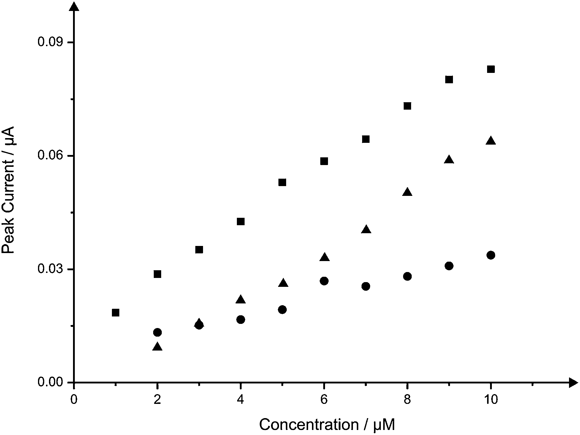
Nitrite was next explored since its electrochemistry is well known and characterised on graphite based electrodes.15,38–40 Nitrite is widely involved in environmental chemistry and public health, so the important roles played by nitrite in these areas were recognized long ago.41,42 Although naturally-occurring concentrations of nitrites are usually of no significance to health, wastes from fertilizers and the intentional addition of nitrites for corrosion control are potential sources of nitrite contamination.43 Nitrite is reported to be a human health-hazard chemical the excess of which may cause poisoning and its derivatives are also major components in low-level radioactive waste solution.44,45 The excess uptake of nitrite could cause gastric cancer46 and it is therefore necessary to develop a reliable and sensitive sensor to detect nitrite in food, drinking water and environmental samples. Fig. 7 depicts the voltammetric profiles resulting from the additions (10 to 100 μM) of nitrite into a pH 7 phosphate buffer solution using both the B-SPE and B2-SPE. Inspection of Fig. 7 reveals as expected, and in similar fashion to the voltammetry obtained for NADH, linearity over the entire analytical range of nitrite at both the B-SPE (IP/μA = 1.4 × 10⁻² μA/μM + 6.4 × 10⁻² μA; R2 = 0.99; N = 10) and B2-SPE (IP/μA = 3.0 × 10⁻² μA/μM + 9.4 × 10⁻² μA; R2 = 0.99; N = 10); no attempt to remove outliers in the linear regression has been made. Note that the back-to-back configuration results in a clear improvement of a factor of 2, that is, the (electro) analytical sensitivity has been doubled. Also explored for the case of nitrite was the potential use of the B4-SPE for electroanalytical applications. Nitrite was measured over the same concentration range using a B4-SPE, providing a linear response over the entire range studied (IP/μA = 5.5 × 10⁻² μA/μM + 2.3 × 10⁻¹ μA; R2 = 0.99; N = 10) whilst maintaining an improvement of at least 4 times with regard to the signal magnitude over that offered at the B-SPE. Additionally the limits of detection (3σ) for the determination of nitrite at the B-SPE, B2-SPE and B4-SPE were calculated to be 5.64, 1.02 and 0.54 μM respectively. In addition to showing impressive analytical improvements over the B-SPE, consultation of the literature reveals that this simple, yet novel, configuration exhibited by both the B2-SPE and B4-SPE is also competitive with current literature for the electroanalytical determination of nitrite; see ref. 18 for a summary of electrochemical protocols reported for the determination of nitrite.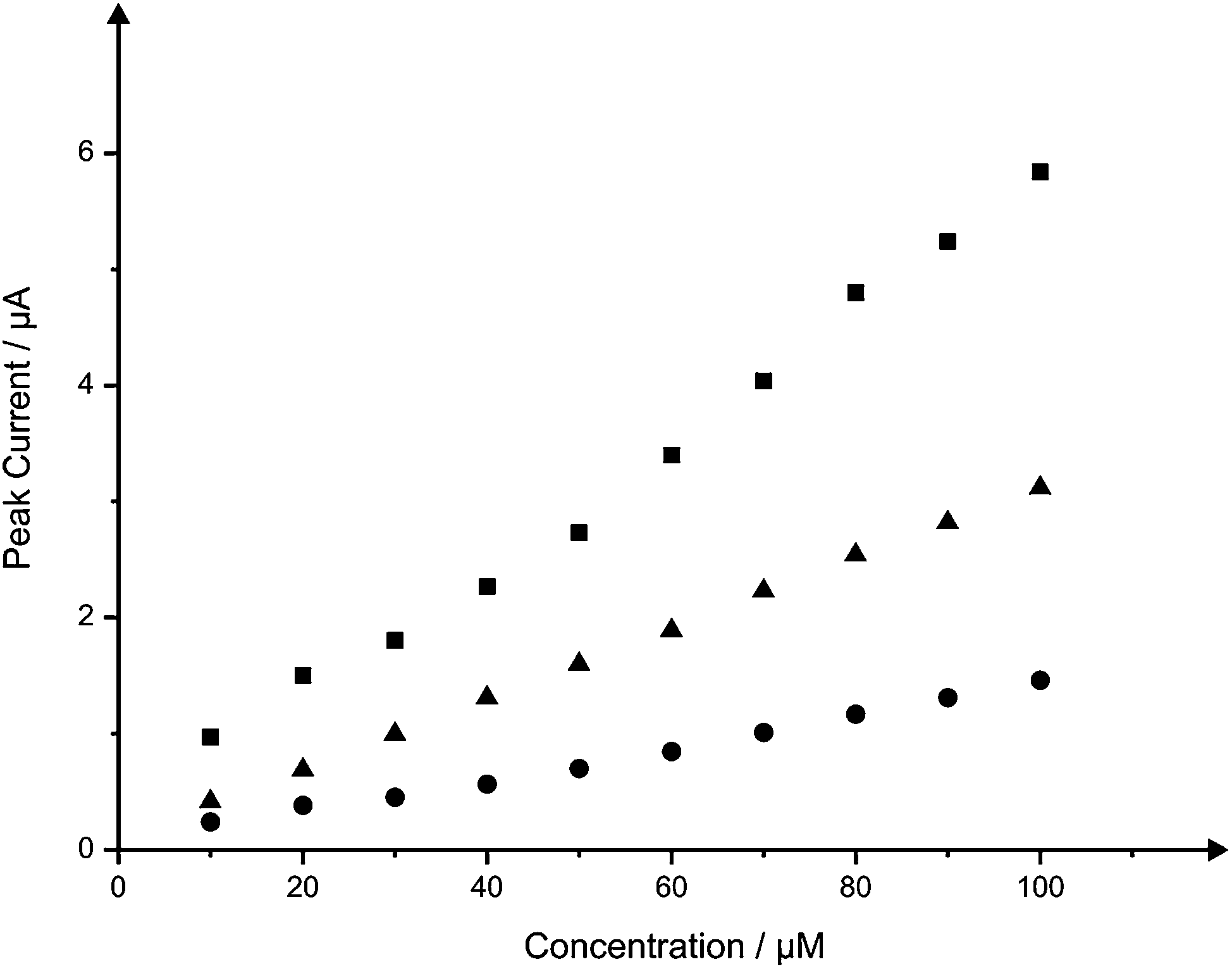 | ||
| Fig. 7 Overlaid calibration plots for the addition of nitrite (10 to 100 μM) into a pH 7 phosphate buffer solution at the B-SPE (circles) and B2-SPE (triangles) and B4-SPE (squares). Cyclic voltammograms corresponding to the response obtained at the three electrode configurations at a concentration of 60 μM nitrite are shown in ESI Fig. 6.† | ||
Last, Table 1 offers a comprehensive breakdown comprising the relevant information obtained when exploring the analytical performance of the B, B2 and B4-SPEs configurations towards the sensing of NADH and nitrite. As mentioned in the introduction, researchers will often substantially increase their working electrode areas, such as through modification with nanomaterials, in order to increase the analytical signal (voltammetric peak height); in comparison of the unmodified electrode with that of the modified electrode, where the latter has a larger surface area over the former, a substantial improvement in magnitude of the voltammetric peak height will be observed with an associated increase in the sensitivity. This approach is common in the literature, yet if one divided the modified electrode with the new area, one will see that there is no difference in the observed sensitivity, that is, the gradient of a plot of peak height/analytical signal against concentration. The same is true from inspection of Table 1 where in both cases for nitrite and NADH sensing, the observed sensitivity is increase by a factor of 2 and 4 when using the B2-SPE and B4-SPE over that of the B-SPE. Of course if we normalise for the increase in electrode area, the sensitivity, in the form of (μA cm−2)/μM is effectively constant between the electrodes. What is of interest is that the limits of detection (3σ) are substantially reduced in using both the B2 and B4 configurations and is still the case when accounted for the change in the electrode area. The detection limit is defined as the minimum value of the signal from the target analyte being measured that is significantly different from the blank signal, which is defined mathematically corresponding to ksb/m, where k is a numerical factor chosen in accordance with the confidence level (usually 3, known as 3-sigma), sb is the standard dictation of the y-residual from the line of best fit and m is the analytical sensitivity. From inspection of Table 1, it can be clearly seen that the analytical sensitivity is increased by a factor of 2 and 4 in the case of the B2-SPE and B4-SPE respectively. The difference between the analyte signal and the background is substantially increased giving rise to the observed limits of detection; this can easily be observed with respect to the This is observed experimentally in Fig. 5 for example, where the B2-SPE allows a lower concentration to be measured that at the B-SPE. Thus inputting the increased analytical sensitivities (that is the gradient from a plot of peak current against concentration with the units of AM−1) into the limit of detection equation one can readily observe that the B2-SPE and B4-SPE give rise to improved limits of detection over that of the B-SPE.
| Analyte | Electrode | Sensitivity μA μM−1 (±error) | Normalised sensitivity (μA cm−2)/μM | LOD (3σ)/μM |
|---|---|---|---|---|
| NADH | B-SPE | 3.14 × 10⁻³ (±0.26 × 10⁻³) | 7.58 × 10⁻¹ | 1.75 |
| B2-SPE | 6.82 × 10⁻³ (±0.29 × 10⁻³) | 6.89 × 10⁻¹ | 0.96 | |
| Nitrite | B-SPE | 1.36 × 10⁻² (±0.09 × 10⁻²) | 1.3 × 10⁻¹ | 5.64 |
| B2-SPE | 3.03 × 10⁻² (±0.11 × 10⁻²) | 1.82 × 10⁻¹ | 1.02 | |
| B4-SPE | 5.51 × 10⁻² (±0.12 × 10⁻²) | 6.82 × 10⁻¹ | 0.54 |
4. Conclusions
We have shown proof-of-concept for a simple and facile approach to improving the analytical performance of screen-printed electrochemical based sensors in terms of doubling and quadrupling the analytical sensitivity as well as reducing the limit of detection which is achieved through printing onto both sides of the electrode substrate where these are electrically connected in unison (see Fig. 2). This approach utilises for the first time the “dead space” on the back of screen-printed sensors which is overlooked and has never been reported in the literature before. The approach allows two electrodes to be connected in unison without diffusional interaction since the electrode are back-to-back rather than next to each other on the same planar surface where the latter, if not sufficiently separately would diffusionally interact with each other reduce the electroanalytical performance. Through the use of screen-printed double sided electrodes, mass producible sensors which exhibit double the sensitivity are realised for the first time and avoids the need for modification of electrode surfaces with nanomaterials¶ which can result in a poor reproducibility. We have also demonstrated that through intelligent design that a ×4 improvement can also be readily achieved. The approach is generic and potentially any screen-printed electrode configuration can be realised bands,15,32 discs,18 recessed electrode configurations38 porous, macro and nano modified11,47 configurations etc.; other variants are currently being explored.References
- G. G. Wildgoose, C. E. Banks, H. C. Leventis and R. G. Compton, Microchim. Acta, 2006, 152, 187 CrossRef CAS.
- R. R. Moor, C. E. Banks and R. G. Compton, Anal. Chem., 2004, 76, 2677 CrossRef PubMed.
- J. Wang, Electroanalysis, 2004, 17, 7 CrossRef PubMed.
- S. Griese, D. K. Kampouris, R. O. Kadara and C. E. Banks, Electroanalysis, 2008, 20, 1507 CrossRef CAS PubMed.
- Y. Shao, J. Wang, H. Wu, J. Liu, I. A. Aksay and Y. Lin, Electroanalysis, 2010, 22, 1027 CrossRef CAS PubMed.
- D. A. C. Brownson and C. E. Banks, Analyst, 2010, 135, 2768 RSC.
- D. A. C. Brownson, D. K. Kampouris and C. E. Banks, Chem. Soc. Rev., 2012, 41, 6944 RSC.
- IUPAC Gold Book, http://goldbook.iupac.org/S05606.html, accessed March 02014.
- H. L. Pardue, Clin. Chem., 1997, 43, 1831 CAS.
- I. Streeter, G. G. Wildgoose, L. D. Shao and R. G. Compton, Sens. Actuators, B, 2008, 133, 462 CrossRef CAS PubMed.
- E. P. Randviir, D. A. C. Brownson, J. P. Metters, R. O. Kadara and C. E. Banks, Phys. Chem. Chem. Phys., 2014, 16, 4598 RSC.
- J. P. Metters, M. Gomez-Mingot, J. Iniesta, R. O. Kadara and C. E. Banks, Sens. Actuators, B, 2013, 177, 1043 CrossRef CAS PubMed.
- E. P. Randviir, J. P. Metters, J. Stainton and C. E. Banks, Analyst, 2013, 138, 2970 RSC.
- P. Fanjul-Bolado, P. Queipo, P. J. Lamas-Ardisana and A. Costa-Garcia, Talanta, 2007, 74, 427 CrossRef CAS PubMed.
- J. P. Metters, R. O. Kadara and C. E. Banks, Sens. Actuators, B, 2012, 169, 136 CrossRef CAS PubMed.
- A. V. Kolliopoulos, J. P. Metters and C. E. Banks, Anal. Methods, 2013, 5, 851 RSC.
- A. V. Kolliopoulos, J. P. Metters and C. E. Banks, Anal. Methods, 2013, 5, 3490 RSC.
- F. Tan, J. P. Metters and C. E. Banks, Sens. Actuators, B, 2013, 181, 454 CrossRef CAS PubMed.
- DropSens, http://www.dropsens.com/en/pdfs_productos/new_brochures/c1110.pdf, Accessed March 2014.
- A. M. Pernia, M. J. Prieto, I. C. Orille, J. A. Martin-Ramos and A. Costa-Garcia, IEEE Trans. Instrum. Meas., 2009, 58, 2181 CrossRef.
- R. O. Kadara, N. Jenkinson and C. E. Banks, Electrochem. Commun., 2009, 11, 1377 CrossRef CAS PubMed.
- V. Ostatna, H. Cernocka, K. Kurzatkowska and E. Palecek, Anal. Chim. Acta, 2012, 735, 31 CrossRef CAS PubMed.
- T.-H. Wang, G.-H. Hui and S.-P. Deng, Biosens. Bioelectron., 2010, 26, 929 CrossRef CAS PubMed.
- L. Civit, H. M. Nassef, A. Fragoso and C. K. O'Sillivan, J. Agric. Food Chem., 2008, 56, 10452 CrossRef CAS PubMed.
- G. Martinez-Paredes, M. B. Gonzalez-Garcia and A. Costa-Garcia, Electroanalysis, 2009, 21, 379 CrossRef CAS PubMed.
- T. J. Davies, S. Ward-Jones, C. E. Banks, J. del Campo, R. Mas, F. X. Munoz and R. G. Compton, J. Electroanal. Chem., 2005, 585, 51 CrossRef CAS PubMed.
- A. O. Simm, C. E. Banks, S. Ward-Jones, T. J. Davies, N. S. Lawrence, T. G. J. Jones, L. Jiang and R. G. Compton, Analyst, 2005, 130, 1303 RSC.
- Y. Wang, J. G. Limon-Petersen and R. G. Compton, J. Electroanal. Chem., 2011, 652, 13 CrossRef CAS PubMed.
- V. M. M. Lobo, A. C. F. Ribeiro and S. G. C. S. Andrade, Berichte der Bunsengesellschaft für physikalische Chemie, 1995, 99, 713 CrossRef CAS PubMed.
- C. R. Wilke and P. Chang, AIChE J., 1995, 1, 264 CrossRef PubMed.
- W. Hayduk and H. Laudie, AIChE J., 1974, 20, 611 CrossRef CAS PubMed.
- J. P. Metters, R. O. Kadara and C. E. Banks, Analyst, 2013, 138, 2516 RSC.
- D. A. C. Brownson, J. P. Metters, D. K. Kampouris and C. E. Banks, Electroanalysis, 2011, 23, 894 CrossRef CAS PubMed.
- A. Vasilescu, S. Andreescu, C. Bala, S. C. Litescu, T. Noguer and J.-L. Marty, Biosens. Bioelectron., 2003, 18, 781 CrossRef CAS.
- K. S. Prasad, J.-C. Chen, C. Ay and J.-M. Zen, Sens. Actuators, B, 2007, 123, 715 CrossRef CAS PubMed.
- C. R. Raj and S. Behera, Biosens. Bioelectron., 2005, 21, 949 CrossRef CAS PubMed.
- X. Niu, C. Chen, H. Zhao, J. Tang, Y. Li and M. Lan, Electrochem. Commun., 2012, 22, 170 CrossRef CAS PubMed.
- J. P. Metters, F. Tan, R. O. Kadara and C. E. Banks, Anal. Methods, 2012, 4, 3140 RSC.
- J. P. Metters, S. M. Houssein, D. K. Kampouris and C. E. Banks, Anal. Methods, 2013, 5, 103 RSC.
- B. R. Kozub, N. V. Rees and R. G. Compton, Sens. Actuators, B, 2010, 143, 539 CrossRef CAS PubMed.
- T. R. Camp, Water and its impurities, Reinhold Publishing, New York, 1963 Search PubMed.
- D. E. Metzler, Biochemistry: The chemical reactions of living cells, Academic, New York, 1977 Search PubMed.
- N. Spataru, T. N. Rao, D. A. Tryk and A. Fujishima, J. Electrochem. Soc., 2001, 148, E112 CrossRef CAS PubMed.
- Drinking Water Standards 1962, US Department of Health, Education and Welfare, Public Health Service, Washing DC, 1988 Search PubMed.
- J. M. Concon, Food toxicology: Principles and concepts, Part A, Marcel Dekker, New York, 1988 Search PubMed.
- W. Lijinsky and S. S. Epstein, Nature, 1970, 225, 21 CrossRef CAS.
- C. E. Foster, J. Pillay, J. P. Metters and C. E. Banks, Electroanalysis, 2014 Search PubMed , in Press.
Footnotes |
| † Electronic supplementary information (ESI) available. See E-mail: DOI: 10.1039/c4an01501k |
| ‡ Note that we define sensitivity as the slope of a calibration plot, as defined by IUPAC.8,9 |
| § Note that in this case of a 100 micron diameter microband, it is a pseudo-microband and its departure from that of a macroelectrode means that its mass transport characteristics involve not only the contribution from convergent diffusion (as would solely be the case for a true microelectrode) but also linear diffusion since it is pseudo in nature. Since we have found that the dominant form of mass transport is linear diffusion for our microband due to its physical size, the scan rate (ν) in eqn (5) is readily substituted by wl where w is the width of the microband and l is its corresponding length. As such our argument is valid for our pseudo-microband electrode. |
| ¶ Note that this refers to drop casting carbon nanotubes, for instance, onto a supporting electrode substrate. We have recently shown that the reproducibility of this can be overcome through the use of screen-printed carbon nanotube electrode (see for example J. P. Metters, M. Gomez-Mingot, J. Iniesta, R. O. Kadara and C. E. Banks, Sens. Actuators, B, 177, 1043). Such a configuration could be used “back to back” as reported here. |
| This journal is © The Royal Society of Chemistry 2014 |