
 Open Access Article
 This Open Access Article is licensed under a Creative Commons Attribution-Non Commercial 3.0 Unported Licence
Morphology-controlled green synthesis of tellurium nanostructures and applications of Te/MXene hybrid structures†
Mengchen
Xu‡
a,
Jinshu
Li‡
b,
Qingshan
Yang
b,
Lu
Jiang
a,
Jiaqi
He
 c,
Dawei
He
*a,
Yongsheng
Wang
*a and
Yajie
Yang
*a
c,
Dawei
He
*a,
Yongsheng
Wang
*a and
Yajie
Yang
*a
aKey Laboratory of Luminescence and Optical Information, Ministry of Education, Institute of Optoelectronic Technology, Beijing Jiaotong University, Beijing 100044, China. E-mail: dwhe@bjtu.edu.cn; yshwang@bjtu.edu.cn; yangyj@bjtu.edu.cn
bSKKU Advanced Institute of Nanotechnology (SAINT), Sungkyunkwan University, Suwon 16419, South Korea
cCollege of Mathematics and Physics, Beijing University of Chemical Technology, Beijing 100029, China
First published on 17th October 2023
Abstract
Tellurium (Te), a striking elemental nanomaterial, demonstrated anisotropic physical properties owing to its unique chiral-chain van der Waals structure. Here, morphology-controlled Te nanostructures are synthesized by a viable and eco-friendly solution process, realizing the formation of high-quality two-dimensional (2D) tellurene and one-dimensional (1D) Te nanostructures with controlled morphologies, including nanotubes, nanowires, and nanocables. A reasonable growth mechanism was derived to explain the morphology transformation. Moreover, the two-dimensional material MXene (Ti3C2Tx) was introduced to fabricate transparent conductive electrodes based on Te/MXene hybrid structures, in which low sheet resistance (156 Ω sq−1) and high transmittance (70%) were obtained.
Introduction
Recently, Te nanostructures have attracted considerable attention due to their unique van der Waals structure and intriguing physical and chemical properties, which are fundamentally different from those of layered van der Waals materials.1–8 High-quality Te nanostructures could be synthesized by solution processes in which intriguing shape transformation occurs in the presence of a surfactant. First, the formation of cylindrical seeds (0D) was observed experimentally, facilitating the subsequent growth along the 〈001〉 direction of these seeds until the formation of a 1D nanostructure. As the reaction continues, the 1D Te nanostructure will transform into 2D tellurene with the assistance of a surfactant.9–12 Studies about the growth mechanism and morphology control are necessary for the further commercial development of Te nanomaterials.13 However, in the current aqueous processes of synthesizing Te nanostructures, the most productive reductant is hydrazine hydrate, which is toxic, lethal, and destructive to the earth, which seriously limits the applications of Te nanostructures.14–16In this paper, a viable and eco-friendly solution process is performed to prepare Te nanomaterials by using biomolecule glucose as the green reductant. Conveniently, glucose can be used as both a reductant and a surfactant at the same time,17 which could avoid the addition of an extra surfactant and improve the quality of the obtained Te nanostructures. By simply modulating the reaction temperature, we can obtain Te 1D nanostructures with various morphologies, including nanotubes, nanowires, and nanocables. Moreover, 2D tellurene was observed with a prolonged reaction time. Scanning electron microscopy (SEM), X-ray powder diffraction (XRD), X-ray photoelectron spectroscopy (XPS), Raman spectroscopy, and transition electron microscopy (TEM) measurements were utilized to confirm the morphologies of the synthesized Te nanostructures.
Te nanostructures exhibited outstanding performance in different fields, including electronics, optoelectronics, and energy storage.18–23 Thereinto, Te nanowire networks are excellent candidates to fabricate indium tin oxide (ITO)-free, flexible transparent conductive electrodes (TCEs), regarding their optical transparency, electrical conductance, and mechanical performance.24–27 However, the shortfall of a pure nanowire TCE is evident when considering its intrinsic limitations, such as the existence of large voids of insulation at a microscopic level, which limits their micro-level conductivity. MXene (Mn+1XnTx), a new class of 2D transition-metal carbides and carbonitrides, has been attracting ongoing attention due to their high metallic conductivity, hydrophilicity, and stability.28–32 The involvement of MXene is supposed to be an effective way to make up the insulated voids and improve the stability and surface roughness of the TCE as a cover layer of Te networks.33 Here, a Te/MXene hybrid structure was prepared through lay-by-layer spray coating. Compared with pure Te networks, this hybrid structure shows a significant decrease in sheet resistance and an unobvious increase in transmittance. Finally, high transparency (70%) and high conductivity (156 Ω sq−1) were achieved for this hybrid structure, making it an excellent candidate for application as a transparent conductive electrode.
Results and discussion
Fig. 1 shows the SEM and TEM images of the synthesized 1D Te nanostructures at different reaction temperatures. The detailed synthesis process is explained in the Experimental section, and the schematic diagram of the synthesis process is shown in Fig. S1 (ESI†), in which the biomolecule glucose, instead of toxic hydrazine hydrate, is used as the reductant and sodium tellurite (Na2TeO3) is used as the Te source. As shown in Fig. 1, various morphologies and dimensions were obtained at different growth temperatures. At 90 °C, a shuttle-like tubular structure of tellurium with 80 nm diameter and 1.7 μm length was formed (Fig. 1(a)), illustrating a similar morphology to that of the reported tellurium nanotubes.10 The inset in Fig. 1(a) shows a magnified view of the tubular structure. At 120 °C, the shape of the synthesized Te crystals transformed to nanowires with a diameter of 25 nm (Fig. 1(b)), and the inserted TEM image confirms the smooth surface and accurate dimensions of Te nanowires (Te NWs). Similar results were observed at 150 °C in Fig. 1(c), where Te nanowires with relatively decreased dimensions (ca. 23 nm) showed up. When the temperature is increased to 180 °C, as shown in Fig. 1(d), the synthesized products exhibit an obvious core–shell structure, which is identified by the inserted TEM image with obvious contrast between the outer shell (ca. 30 nm) and the inner core (ca. 25 nm), indicating the structure of nanocables.12,34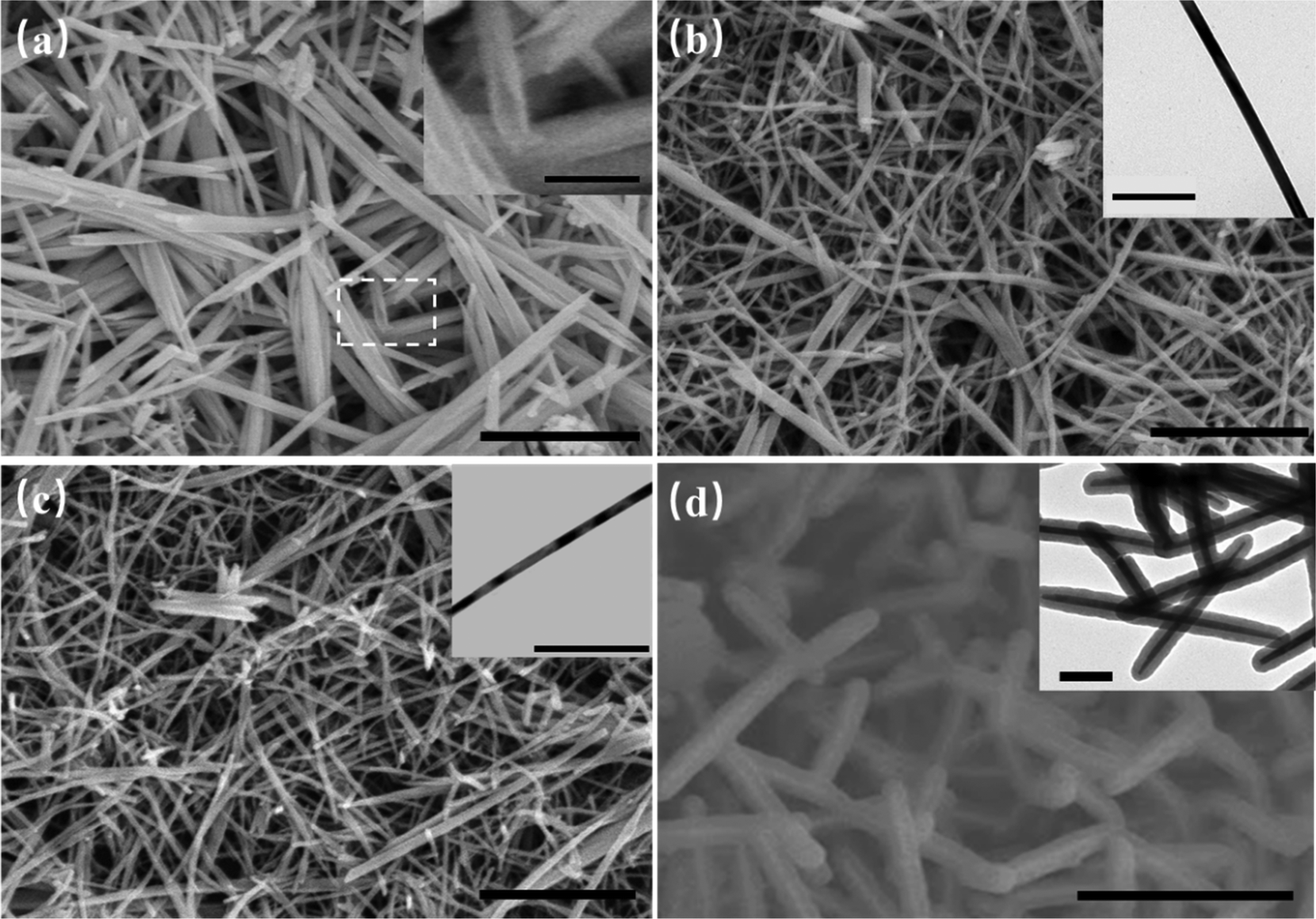 | ||
| Fig. 1 SEM images of the tellurium nanostructures prepared at different reaction temperatures. (a) At 90 °C, tellurium nanotubes were obtained. The inset is the high magnification of the shuttle-like scrolled nanotubes of tellurium. (b) and (c) At 120 °C and 150 °C, tellurium nanowires were obtained. The inset is the TEM image of tellurium nanowires. (d) At 180 °C, core/shell nanocables were synthesized. The inset is the TEM image of tellurium nanocables. Scale bar: 1 μm in the main figures and 200 nm in the insets. | ||
To further identify the characteristics of the prepared 1D Te nanostructures, a series of measurements were performed. XPS is employed to investigate the components and chemical bonding. Fig. S2 (ESI†) and Fig. 2(a), (b) show the XPS survey spectra of Te nanotubes, Te NWs, and Te nanocables. The Te 3d peaks of the Te nanotubes and nanowires exhibit apparently high intensity. In contrast, for Te nanocables, the peaks of carbon and oxygen show relatively high intensity, indicating that Te NWs are buried within the carbonaceous sheets and confirmed the Te/C nanocable structures.12,35 The high-resolution XPS spectrum of the C 1s peak is shown in Fig. S3 (ESI†), in which the peaks at 286.1 and 287.9 eV are attributed to the residue groups of C–OH and C![[double bond, length as m-dash]](https://www.rsc.org/images/entities/char_e001.gif) O.12 Because of the small detecting depth of XPS, the Te 3d peak with a binding energy of ∼573 eV for Te nanocables is nearly undetectable in Fig. 2(b) due to the existence of a carbon shell. The detailed Te 3d XPS spectrum is shown in Fig. 2(c), in which two peaks at 573 and 583 eV are assigned to the Te(0) 3d binding energy, and two relatively weak peaks at 576 eV and 586 eV can be attributed to the Te(IV) 3d binding energy. These Te 3d peaks suggest the successful synthesis of element Te in the presence of glucose reductant. XRD measurement was employed to further analyze the purity and crystallinity of these Te nanostructures. The spectra are shown in Fig. 2(d). All the diffraction peaks of these patterns can be indexed according to the trigonal structure of Te, in which the spiral chains of Te atoms are aligned parallel to each other along the longitudinal axis of each Te nanostructure.20,34,36,37 The calculated lattice constants are a = 4.4471 and c = 5.9117, which are consistent with the reported values of a = 4.468 and c = 5.927 (JPCDS card, no. 36-1452).
O.12 Because of the small detecting depth of XPS, the Te 3d peak with a binding energy of ∼573 eV for Te nanocables is nearly undetectable in Fig. 2(b) due to the existence of a carbon shell. The detailed Te 3d XPS spectrum is shown in Fig. 2(c), in which two peaks at 573 and 583 eV are assigned to the Te(0) 3d binding energy, and two relatively weak peaks at 576 eV and 586 eV can be attributed to the Te(IV) 3d binding energy. These Te 3d peaks suggest the successful synthesis of element Te in the presence of glucose reductant. XRD measurement was employed to further analyze the purity and crystallinity of these Te nanostructures. The spectra are shown in Fig. 2(d). All the diffraction peaks of these patterns can be indexed according to the trigonal structure of Te, in which the spiral chains of Te atoms are aligned parallel to each other along the longitudinal axis of each Te nanostructure.20,34,36,37 The calculated lattice constants are a = 4.4471 and c = 5.9117, which are consistent with the reported values of a = 4.468 and c = 5.927 (JPCDS card, no. 36-1452).
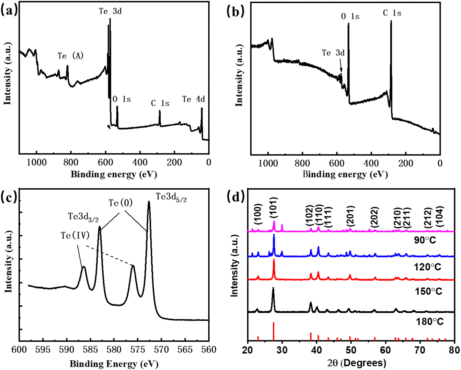 | ||
| Fig. 2 (a) and (b) Wide-range XPS spectra of the products prepared at 120 °C and 180 °C, respectively. (c) High-resolution XPS spectra of Te 3d. (d) XRD patterns of the synthesized Te nanomaterials at different reaction temperatures. | ||
The schematic diagram in Fig. 3 demonstrates the morphology-controlled synthesis process of Te 1D nanostructures. The reduction reaction can be expressed in the following equation:38
| 2CH2OH–(CHOH)4–CHO + Na2TeO3 → 2CH2OH–(CHOH)4–COONa + Te + H2O |
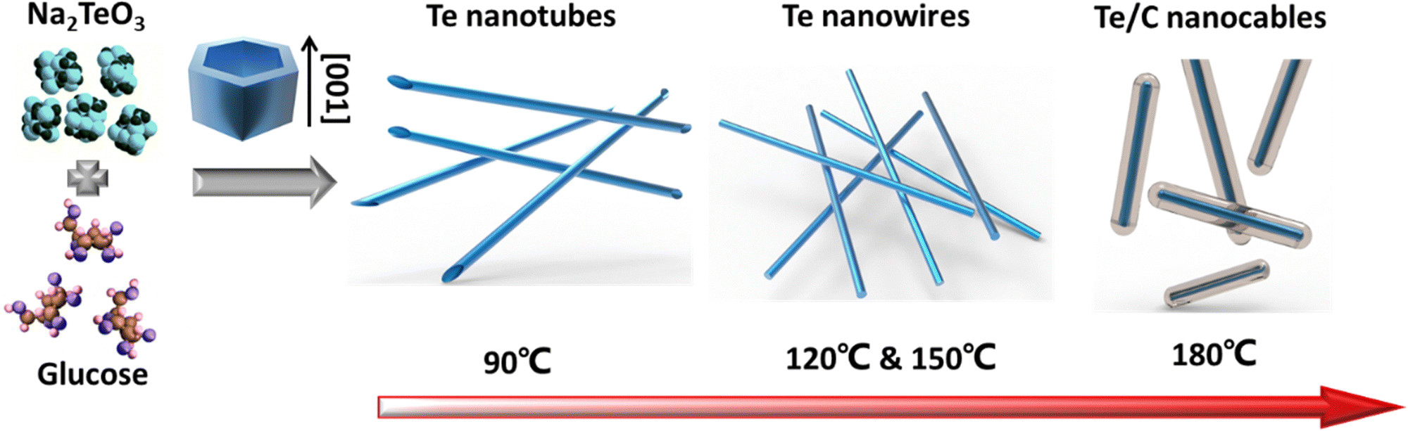 | ||
| Fig. 3 Schematic illustration of the morphology-controlled synthesis of Te 1D nanostructures. | ||
Besides 1D nanostructures, 2D tellurene can also be synthesized by this green solution process, in which shape transformation from 1D to 2D will take place with an extended reaction time in the presence of surfactants.11 By employing glucose as the reductant and surfactant, we prolonged the reaction time from 24 to 40 hours and kept other parameters unchanged. Subsequently, 2D tellurene could be examined using the Raman spectra, OM, and SEM images, as shown in Fig. S4 (ESI†). The lateral dimension of the synthesized tellurene was ∼10 μm, and the crystal structure of tellurene was identified by its three typical vibration modes located at 92, 121, and 141 cm−1.5,11
We explored the electrical properties of the synthesized Te nanostructures. Benefitting from the dual function of glucose as both the reductant and surfactant, the obtained Te nanostructures show enhanced electrical properties by eliminating the impurities induced by the addition of an extra surfactant. As demonstrated in Fig. S5 (ESI†), Te NWs show high conductivity and low transconductance (poor gate controllability), indicating the potential for transparent conductive electrode applications. Te networks were spray-coated on the SiO2 substrate in high uniformity, as shown by the SEM image in Fig. 4(a). To make up the insulated voids of Te networks at the microscopic scale, highly conductive two-dimensional MXene (Ti3C2Tx) flakes were induced. Ti3C2Tx nanoflakes were exfoliated by the typical liquid exfoliation process (details are in the Experimental section), and their XRD patterns, OM, and SEM images are shown in Fig. S6 (ESI†). The solution of the obtained Ti3C2Tx nanosheets (20 mg mL−1) was coated on the prepared Te NW networks, forming Te NWs/Ti3C2Tx hybrid structures, as demonstrated in Fig. S7 (ESI†). Fig. 4(b) shows the SEM images of the top view of Te NWs/Ti3C2Tx hybrid structures, in which Te networks are covered by Ti3C2Tx flakes. The UV-vis-NIR spectrum is utilized to investigate the optical characteristics of Te NWs/Ti3C2Tx hybrid films with different solution concentrations of Te NWs (Fig. 4(c)). A broad absorption peak at around 700 nm and an absorption peak in the UV region were verified as the typical characteristics of MXene films.41 The sheet resistances of Te NWs/Ti3C2Tx TCEs were evaluated using a sheet resistance meter. The transmittances at 550 nm wavelength and sheet resistances of Te and Te/MXene TCEs with different Te NW concentrations are shown in Fig. S8 (ESI†). With the spray-coating of the MXene layer, Te/MXene demonstrates significant performance enhancement with obvious lower sheet resistances and similar transmittances. Fig. 4(d) summarizes the transmittances and sheet resistances of Te NWs/Ti3C2Tx with different Te NW concentrations. The engagement of the Ti3C2Tx cover layer results in negligible increases of transmittances but significant reductions of sheet resistances. Finally, a low sheet resistance of 420 Ω sq−1 and a high transmittance of 70% were achieved. The solution concentration of MXene was also modulated to analyze the optoelectrical properties of Te/MXene TCEs (Fig. S9, ESI†), and a sheet resistance of 156 Ω sq−1 and a high transmittance of 70% were achieved. A comparison of various transparent conductive electrodes based on nanomaterials is shown in Table S1 (ESI†), in which the Te/MXene TCE shows an obvious advantage.
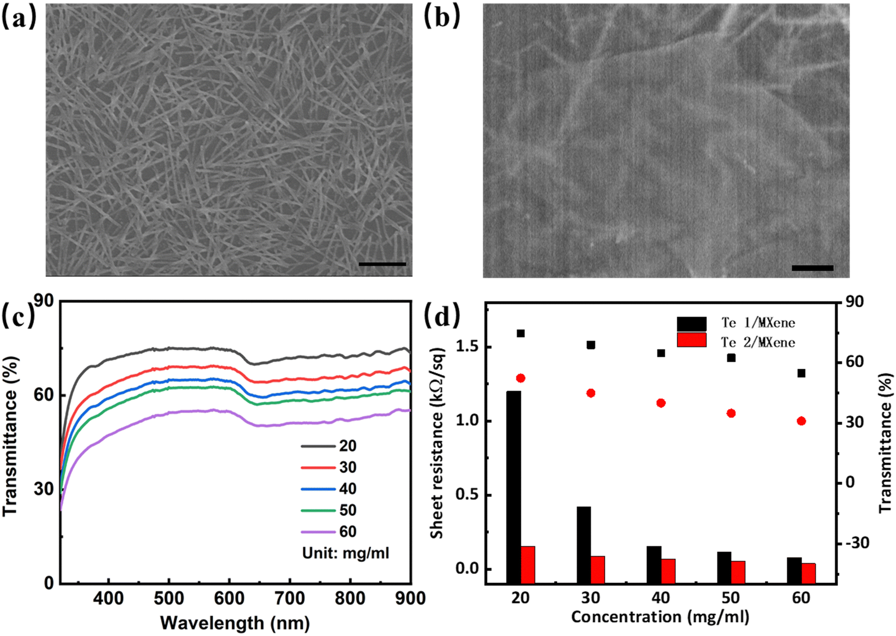 | ||
| Fig. 4 (a) and (b) SEM images of Te NW films and Te NW/MXene hybrid structures. Scale bar, 0.5 μm. (c) Transmission spectra of Te NWs/MXene hybrid structures with different solution concentrations of Te NWs. (d) Sheet resistances and transmittances of Te NWs/MXene hybrid structures with different solution concentrations of Te NWs. Te 1/MXene: Te/MXene hybrid structures with one layer of Te NWs. Te 2/MXene: Te/MXene hybrid structures with two layers of Te NWs. | ||
Conclusions
In summary, the morphology-selected synthesis of low-dimensional tellurium nanostructures is realized using a green solution process. The morphologies of the synthesized nanomaterials are determined by two process parameters: the reaction temperature and time. With the process temperature increasing from 90 °C to 180 °C, Te nanotubes, nanowires, and Te/C nanocables can be obtained, respectively. The biomolecule glucose is employed as the reductant and surfactant in the synthesis process, which avoids the addition of an extra surfactant and results in a high quality of the prepared nanomaterials. Then, a Ti3C2Tx cover layer was introduced to make up the insulated voids of a pure Te NW film and improve its stability in the air. Finally, a high-performance transparent electrode with a low sheet resistance (156 Ω sq−1) and a high transmittance (70%) was realized with a Te/MXene hybrid structure.Experimental section
Synthesis of Te nanostructures
To synthesize tellurium 1D nanostructures, sodium tellurite (Na2TeO3, ≥99%) was used as the tellurium source. Glucose was added as the reductant and surfactant. First, 2.9904 g of glucose (Analytical Reagent, AR) and 0.105 g of Na2TeO3 were mixed and dissolved in 60 mL of deionized (DI) water under stirring to form a homogeneous solution. The mixed solution was poured into a 100 mL Teflon-lined stainless-steel autoclave. The autoclave was sealed and kept at certain reaction temperatures for 12 hours. The obtained mixture was washed with DI water 3 times (centrifugation, 5000 rpm × 5 min per cycle). For the synthesis of 2D tellurene, the reaction temperature was fixed at 120 °C and the reaction was extended to 40 hours.Synthesis of MXene (Ti3C2Tx) nanosheets
1 g of Ti3AlC2 power was slowly added to a premixed etchant solution containing a lithium fluoride (LiF) salt (1.6 g) and hydrochloric acid (12 M, 30 mL). The obtained mixture was allowed to stand for 24 h at 40 °C and then washed with deionized water. With consecutive centrifugation (3500 rpm × 3 min per cycle) until the pH of the supernatant is ∼6, delamination is completed.Characterization
Scanning electron microscopy (S-4800, Hitachi) and transmission electron microscopy (JEM-1400, JEOL) measurements were performed to measure the morphologies of the synthesized Te nanostructured materials. X-ray photoelectron spectroscopy (Thermo Scientific, Thermo Fisher) was performed to understand the chemical composition of the synthesized Te nanostructure. The phase structure was characterized by X-ray diffraction (Bruker D8 advance). Raman spectra were recorded using a laser micro-Raman spectrometer (LabRAM HR Evolution, HORIBA lobin Yvon) with an excitation of a 532 nm laser. The electrical properties were measured using a Keithley 4200 parameter analyzer. Transmittances and sheet resistances were confirmed using a spectroscope (MAX 2000 pro) and a sheet resistance meter (RTS-9).Author contributions
M. Xu and L. Jiang: experiments; J. Li, J. He, and Q. Yang: analysis, writing the draft, and review. D. He, Y. Wang, and Y. Yang: conceptualization, supervision, and editing.Conflicts of interest
There are no conflicts to declare.Acknowledgements
We gratefully acknowledge support from the Fundamental Research Funds for the Central Universities 2021RC212, the National Natural Science Foundation of China (grant no. 62105018 and 61975007), and the Beijing Natural Science Foundation of China (grant no. Z190006 and 4222073).References
- H. Hu, Y. Zeng, S. Gao, R. Wang, J. Zhao, K. You, Y. Song, Q. Xiao, R. Cao, J. Li, Z. Lin, J. Guo, Y. Shu, Z. Guo and D. Fan, J. Mater. Chem. C, 2021, 9, 508–516 RSC.
- Y. Meng, X. Li, X. Kang, W. Li, W. Wang, Z. Lai, W. Wang, Q. Quan, X. Bu, S. Yip, P. Xie, D. Chen, D. Li, F. Wang, C.-F. Yeung, C. Lan, C. Liu, L. Shen, Y. Lu, F. Chen, C.-Y. Wong and J. C. Ho, Nat. Commun., 2023, 14, 2431 CrossRef CAS PubMed.
- Y.-H. Chan, C.-Y. Lin, Y.-C. Chou, A. C. Chang, Y.-F. Lin and Y.-Z. Chen, Mater. Adv., 2023, 4, 2008–2016 RSC.
- G. Qiu, C. Niu, Y. Wang, M. Si, Z. Zhang, W. Wu and P. D. Ye, Nat. Nanotechnol., 2020, 15, 585–591 CrossRef CAS.
- J. Lu, Y. He, C. Ma, Q. Ye, H. Yi, Z. Zheng, J. Yao and G. Yang, Adv. Mater., 2023, 35, 2211562 CrossRef CAS PubMed.
- Y. Zhang, F. Zhang, Y. Xu, W. Huang, L. Wu, Z. Dong, Y. Zhang, B. Dong, X. Zhang and H. Zhang, Small Methods, 2019, 3, 1900349 CrossRef CAS.
- Y. Zhang, Y. Xu, C. Zhang, J. Guo, Z. Shi, L. Wu, F. Zhang, C. Ma, R. Cao, L. Gao, Y. Ge, X. Zhang and H. Zhang, J. Mater. Chem. C, 2020, 8, 5991–6000 RSC.
- Y. Zhang, F. Zhang, L. Wu, Y. Zhang, W. Huang, Y. Tang, L. Hu, P. Huang, X. Zhang and H. Zhang, Small, 2019, 15, 1903233 CrossRef CAS.
- B. Mayers and Y. Xia, Adv. Mater., 2002, 14, 279–282 CrossRef CAS.
- Z. He, S.-H. Yu and J. Zhu, Chem. Mater., 2005, 17, 2785–2788 CrossRef CAS.
- Y. Wang, G. Qiu, R. Wang, S. Huang, Q. Wang, Y. Liu, Y. Du, W. A. Goddard, M. J. Kim, X. Xu, P. D. Ye and W. Wu, Nat. Electron., 2018, 1, 228–236 CrossRef.
- W. Wang, L. Sun, Z. Fang, L. Chen and Z. Zhang, Cryst. Growth Des., 2009, 9, 2117–2123 CrossRef CAS.
- Z. Li, S. Zheng, Y. Zhang, R. Teng, T. Huang, C. Chen and G. Lu, J. Mater. Chem. A, 2013, 1, 15046–15052 RSC.
- G. Wang, Y. Guan, Y. Wang, Y. Ding and L. Yang, Materials, 2023, 16, 738 CrossRef CAS PubMed.
- V. Adepu, M. Tathacharya, R. Cs, V. Mattela and P. Sahatiya, ACS Appl. Nano Mater., 2022, 5, 18209–18219 CrossRef CAS.
- J. Yoon, B. You, Y. Kim, J. Bak, M. Yang, J. Park, M. G. Hahm and M. Lee, ACS Appl. Mater. Interfaces, 2023, 15, 18463–18472 CrossRef CAS PubMed.
- Y. Liu, Q. Jiang, J. Zhang, W. Ding, J. Xu, P. Liu, G. Nie, H. Mao and F. Jiang, Mater. Adv., 2020, 1, 1125–1133 RSC.
- R. Zheng, K. Zheng and H. Fu, Appl. Surf. Sci., 2011, 257, 8024–8027 CrossRef CAS.
- L. Jin, Y. Hao, A. K. Tareen, K. Khan, S. Wageh, O. A. Al-Hartomy, A. G. Al-Sehemi, H. Zhang and Y. Zhang, J. Mater. Chem. A, 2023, 11, 3771–3788 RSC.
- X. Wang, Y. Xu, H. Zhu, R. Liu, H. Wang and Q. Li, CrystEngComm, 2011, 13, 2955 RSC.
- C. Shen, Y. Liu, J. Wu, C. Xu, D. Cui, Z. Li, Q. Liu, Y. Li, Y. Wang, X. Cao, H. Kumazoe, F. Shimojo, A. Krishnamoorthy, R. K. Kalia, A. Nakano, P. D. Vashishta, M. R. Amer, A. N. Abbas, H. Wang, W. Wu and C. Zhou, ACS Nano, 2019, 14, 303–310 CrossRef PubMed.
- C. Liu, R. Wang and Y. Zhang, Nanomaterials, 2022, 12, 2151 CrossRef CAS PubMed.
- Y. Zhang, J. Guo, Y. Xu, W. Huang, C. Li, L. Gao, L. Wu, Z. Shi, C. Ma, Y. Ge, X. Zhang and H. Zhang, Nanoscale Horiz., 2020, 5, 847–856 RSC.
- D. Choi, D. Kim, Y. Jo, J. H. Kim, E. Yoon, H.-C. Lee and T. Kim, Appl. Surf. Sci., 2021, 565, 150521 CrossRef CAS.
- X. Wei, S. Wang, N. Zhang, Y. Li, Y. Tang, H. Jing, J. Lu, Z. Xu and H. Xu, Adv. Funct. Mater., 2023, 33, 2300141 CrossRef CAS.
- M. Xu, J. Xu, L. Luo, M. Wu, B. Tang, L. Li, Q. Lu, W. Li, H. Ying, L. Zheng, H. Wu, Q. Li, H. Jiang, J. Di, W. Zhao, Z. Zhang, Y. He, X. Zheng, X. Gan, Z. Liu, X. Wang and W. Huang, Mater. Today, 2023, 63, 50–58 CrossRef CAS.
- Y. Ahn, D. Lee, Y. Jeong, H. Lee and Y. Lee, J. Mater. Chem. C, 2017, 5, 2425–2431 RSC.
- H. Ding, Y. Li, M. Li, K. Chen, K. Liang, G. Chen, J. Lu, J. Palisaitis, P. O. Persson and P. J. S. Eklund, Science, 2023, 379, 1130–1135 CrossRef CAS PubMed.
- K. R. G. Lim, M. Shekhirev, B. C. Wyatt, B. Anasori, Y. Gogotsi and Z. W. Seh, Nat. Synth., 2022, 1, 601–614 CrossRef.
- A. VahidMohammadi, J. Rosen and Y. Gogotsi, Science, 2021, 372, 1165 CrossRef PubMed.
- Y. Liu, X. Zhang, W. Zhang, X. Ge, Y. Wang, X. Zou, X. Zhou and W. Zheng, Energy Environ. Mater., 2022, e12438 CrossRef.
- J. Li, W. Zhang, X. Ge, M. Lu, X. Xue, Z. Wang, N. Yue, J. Zhang, X. Lang, Q. Jiang and W. Zheng, J. Energy Chem., 2022, 72, 26–32 CrossRef CAS.
- E.-Y. Shin, S. B. Choi, J. H. Lee, B. Yoo, C. J. Han, S. H. Park, J. H. Noh, J.-W. Kim and H. J. Son, Sol. RRL, 2023, 7, 2201130 CrossRef CAS.
- G. S. Cao, C. W. Dong, L. Wang and Z. S. Liu, Mater. Lett., 2009, 63, 1778–1780 CrossRef CAS.
- G. Xi, C. Wang, X. Wang, Y. Qian and H. Xiao, J. Phys. Chem. C, 2008, 112, 965–971 CrossRef CAS.
- G. S. Cao,Y., G. Liu, W. W. Yang, C. Tan, H. Li and X. J. Zhang, Bull. Mater. Sci., 2011, 34, 1185–1188 CrossRef.
- J. Chen, Y. Gao, J. Yang, Q. Wang, Y. Cao, K. Jiang, Y. Li, J. Zhang, L. Zhu, L. Shang, Z. Hu and J. Chu, IEEE Electron Device Lett., 2022, 43, 1776–1779 CAS.
- Q. Chen, G. Liu, G. Chen, T. Mi and J. J. B. Tai, BioResources, 2017, 12, 608–621 CAS.
- Z. Liu, S. Li, Y. Yang, Z. Hu, S. Peng, J. Liang and Y. Qian, New J. Chem., 2003, 27, 1748 RSC.
- G. Krueger and C. J. T. J. o C. P. Miller, J. Chem. Phys., 1953, 21, 2018–2023 CrossRef CAS.
- P. Salles, D. Pinto, K. Hantanasirisakul, K. Maleski, C. E. Shuck and Y. Gogotsi, Adv. Funct. Mater., 2019, 29, 1809223 CrossRef.
Footnotes |
| † Electronic supplementary information (ESI) available. See DOI: https://doi.org/10.1039/d3ma00579h |
| ‡ These authors contributed equally to this work. |
| This journal is © The Royal Society of Chemistry 2023 |