 Open Access Article
 This Open Access Article is licensed under a
 Creative Commons Attribution 3.0 Unported Licence
Vapor–liquid–solid growth of serrated GaN nanowires: shape selection driven by kinetic frustration†
Zheng Maa, Dillon McDowella, Eugen Panaitescua, Albert V. Davydovb, Moneesh Upmanyu*cd and Latika Menon*a
aDepartment of Physics, Northeastern University, Boston, MA 02115, USA. E-mail: l.menon@neu.edu
bMaterial Measurement Laboratory, National Institute of Standards and Technology, Gaithersburg, Maryland 20899, USA
cGroup for Simulation and Theory of Atomic-Scale Material Phenomena (stAMP), Department of Mechanical and Industrial Engineering, Northeastern University, Boston, MA 02115, USA. E-mail: m.upmanyu@neu.edu
dDepartment of Bioengineering, Northeastern University, Boston, MA 02115, USA
First published on 1st October 2013
Abstract
Compound semiconducting nanowires are promising building blocks for several nanoelectronic devices yet the inability to reliably control their growth morphology is a major challenge. Here, we report the Au-catalyzed vapor–liquid–solid (VLS) growth of GaN nanowires with controlled growth direction, surface polarity and surface roughness. We develop a theoretical model that relates the growth form to the kinetic frustration induced by variations in the V(N)/III(Ga) ratio across the growing nanowire front. The model predictions are validated by the trends in the as-grown morphologies induced by systematic variations in the catalyst particle size and processing conditions. The principles of shape selection highlighted by our study pave the way for morphological control of technologically relevant compound semiconductor nanowires.
The vapor–liquid–solid (VLS) route for high-yield nanowire synthesis allows control over the growth form and composition via a capping catalyst particle that serves both as a catalyst and conduit for material transfer onto the growing wire.1–5 The size of the particle is the primary length-scale that controls the nanowire diameter while the time-scale is usually set by a combination of slow surface catalysis and nucleation at the catalyst–nanowire interface.6–8 In the case of compound semiconductors, the growth morphology of thin films is strongly influenced by the relative rates of incorporation of the constituent species,9 and such effects must also modify growth of nanowires. Indeed, recent studies on semiconducting III–V and II–VI nanowires have shown that the incorporation ratio has a direct effect on their growth rate and crystal quality,10–12 yet the fundamental mechanisms that affect the growth energetics and kinetics remain unknown. In this article, we systematically explore this interplay during Au-catalyzed growth of GaN nanowires, a wide band-gap material of direct relevance in optoelectronics and power nanoelectronics.13–15 The combination of experiments and theoretical frameworks identify a novel mechanism for shape selection in GaN nanowires based on an interplay between surface energetics and catalytic kinetics, with broad implications for controlled growth of vertical arrays of compound nanowires.
The nanowires are grown by ammoniating solid Ga2O3 over an Au-decorated 〈100〉 Si substrate at temperature T = 960 °C and pressure P = 100 Torr (see Methods). Under these conditions, the use of hydrogen as a carrier gas results in Ga2O3 vapor pressure that is readily abstracted by the flowing NH3 gas to elemental Ga and N.16–19 The growth is evident in the low-resolution SEM image (Fig. 1a). Almost all nanowires are capped by a Au particle characteristic of the classical vapor–liquid–solid (VLS) growth mechanism. Uncatalyzed vapor–solid (VS) lateral growth of the nanowires is much slower and effectively suppressed under these conditions,17,20–23 a fact further validated by negligible diameter coarsening upon varying the exposure time (not shown). X-ray diffraction of the as-grown nanowires confirms that they are strain-free hexagonal wurtzite crystals (ESI, Fig. S1†).
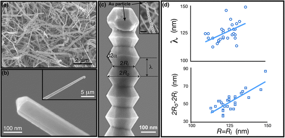 | ||
| Fig. 1 Morphology of as-synthesized GaN nanowires: (a) SEM characterization of Au-catalyzed GaN nanowires grown via chemical vapor deposition at temperature T = 960 °C and pressure P = 100 Torr. The Ga partial pressure corresponds to the initial mass m = 1.02 g of the solid precursor Ga2O3. Approximately 15% of the as-grown nanowires are serrated. (b) High-resolution image of a straight nanowire with the exposed growth front that reveals a triangular cross-section. (inset) Low-resolution image showing the smooth lateral facets and the capping catalyst particle. (c) Low- (inset, scale bar 200 nm) and high-resolution image of a serrated GaN nanowire capped by an Au-catalyst particle. The parameters associated with the nanowire morphology are as indicated: 2Ri = 125 nm 2Ro = 200 nm, λ = 120 nm, and α ≈ 60°. (d) Size dependence of the wavelength λ (top) and amplitude 2Ro − 2Ri (bottom) associated with the serrations. | ||
The as-grown morphology consist of straight nanowires with smooth sidewalls as well as several instances of rough yet highly periodic surface morphologies. Higher resolution SEM images of the smooth nanowires are shown in Fig. 1b. The nanowire radius is approximately that of the catalyst particle during axial growth (inset). In some cases, the droplet etches away and exposes a triangular nanowire cross-section, evident in the figure. Lattice fringes with inter-planar distance d ≈ 2.78 Å are visible in HRTEM image normal to the growth axis (ESI, Fig. S2†). Secondary fringes aligned 30° to the wire axis are also evident as indicated. We rarely see any interruptions in the fringes indicating that the nanowires are largely defect-free. Taken in toto, the nanowire is composed of non-polar m-planes stacked along the 〈10![[1 with combining macron]](https://www.rsc.org/images/entities/char_0031_0304.gif) 0〉 direction. For a nanowire so grown, one of the three lateral facets is the polar {0001} plane and the other two belong to the 〈11
0〉 direction. For a nanowire so grown, one of the three lateral facets is the polar {0001} plane and the other two belong to the 〈11![[2 with combining macron]](https://www.rsc.org/images/entities/char_0032_0304.gif) 2〉 family of directions. The non-polar growth is classical in that it has been reported under a variety of conditions and several synthesis techniques,24 including the VLS route.25,26
2〉 family of directions. The non-polar growth is classical in that it has been reported under a variety of conditions and several synthesis techniques,24 including the VLS route.25,26
Of interest is the serrated morphology and the conditions that stabilize its growth. Majority of these serrated nanowires have larger diameter. The SEM images in Fig. 1c show the detailed view of the nanowire morphology. The growth of these nanowires is also via the VLS mechanism as the nanowire is always capped with the Au particle. Fig. 2a shows another example with a stable Au particle. Although the catalyst particle is faceted at room temperature, the high growth temperature Au–Ga solution forms a melt for Ga concentrations above a critical value. This follows from the phase diagram which predicts a stable liquid Au–Ga solution for Ga concentrations above 5 at%.27,28 The critical composition is size dependent yet the growth form is unaffected as the corrections simply scale the critical Ga composition.
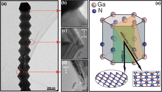 | ||
| Fig. 2 Characterization of serrated nanowires: (a) Low-resolution TEM image of a serrated nanowire. (b) The magnified view of the particle-nanowire interface near the contact line. The image is tilted slightly with respect to (a) for clarity. (c and d) Magnified views of the intersection of the two facets as indicated by the arrows. The scale bar is 5 nm. The fringes in (c) and (d) correspond to planes normal to the growth direction. The average inter-planar spacing of d = 2.63 Å is consistent with growth along the polar 〈0001〉 direction. (e) The hexagonal wurtzite GaN unit cell. The non-polar m-plane (shaded green) and the semi-polar {101} plane (shaded orange) are shown as reference. The insets show the unreconstructed semi-polar surface structure observed along two orthogonal directions indicated by arrows. | ||
The size of the catalyst particle is approximately the average nanowire diameter. The low-resolution image in the inset shows that the nanowire maintains its hexagonal cross-section. The lateral facets, visible in the magnified image are consistent with the six-fold symmetry and give an appearance of truncated hexagonal bipyramids stacked along the growth direction. The serrations are remarkably periodic; for a given nanowire radius Ri the wavelength λ and the amplitude 2A = (Ro − Ri) are both preserved along the length of the nanowire. The facet reorientation angle 2α is also preserved but it is independent of the nanowire size, i.e. 2α ≈ 120° averaged several nanowire segments.
HRTEM characterization of the serrations shown in Fig. 2 do not indicate the presence of any obvious defects/grain boundaries. Rather, the lattice fringes are unbroken and continue across the serrations indicating that the nanowire is a high quality single crystal. This crystalline nature is also preserved at points where the sidewall facets reorient (Fig. 2c and d). Viewed approximately normal to the growth axis we see lattice fringes with clear variations in grayscale contrast. The fringe spacing d ≈ 2.63 Å is consistent with growth of polar bilayers along the 〈0001〉 direction (c-axis). Unlike classical polar growth, though, the enveloping sidewall facets are inclined at an angle α ≈ 60° for each facet which we then identify to be the {101} or {112} family of planes. Selective area electron backscatter diffraction (EBSD) analysis of serrated segments confirms the 〈0001〉 growth direction and identifies the orientation of the semi-polar planes that form the sidewall facets of the truncated hexagonal bipyramid segments to be the {101} family of planes; the analysis is detailed in ESI, Fig. 3.† The wurtzite unit cell drawn schematically in Fig. 2e shows the details of the crystallographic relationship for one of the six semi-polar planes. The atomic configurations of the (unreconstructed) N-polar surface structure viewed along two orthogonal directions are also shown in the insets.
The serrated morphology depends on the nanowire size and the variation is plotted in Fig. 1d. Although there is scatter, both λs and 2A increase with the nanowire size Ri. A linear fit to our data yields λ ≈ 0.85Ri. The amplitude of the serrations varies as 2A ≈ Ri and yields the wavelength/amplitude ratio, λ/A ≈ 1.7. The ratio is remarkably small indicating a fully faceted yet extremely rough morphology which can be tuned simply by changing the nanowire size.
A careful examination of the as-grown samples also reveals transitions between the two growth morphologies. Several instances of serrated-to-smooth transitions are highlighted in Fig. 3a (encircled, left and middle panels). We have also carried out EBSD analysis transition zones and the results are shown in ESI, Fig. 3.† The change in growth morphology is preceded by a gradually tapering cross-section, i.e. the dynamic transitions are strongly correlated with decrease in the nanowire size. The tapering is most likely due to a decrease in the catalyst particle size during growth as the Au atoms diffuse down the nanowire sidewalls.29 In each case, the effective nanowire growth direction changes (top right). Closer examination shows that the transition point consists of a series of visibly discrete kinks consisting of increasingly truncated bipyramids such that the effective growth direction is along intermediate, low-energy orientations (right, bottom). Although the crystallographic orientation of each of the kinks is still polar, the effective orientation of these transition zones is semi-polar. In essence, the kinking reflects local variations in processing conditions and/or geometry that modify the growth direction as well as the nanowire morphology.
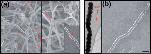 | ||
| Fig. 3 Variations and transitions in GaN nanowire growth morphology: (a) SEM images showing serrated-to-smooth shape transitions, the scale bar is 200 nm. (left and middle) Circled regions indicating distinct reduction in the nanowire diameter accompanying the transition. (top and bottom, right) Early stages of the transition to a non-polar growth direction with smooth sidewall morphology. The encircled region (bottom) shows the discrete kinks consisting of truncated bipyramids. (b) Local and reversible morphology changes seen in low-resolution TEM image (left) and high resolution SEM images (right). | ||
We see similar kinks within confined regions in an otherwise serrated nanowire (Fig. 3b). Evidently, the change in the growth direction is not dynamically stable as the nanowire reverts back to its original growth direction. There is negligible change in the nanowire size (left and top right panels) and detailed characterization of the transition zone shows modified serrations due to the intermediate semi-polar growth orientation/s (bottom right panel). We note that majority of the transition are observed at relatively large Ga partial pressures (higher mass of solid Ga2O3), and we do not observe smooth-to-serrated transitions.
The interplay between the growth direction and the V![[thin space (1/6-em)]](https://www.rsc.org/images/entities/char_2009.gif) :III ratio is consistent with several past studies on GaN thin films and nanowires.17,30,31 The non-polar growth direction is favored for ratios close to unity. This indicates that the combination of growth parameters that result in growth of the 〈100〉 non-polar nanowires is such that the V:III ratio at the growth front is close to unity. Reducing the amount of Ga in the gas phase increases the V:III ratio at the growth front and the growth direction switches to the 〈0001〉 polar direction.
:III ratio is consistent with several past studies on GaN thin films and nanowires.17,30,31 The non-polar growth direction is favored for ratios close to unity. This indicates that the combination of growth parameters that result in growth of the 〈100〉 non-polar nanowires is such that the V:III ratio at the growth front is close to unity. Reducing the amount of Ga in the gas phase increases the V:III ratio at the growth front and the growth direction switches to the 〈0001〉 polar direction.
The serrated morphology of the polar nanowires is unlike past reports of the rough morphologies observed during VS growth. The surface roughness there is controlled by the Ga diffusion length that is directly influenced by the V:III ratio; low ratios result in smooth morphologies while large ratios lead to surface roughening as the Ga diffusion length at the crystal–vapor interface is dramatically reduced by N-rich conditions.17 This is in direct contrast to the our observations as the serrations occur under N-deficient conditions. Evidently, the droplet and the solid–liquid interface plays a central role in the combined interplay between the size, interface energetics and kinetics during the morphological evolution of the nanowire.
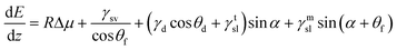
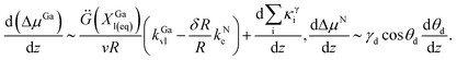
Development of a detailed theoretical model is handicapped by the lack of quantitative understanding of these aspects in GaN in particular and multicomponent systems in general, and we present a simplified analysis of the competing effects. Current understanding of the interplay between size and energetics during general VLS growth revolves around the interfacial balance at the vapor–particle–nanowire trijunction.6,32–39 The serrations are reminiscent of similar growth form observed during VLS growth of Si(111) nanowires marked by absence of low-energy facets normal to the growth direction. Then, surface energy considerations alone force the nanowire size to shrink or widen to accommodate the low-energy inclined facets as illustrated schematically in Fig. 4a. The size cannot change monotonically since it is constrained by the wetting angle between the droplet and the nanowire along the contact line. As the nanowire widens or narrows, the droplet is stretched and compressed respectively. Beyond a critical size, the pressure exerted by droplet forces the sidewalls to reorient at regular intervals. Ross et al. have recently analyzed this interplay between geometry and energetics for 2D near-equilibrium nanowire growth based on a balance between (i) changes in the surface and (nanowire-particle) interphase area, and (ii) the work done against the surface tension γd of an almost hemispherical particle.40 The angle θf between the facets and the growth axis is fixed as the shrinking and growing facets belong to the same family of planes. Then, the wavelength of the serrations varies as40
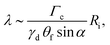 | (1) |
 | ||
| Fig. 4 Growth model: (a) schematic showing the evolution of the droplet-nanowire system as the size oscillates. The interplay between size dependent droplet supersaturation and the fully faceted morphology of the droplet-nanowire interface is shown. (a) Schematic showing the main elements of the theoretical model that relates the size and the V:III ratio to the growth morphology of the serrated nanowire. The nitrogen incorporation is assumed to occur over an exposed annular ring (thickness δR) enveloping the contact line (shaded blue), which also serves as the preferred site for GaN nucleation as illustrated. (c and d) The energetics at the contact line during (c) the widening (d) and narrowing phases of the growth. The colored regions near the contact line represent the volume swept out by the truncating facets during each oscillatory growth cycle. The dark solid and dotted lines represent the initial and final states of the droplet and the sidewall facets, respectively. The lightly shaded dotted line in (d) is an alternate concave morphology of the solid–liquid interface that is also possible as the sidewalls narrow inwards. See text for details. | ||
There is considerable scatter in the size dependence, though, and that is likely due to several oversimplying assumptions. One, the model assumes that the nanowire-particle interface is flat. Recent studies have shown that is not the case, rather the interface is enveloped by truncating facets as it meets the contact line.41–44 The fully faceted morphology is shown schematically in Fig. 4a. Note that the equilibrium Wulff plot associated with the inclination dependent solid–liquid interface energy determines the relative areas of the two classes of facets. Following ref. 35, the change in energy of the nanowire per unit length of growth becomes
 | (2) |
The second assumption relates to the chemical potential difference Δμ between the solid nanowire and supersaturated droplet that drives the nanowire growth. The is a key issue as N has negligible solubility within the Au particle28 and its catalysis is limited to the contact line, approximated as an annular ring of width δR. Ga incorporation, on the other hand, occurs through the particle as Au not only catalyzes the decomposition of the Ga precursor but also forms a stable Au–Ga solution.27 The scenario is shown schematically in Fig. 4b. Then, the size of the Au-particle impacts the V:III ratio at the growth front in that the atomic incorporation rates ![[scr I, script letter I]](https://www.rsc.org/images/entities/char_e143.gif) Ga and N scale differently with the catalyst particle size, R. Ignoring differences in the atomic volume of Ga and N across the phases, the steady-state supersaturation at the growth front evolves as (see ESI, eqn S1–S8†)
Ga and N scale differently with the catalyst particle size, R. Ignoring differences in the atomic volume of Ga and N across the phases, the steady-state supersaturation at the growth front evolves as (see ESI, eqn S1–S8†)
 | (3) |
 | (4) |
The scaling relations ((3) and (4)) capture the main effect of size on the asymmetry in the build up of excess Ga and N and therefore the V:III ratio at the growth front. This has a direct effect on the driving force as both the Ga and N chemical potentials are related to their supersaturation. Consider the extreme case where the N-supply sets the overall nanowire growth velocity. Then, the excess N-coverage along the contact line is negligible such that dXNc/dz ≈ 0 and eqn (4) reduces to
 | (5) |
Then, the periodic modulations in the nanowire size during serrated growth are coupled to oscillations in Ga supersaturation in the droplet and therefore the overall V:III ratio at the growth front (ESI, eqn (16)†). Specifically,
 | (6) |
The second term in ΔμGa is the contribution from the weighted mean curvatures of the two classes of facets that make up the nanowire-particle interface.48,49 It is directly related to the relative lengths (areas) of the facets. In essence, its effect is such that chemical potential in the droplet varies inversely with the extent of truncation.42 Observe that μNc is regulated by the droplet contact angle. The combined effect results in a non-trivial interplay between the net driving force Δμ = XGaGaNΔμGal + XNGaNΔμNc and the energy minimizing sidewall facet given by minimization of eqn (2).
The analysis is consistent with recent experiments that have shown direct correlation between the V:III ratio and changes in nanowire size.50 The size change is believed to be entirely due to change in droplet size, i.e. there the kinetics results in an interplay between the V:III ratio and the droplet size Unlike these studies, though, the highly periodic modulations we observe here indicate a self-regulating mechanism which follows directly from size controlled chemical potential variations within the liquid droplet. More concretely, the growth of large diameter nanowires is nitrogen deficient which initially leads to diameter reduction along the energy minimizing facet orientation of the sidewalls, i.e. the sidewall shape selection is no longer governed completely by interface energetics. It is now modified by kinetics since it must also increase the V:III ratio while maintaining growth along the c-axis. Note that if ignore the much smaller changes in the droplet size, the droplet angle θd increases as the droplet is squeezed in and this enhances the μNc. At a critical point, the V:III ratio increases to close to unity. The nanowire can change its growth direction to non-polar growth, and we see successful as well as failed attempts at these transitions in Fig. 3. Clearly, there is an energy barrier that needs to be overcome to effect the growth direction change. The barrier for changing the growth direction is expectedly smaller than that for reorientation of the sidewall facets, and the nanowire starts to widen by reorienting the sidewall facets which also alleviates the compression in the droplet. At this point, the Ga supersaturation in the droplet is at a minimum as the difference in the effect the effective catalysis rates kGavl − (δR/R)kNc decreases with size. Then, the nanowire-particle interface is significantly truncated as shown in Fig. 4a. The widening of the sidewalls again minimizes the interface energies and occurs along the direction that rectifies the Ga deficiency. The droplet becomes increasingly stretched and at a critical point the capillary forces favor narrowing of the sidewall facets. The nanowire again reorients. The droplet is significantly Ga-rich and that minimizes the lengths (areas) of the truncating facets. As mentioned earlier, the reorientation into the narrowing sidewalls can lead to a faceted yet concave morphology, as shown in Fig. 4d (lightly shaded). This not at odds with the Gibbs–Thomson effect associated with the solid–liquid interface as the droplet is significantly N-deficient and therefore undercooled with respect to the solid nanowire.49 Although we do not have direct evidence during growth, 2b does suggest a concave interfacial morphology near the contact line.
The kinetic anisotropy of the growth rates can also dictate the shape selection of the sidewall facets. This follows from the fact that non-polar planes normal to the to c-axis do exist, and we generally expect these to be lower in energy compared to the semi-polar surfaces. This is by no means conclusive as it is well-known that relative energies are sensitive to the reactor conditions including the V:III ratio and the partial pressures in the gas phase. Nevertheless, selected area growth (SAG) experiments on c+ axis GaN crystals show that under N-deficient conditions, the growth is dominated by the very same semi-polar sidewalls.51 Current understanding of the shape selection during vapor–solid (VS) crystal growth is based on the kinetic Wulff-plots that can completely dominate the growth form for large kinetic undercoolings that scale as Δμ = v/M, with M the mobility of the growth front.52 The serrated growth occurs through a Ga-rich droplet under N-deficient conditions, and therefore we expect c+ (Ga) growth for which the 〈101〉 planes have been observed to the slowest growing and therefore the dominate the sidewalls during growth of the convex and faceted solid–liquid interface. Interestingly, SAG experiments on annular rings reveal that the concave growth is dominated by 〈112〉 semi polar facets since they are the fastest growing facets.51 Although there is overwhelming evidence that the sidewall facets in the serrated nanowires here are enveloped by the 〈101〉 planes, we cannot completely rule out the presence of 〈112〉 planes as they have approximately the similar inclination to the c-axis (28° versus 32°). Then, the inclination dependent kinetic anisotropy in the growth rates solid–liquid interface would become important. The sidewall orientation selection occurs during crystallization from the droplet, and more specifically during each oscillatory cycle of growth consisting of increase and decrease in the extent of the truncating facets which eventually leads to the nucleation of a new layer on the main facet.41,42 The truncating facets maintain their orientation as they change their size and the contact line moves up and down the sidewalls during growth cycle. This is shown schematically in Fig. 4c and d. As reference, the path traced by the contact line for straight and narrowing/widening sidewalls are also shown. Then, for convex growth, the kinetic anisotropy will pick the 〈101〉 provided it is the slowest moving solid–liquid interface inclination for the range of all possible orientations that preserve c+ polar growth.
Although it is clear that kinetic frustration modifies the principles of shape selection in the serrated nanowires, a quantitative understanding of the anisotropic energetics and kinetics of solid–liquid and solid–vapor interfaces is essential to develop a more concrete understanding of GaN nanowire growth. To test several elements of our model, we have repeated our growth experiments with (i) varying average Au seed particle sizes, and (ii) varying V:III ratio. In each case, we report the yield of serrated nanowires over the entire growth region. Fig. 5 shows SEM images of the nanowires under varying growth conditions. A two-fold increase in the Au particle size results in an almost three-fold increase in the yield of serrated nanowires, showing a clear correlation between the growing particle size and the nanowire morphology. Similarly, decreasing the V:III ratio by increasing the mass of the precursor oxide results in significant increase in the yield of the serrated nanowires indicating the N-deficiency promotes the formation of the serrations. At very low ratios (Fig. 5f), the growth is sporadic and marks an upper limit for VLS growth. More importantly, both trends are consistent with the main elements of the growth model, and we expect the interplay between size, component ratio and growth morphology to be a general aspect of VLS growth of multicomponent nanowires.
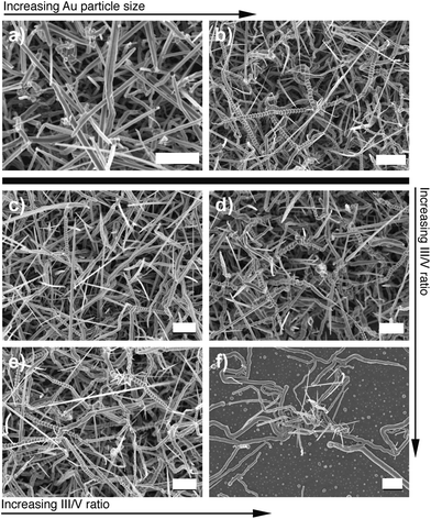 | ||
| Fig. 5 Interplay between particle size and III/V ratio and growth morphology: (a)–(b) Effect of Au catalyst size at fixed Ga2O3 partial pressure, m = 1.02 g. (a) The serrated morphology is noticeably absent for small sizes (R ≈ 80 nm) and dominates much of the as-synthesized network at larger sizes (R > 100 nm). (c–f) Effect of increasing partial pressure of Ga2O3; the input mass for the four cases are m = 0.61 g, m = 0.75 g, m = 1.03 g and m = 1.91 g, respectively. | ||
Discussion and conclusions
Our study highlights the potential of VLS route for concurrent control over the growth direction and morphology of multicomponent nanowires. The interplay between catalyst particle size and the V:III ratio can be further tuned by the controlling the growth temperature, and although this remains to be explored systematically, we expect a considerably rich set of growth morphologies. Control over the surface roughness has important ramifications for their properties. For example, nanowires of these wide band-gap materials hold promise as active materials in solar cells, light emitting diodes, and high-fidelity sensors. For most of these applications, a common desirable feature is the enhancement of the effective surface area. This increase in effective surface area can result in enhanced solar energy absorption (in solar cells) and enhanced electron–hole pair generation (in both solar cells and LEDs). While the one-dimensional nanowire morphology naturally presents enhanced effective surface areas spanning the entire cylindrical surface, this may be further enhanced by modulating the diameter along the length of the wire. Periodic diameter modulation demonstrated here can also lead to additional benefits such as reduced reflections from the surface thus enhancing the absorption,53 and to reduced thermal conductivity for thermoelectric applications.54In addition to roughness, control over the surface structure and polarity can enable novel applications. For example, Chin et al.55 have observed crystal orientation dependent photoluminescence (PL) effects in GaN nanowires. Surface states are known to act as traps of photoexcited carriers. By controlling the morphology of the nanowires and their growth direction, we have tighter control of such PL phenomena that can lead to better performance of lasers and LEDs based on GaN and related compound semiconductor nanowires.
The transitions in the growth direction can lead to nanowires with engineered interfaces which can also be used as single nanowire devices. We observe transitions from the polar growth direction (serrated nanowires) to non-polar (straight nanowires) (see also ESI, Fig. S3 and S4†). The transitions are associated with semi-polar segments, and the polarity-dependent anisotropic transport response can be engineered for a range of nanoelectronic and optical devices based on individual nanowires. Further investigations of external and local growth parameters favoring this transitional growth can even lead to control over the semi-polar growth mode that remains to be realized.
In summary, this study highlights a simple route for VLS growth of GaN nanowires with controlled growth direction, surface polarity and surface roughness. Specifically, we realize an axially serrated morphology for a specific set of growth conditions. The growth morphology is attractive for a host of applications as (i) it provides enhanced active surface with controlled surface roughness and polarity for specific applications, and (ii) it has been achieved by controlling two growth parameters, namely the initial catalyst size and the initial V:III ratio. A theoretical model shows that the newly discovered growth mode arises due to kinetic frustration at the growth front, which in turn is induced by energetic and geometric constraints. The model predictions are validated by the trends in the as-grown morphologies induced by systematic variations in the catalyst particle geometry and processing conditions. The principles of shape selection of nanowires that we uncover are directly relevant for scalable and controlled growth of wide range of technologically relevant multicomponent nanowires.
Methods
The GaN nanowires were synthesized using a chemical vapor deposition (CVD) method. A 5–11 nm thick Au catalyst films were deposited by thermal or e-beam evaporation onto Si 〈100〉 substrates. The samples were subsequently placed in the center of a 35 mm ID quartz tube, in a hot-wall CVD system, about 2 cm downstream from the gallium source (Ga2O3 powder, 99.999% purity, Alfa Aesar). The VLS growth of GaN nanowires was carried out for 1 hour at fixed temperature (960 °C) and pressure (100 Torr) conditions, while flowing a mixture of NH3 (30 sccm, the nitrogen source) and H2 (50 sccm, carrying gas) through the system. The heating and cooling were performed in an inert atmosphere with a flow rate of Ar of 70 sccm. The ammonia and hydrogen lines were kept open only during nanowire growth, after thermal equilibrium was reached at 960 °C, and correspondingly the argon line was open only during heating and cooling. Separate study of the Au catalyst particle formation as a result of thin film dewetting during annealing was carried out under the same temperature and pressure conditions, but only in argon atmosphere, without the gallium and nitrogen sources, and without flowing hydrogen.Acknowledgements
The experimental component of this work was performed under the auspices of the National Science Foundation (NSF)-ECCS Program #0925285 (ZM, EP and LM). MU acknowledges support from NSF-DMR CMMT Program #1106214. Certain commercial equipment, instruments, or materials are identified in this document. Such identification does not imply recommendation or endorsement by the National Institute of Standards and Technology, nor does it imply that the products identified are necessarily the best available for the purpose.References
- R. S. Wagner and W. C. Ellis, Vapor–liquid–solid mechanism of single crystal growth, Appl. Phys. Lett., 1964, 4, 89–90 CrossRef CAS.
- C. M. Lieber, One-dimensional nanostructures: chemistry, physics and applications, Solid State Commun., 1998, 107, 607–616 CrossRef CAS.
- X. F. Duan and C. M. Lieber, General synthesis of compound semiconductor nanowires, Adv. Mater., 2000, 12, 298–302 CrossRef CAS.
- Y. Cui, L. J. Lauhon, M. S. Gudiksen, J. F. Wang and C. M. Lieber, Diameter-controlled synthesis of single-crystal silicon nanowires, Appl. Phys. Lett., 2001, 78, 2214–2216 CrossRef CAS.
- V. G. Dubrovskii, N. V. Sibirev, G. E. Cirlin, J. C. Harmand and V. M. Ustinov, Theoretical analysis of the vapor–liquid–solid mechanism of nanowire growth during molecular beam epitaxy, Phys. Rev. E: Stat., Nonlinear, Soft Matter Phys., 2006, 73, 021603 CrossRef CAS PubMed.
- S. Kodambaka, J. Tersoff, M. C. Reuter and F. M. Ross, Diameter-independent kinetics in the vapor–liquid–solid growth of Si nanowires, Phys. Rev. Lett., 2006, 96, 096105 CrossRef CAS PubMed.
- B. J. Kim, J. Tersoff, S. Kodambaka, M. C. Reuter, E. A. Stach and F. M. Ross, Kinetics of individual nucleation events observed in nanoscale vapor–liquid–solid growth, Science, 2008, 322, 1070–1073 CrossRef CAS PubMed.
- F. M. Ross, Controlling nanowire structures through real time growth studies, Rep. Prog. Phys., 2010, 73, 114501 CrossRef.
- S. Schwaiger, S. Metzner, T. Wunderer, I. Argut, J. Thalmair, F. Lipski, M. Wieneke, J. Blasing, F. Bertram, J. Zweck, A. Krost, J. Christen and F. Scholz, Growth and coalescence behavior of semipolar GaN on pre-structured r-plane sapphire substrates, Phys. Status Solidi B, 2011, 248, 588–593 CrossRef CAS.
- C. C. Chen, C. C. Yeh, C. H. Chen, M. Y. Yu, H. L. Liu, J. J. Wu, K. H. Chen, L. C. Chen, J. Y. Peng and Y. F. Chen, Catalytic growth and characterization of gallium nitride nanowires, J. Am. Chem. Soc., 2001, 123, 2791–2798 CrossRef CAS PubMed.
- S. A. Dayeh, E. T. Yu and D. Wang, III–V nanowire growth mechanism: V/III ratio and temperature effects, Nano Lett., 2007, 7, 2486–2490 CrossRef CAS PubMed.
- P. G. Li, X. Guo, X. Wang and W. H. Tang, Single-crystalline wurtzite gan nanowires and zigzagged nanostructures fabricated by sublimation sandwich method, J. Alloys Compd, 2009, 475, 463–468 CrossRef CAS.
- S. Nakamura, T. Mukai and M. Senoh, Candela-class high-brightness InGaN/AlGaN double-heterostructure blue-light-emitting diodes, Appl. Phys. Lett., 1994, 64, 1687–1689 CrossRef CAS.
- H. J. Cho, J. C. Johnson, R. He, S. K. Lee, F. Kim, P. Pauzauskie, J. Goldberger, R. J. Saykally and P. Yang, Self-organized GaN quantum wire UV lasers, J. Phys. Chem. B, 2003, 107, 8721–8725 CrossRef.
- H. Morkoc, Nitride semiconductors and devices, Springer Science, 2007 Search PubMed.
- D. Butt, Y. Park and T. Taylor, Thermal vaporization and deposition of gallium oxide in hydrogen, J. Nucl. Mater., 1999, 264, 71–77 CrossRef CAS.
- C. Y. Nam, D. Tham and J. E. Fischer, Effect of the polar surface on GaN nanostructure morphology and growth orientation, Appl. Phys. Lett., 2004, 85, 5676–5678 CrossRef CAS.
- Z. Wu, M. G. Hahm, Y. J. Jung and L. Menon, Epitaxially grown GaN nanowire networks, J. Mater. Chem., 2009, 19, 463–467 RSC.
- D. Tsivion, M. Schvartzman, R. Popovitz-Biro, P. von Huth and E. Joselevich, Guided growth of millimeter-long horizontal nanowires with controlled orientations, Science, 2011, 333, 1003–1007 CrossRef CAS PubMed.
- G. S. Cheng, L. D. Zhang, Y. Zhu, G. T. Fei, L. Li, C. M. Mo and Y. Q. Mao, Large-scale synthesis of single crystalline gallium nitride nanowires, Appl. Phys. Lett., 1999, 75, 2455–2457 CrossRef CAS.
- J. Li, Z. Qiao, X. Chen, Y. Cao, Y. Lan and C. Wang, Morphologies of GaN one-dimensional materials, Appl. Phys. A: Mater. Sci. Process., 2000, 71, 587–588 CrossRef CAS.
- H. Y. Peng, X. T. Zhou, N. Wang, Y. F. Zheng, L. S. Liao, W. S. Shi, C. S. Lee and S. T. Lee, Bulk-quantity GaN nanowires synthesized from hot filament chemical vapor deposition, Chem. Phys. Lett., 2000, 327, 263–270 CrossRef CAS.
- K. Bertness, N. Sanford, J. Barker, J. Schlager, A. Roshko, A. Davydov and I. Levin, Catalyst-free growth of gan nanowires, J. Electron. Mater., 2006, 35, 576–580 CrossRef CAS.
- S. Y. Bae, H. W. Seo, J. Park, H. Yang, K. Hyunsuk and K. Sangsig, Triangular gallium nitride nanorods, Appl. Phys. Lett., 2003, 82, 4564–4566 CrossRef CAS.
- T. Kuykendall, P. Pauzauskie, S. Lee, Y. Zhang, J. Goldberger and P. Yang, Metalorganic chemical vapor deposition route to GaN nanowires with triangular cross sections, Nano Lett., 2003, 3, 1063–1066 CrossRef CAS.
- T. Kuykendall, P. Pauzauskie, Y. Zhang, J. Goldberger, D. Sirbuly, J. Denlinger and P. D. Yang, Crystallographic alignment of high-density gallium nitride nanowire arrays, Nat. Mater., 2004, 3, 524–528 CrossRef CAS PubMed.
- R. P. Elliott and F. A. Shunk, The Au–Ga (gold–gallium) system, Bull. Alloy Phase Diagrams, 1981, 2, 356 CrossRef.
- H. Okamoto and T. B. Massalski, The Au–Ga (gold–gallium) system, Bull. Alloy Phase Diagrams, 1984, 5, 381 Search PubMed.
- J. B. Hannon, S. Kodambaka, F. M. Ross and R. M. Tromp, The influence of the surface migration of gold on the growth of silicon nanowires, Nature, 2006, 440, 69–71 CrossRef CAS PubMed.
- D. Koleske, A. E. Wickenden, R. L. Henry, W. J. DeSisto and R. J. Gorman, Growth model for GaN with comparison to structural, optical, and electrical properties, J. Appl. Phys., 1998, 84, 1998–2010 CrossRef CAS.
- A. Hierro, A. R. Arehart, B. Heying, M. Hansen, U. K. Mishra, S. P. DenBaars, J. S. Speck and S. A. Ringel, Impact of Ga/N flux ratio on trap states in n-GaN grown by plasma-assisted molecular-beam epitaxy, Appl. Phys. Lett., 2002, 80, 805–807 CrossRef CAS.
- E. I. Givargizov and A. A. Chernov, Growth rate of crystal whiskers grown by the vapor–liquid–crystal mechanism and role of surface energy, Kristallografiya, 1973, 18, 147–153 CAS.
- E. I. Givargizov, Fundamental aspects of VLS growth, J. Cryst. Growth, 1975, 31, 20–30 CrossRef CAS.
- V. G. Dubrovskii and N. V. Sibirev, Growth rate of a crystal facet of arbitrary size and growth kinetics of vertical nanowires, Phys. Rev. E: Stat., Nonlinear, Soft Matter Phys., 2004, 70, 031604 CrossRef PubMed.
- S. Kodambaka, J. Tersoff, M. C. Reuter and F. M. Ross, Germanium nanowire growth below the eutectic temperature, Science, 2007, 316, 729–732 CrossRef CAS PubMed.
- S. M. Roper, S. H. Davis, S. A. Norris, A. A. Golovin, P. W. Voorhees and M. Weiss, Steady growth of nanowires via the vapor–liquid–solid method, J. Appl. Phys., 2007, 102, 034304 CrossRef.
- E. J. Schwalbach and P. W. Voorhees, Phase equilibrium and nucleation in VLS-grown nanowires, Nano Lett., 2008, 8, 3739–3745 CrossRef CAS PubMed.
- K. W. Schwarz, J. Tersoff, S. Kodambaka, Y. C. Chou and F. M. Ross, Geometrical frustration in nanowire growth, Phys. Rev. Lett., 2011, 107, 265502 CrossRef CAS PubMed.
- K. W. Schwarz and J. Tersoff, Elementary processes in nanowire growth, Nano Lett., 2011, 11, 316–320 CrossRef CAS PubMed.
- F. M. Ross, J. Tersoff and M. C. Reuter, Sawtooth faceting in silicon nanowires, Phys. Rev. Lett., 2005, 95, 146104 CrossRef CAS PubMed.
- S. H. Oh, M. F. Chisholm, Y. Kauffmann, W. D. Kaplan, W. Luo, M. Rühle and C. Scheu, Oscillatory mass transport in vapor–liquid–solid growth of sapphire nanowires, Science, 2010, 330, 489–493 CrossRef CAS PubMed.
- C.-Y. Wen, J. Tersoff, K. Hillerich, M. C. Reuter, J. H. Park, S. Kodambaka, E. A. Stach and F. M. Ross, Periodically changing morphology of the growth interface in Si, Ge, and GaP nanowires, Phys. Rev. Lett., 2011, 107, 025503 CrossRef PubMed.
- S. Ryu and W. Cai, Molecular dynamics simulations of gold-catalyzed growth of silicon bulk crystals and nanowires, J. Mater. Res., 2011, 26, 2199–2206 CrossRef CAS.
- H. Wang, L. Zepeda-Ruiz, G. H. Gilmer and M. Upmanyu, Atomistics of vapor–liquid–solid nanowire growth, Nat. Commun., 2013, 4, 1956 Search PubMed.
- V. G. Dubrovskii and N. V. Sibirev, General form of the dependences of nanowire growth rate on the nanowire radius, Phys. Rev. B: Condens. Matter Mater. Phys., 2007, 304, 504–513 CAS.
- V. Schmidt, S. Senz and U. Gosele, Diameter dependence of the growth velocity of silicon nanowires synthesized via the vapor–liquid–solid mechanism, Phys. Rev. B: Condens. Matter Mater. Phys., 2007, 75, 045335 CrossRef.
- C.-K. Kuo, C.-W. Hsu, C.-T. Wu, Z.-H. Lan, C.-Y. Mou, C.-C. Chen, Y.-J. Yang, L.-C. Chen and K.-H. Chen, Self-regulating and diameter-selective growth of gan nanowires, Nanotechnology, 2006, 264, S332–S337 CrossRef.
- J. E. Taylor, II-Mean curvature and weighted mean curvature, Acta Metall. Mater., 1992, 40, 1475–1485 CrossRef CAS.
- W. C. Carter, A. R. Roosen, J. W. Cahn and J. E. Taylor, Shape evolution by surface diffusion and surface attachment limited kinetics on completely faceted surfaces, Acta Metall. Mater., 1995, 43, 4309–4323 CrossRef CAS.
- S. K. Lim, S. Crawford, G. Haberfehlner and S. Gradecak, Controlled modulation of diameter and composition along individual III–V nitride nanowires, Nano Lett., 2013, 13, 331–336 CrossRef CAS PubMed.
- K. Hiramatsu, K. Nishiyama, A. Motogaito, H. Miyake, Y. Iyechika and T. Maeda, Recent progress in selective area growth and epitaxial lateral overgrowth of III-nitrides: effects of reactor pressure in MOVPE growth, Phys. Status Solidi A, 1999, 176, 535–543 CrossRef CAS.
- D. Du, D. Srolovitz, M. Coltrin and C. Mitchell, Systematic prediction of kinetically limited crystal growth morphologies, Phys. Rev. Lett., 2005, 95, 155503 CrossRef PubMed.
- Z. Y. Fan, Ordered arrays of dual-diameter nanopillars for maximized optical absorption, Nano Lett., 2010, 10, 3823 CrossRef CAS PubMed.
- A. I. Hochbaum, R. Chen, R. D. Delgado, W. Liang, E. C. Garnett, M. Najarian, A. Majumdar and P. Yang, Enhanced thermoelectric performance of rough silicon nanowires, Nature, 2008, 451, 163–167 CrossRef CAS PubMed.
- A. Chin, T. Ahn, H. Li, S. Vaddiraju, C. Bardeen, C. Ning and M. Sunkara, Photoluminiscence of gan nanowires of different crystallographic orientations, Nano Lett., 2007, 7, 626–631 CrossRef CAS PubMed.
Footnotes |
| † Electronic supplementary information (ESI) available. See DOI: 10.1039/c3tc31776e |
| ‡ The droplet can control this width by receding away from the nanowire edge. We ignore this effect, although such a regulatory mechanism has been reported for epitaxially grown GaN nanowires.47 |
| This journal is © The Royal Society of Chemistry 2013 |