 Open Access Article
 This Open Access Article is licensed under a
 Creative Commons Attribution 3.0 Unported Licence
Correlating molecular morphology with optoelectronic function in solar cells based on low band-gap copolymer:fullerene blends
Tao Wang*, Andrew J. Pearson and David G. Lidzey*
Department of Physics and Astronomy, University of Sheffield, Sheffield, S3 7RH, UK. E-mail: t.wang@hotmail.com; d.g.lidzey@sheffield.ac.uk
First published on 23rd September 2013
Abstract
We review recent progress in the development of organic bulk heterojunction (BHJ) solar cells employing donor–acceptor copolymers as the electron-donor and fullerene derivatives as the electron-acceptor. We discuss the role of the donor and acceptor moieties, side-chains, bridging units and atomic substitutions of the copolymers on their optoelectronic functionality. The physical properties, e.g. molecular conformation, miscibility, phase-separated lateral and vertical morphology, of various photovoltaic blends prepared via solution casting and post-treatments are reviewed and correlated with photovoltaic device performance. Factors influencing the morphological stability of polymer:fullerene BHJ thin-films are briefly discussed. Finally, we address the use of thin organic interlayers to increase the efficiency of BHJ solar cells.
 Tao Wang | Tao Wang received his B.Sc. in Polymer Materials (2002) and M.Sc. in Materials Science (2005). He obtained his Ph.D. in Soft Condensed Matter Physics from the University of Surrey (UK) in Feb. 2009, under the supervision of Prof. Joe Keddie. He then took a post-doc research associate position in the same group until Oct. 2009 when he moved to the Department of Physics and Astronomy at the University of Sheffield (UK). At Sheffield, he works with Prof. Richard Jones and Prof. David Lidzey on morphology characterization and device optimization of organic solar cells. His research interests are polymer physics and polymer electronics. |
 Andrew J. Pearson | Andrew Pearson received his MSci (Physics, 2008) from the University of Nottingham (UK). Thereafter, he joined the research group of Professor David Lidzey at the University of Sheffield (UK) to study for his Ph.D. in Organic Semiconductor Physics, which was awarded in 2012. His post-graduate research focussed on the rational understanding of common processing techniques used in the fabrication of polymer:fullerene blend films for solar cell applications. Upon graduating, he has stayed at Sheffield as a post-doctoral research associate, to continue his work on the structural and spectroscopic characterisation of polymer:fullerene blend films. |
 David G. Lidzey | Prof. David Lidzey studied for a B.Sc. in Physics at the University of Birmingham (1985–1988). After working for two years at Kodak Ltd. in Harrow in the Analytical Department, he returned to Birmingham in 1990 to study for a Ph.D. in Molecular Electronics. After graduation in 1994, he moved to the University of Sheffield to undertake postdoctoral research in the area of polymer light emitting diodes. He has subsequently held research Fellowships from both Lloyds of London and the UK EPSRC. He was promoted to a personal chair in 2007 and his current research interests include the use of organic semiconductors in photonics and optoelectronics. He is co-founder and Chairman of the organic electronics company Ossila Ltd. |
1. Introduction
Bulk heterojunction (BHJ) organic photovoltaic (OPV) devices employing conjugated polymers as electron donors and fullerene derivatives as electron acceptors convert the energy of sunlight into electrical current using the photovoltaic effect.1,2 The ability to process an OPV device partly from solution makes them a promising low-cost technology for solar energy conversion. The power conversion efficiency (PCE) of the best performing OPV devices has in recent years approached that of dye-sensitized solar cells and is comparable with established PV technologies based on amorphous silicon. Indeed, BHJ OPV devices employing donor–acceptor (D–A) copolymers in the photoactive layer currently yield PCEs exceeding 9% in single junction cells3 and over 10% in tandem solar cells.4D–A copolymers – also called push–pull copolymers – consist of alternating electron-rich (D) and electron-deficient (A) moieties along a conjugated backbone.5–9 Such copolymers often have a relatively low optical band-gap due to the hybridization of molecular orbital levels; an effect that leads to significant electron delocalization and intramolecular charge transfer.6 The synthesis of D–A copolymers therefore offers a route to achieve efficient light harvesting of the solar spectrum. The electrochemical and optoelectronic properties of a copolymer can be tuned by modifying its molecular structure; for example through the use of different heterocycles that are either electron-rich or electron-deficient, or via the size and position of solubilising side-groups. These parameters will have a significant impact on the nanoscale structure of the copolymer in the solid-state – for example its molecular packing and relative crystallinity, with such properties consequently affecting polymer miscibility with other materials. In a BHJ thin-film, a complex nano- and meso-scale morphology exists between the copolymer and the electron acceptor that, in turn, influences the photocurrent generation efficiency of the system when incorporated into a functional PV device. This review aims to cover such aspects, and attempts to provide an empirical guide into the chemical design of new materials together with rational processing protocols to create high performance D–A polymer:fullerene solar cells.
2. Molecular packing, mixing and phase separation in D–A copolymer:PCBM photovoltaic blends
When fabricating an OPV device, the electron donor (e.g. a conjugated polymer) and the acceptor (typically a fullerene derivative such as PC61BM or PC71BM) are often dissolved in a common solvent or co-solvent mixture. On casting the solution to form a thin-film, a partial de-mixing of the blend components triggered by solvent evaporation occurs in order to minimize the free energy of the system. Other self-organization processes, such as crystallization, aggregation and self-assembly, may also occur as the casting solvent evaporates. The final structure of the thin-film will be determined by a number of parameters including the relative miscibility between the materials, the drying dynamics of the solution and the surface properties of the substrate onto which the film is cast. A variety of complementary experimental techniques have been used to probe the structural or optoelectronic properties of the blend thin-film in order to understand the impact of different materials and processing conditions on OPV device performance and stability.10–12In situ probes of molecular organization and phase separation processes have also been used to unravel the mechanisms by which nanostructure develops during the film solution-deposition process13–15 and during post-deposition treatments such as thermal annealing16–18 and solvent-vapor annealing.19Some D–A copolymers are semi-crystalline, although they do not have the same high degree of crystallinity that is observed in homopolymers such as poly(3-hexylthiophene) (P3HT). Nevertheless, the ability of D–A copolymers to self-organize can be tuned through control of molecular structure. Various D–A copolymers utilizing thieno[3,4-c]pyrrole-4,6-dione (TPD), diketo-pyrrole-pyrrole (DPP), bithiazole (BTz), naphtho-bisthiadiazole (NTz) and benzothiadiazole (BT) moieties as electron-accepting units have all exhibited some degree of crystallization.20–24 For example, the crystalline character of benzo[1,2-b:4,5-b′]dithiophene (BDT) based D–A copolymers can be tuned by varying the number of nitrogen atoms in the acceptor unit.25 This is exemplified in the 2D grazing-incidence wide-angle X-ray scattering (GIWAXS) images shown in Fig. 1, where it can be seen that diffraction peaks are most intense in the out-of-plane direction, indicating a predominantly edge-on orientation of the copolymers relative to the substrate plane.25 Here, the (010) peak located in the in-plane direction originates from π–π stacking between polymer backbones (i.e. π–π stacking is directed parallel to the substrate). With an increasing number of nitrogen atoms in the acceptor unit, second and third order reflections of the lamellar scattering features appear and become more pronounced. The lamellar spacing (d1) and π–π stacking distance (d2) are also dependent on the number of nitrogen atoms in the acceptor unit, having d1 (d2) values of 1.61 (0.42), 1.72 (0.37) and 1.78 nm (0.36 nm) in polymers containing 0, 1 and 2 nitrogen atoms respectively. In later sections, we will discuss further the effect of D–A molecular structure on molecular packing.
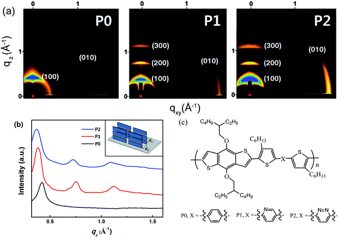 | ||
| Fig. 1 (a) 2D-GIXS images of P0, P1 and P2 films after thermal annealing; (b) out-of-plane line cuts of GIXS. Inset: schematic illustration of the edge-on orientation of the polymers with the backbone perpendicular to the substrate. The interchain lamellar spacing and the π–π stacking distances are labeled as d1 and d2, respectively. (c) Chemical structure of BDT-based D–A copolymers P0, P1 and P2 having 0, 1, or 2 nitrogen atoms in the acceptor units. Figure reprinted from ref. 25, Copyright © 2012, American Chemical Society. | ||
Many other D–A copolymers are predominantly amorphous yet exhibit weak π–π stacking in the solid state. For example, π–π stacking in the polymer PTB1 (which is based on alternating thieno[3,4-b]thiophene and benzodithiophene units) is evidenced by a ‘crescent’ observed at q = 1.71 Å−1 (d2 = 3.7 Å) in the out-of-plane direction of the 2D grazing-incidence X-ray scattering patterns, as shown in Fig. 2a.26,27 This suggests a “face-on” orientation of π–π stacking – i.e. the plane of the PTB1 backbone is oriented parallel to the underlying substrate. A diffraction ring is also observed at q = 0.23 Å−1 (d1 = 27.3 Å) that results from lamellar spacing between neighboring PTB1 backbones separated by their side-groups. The ability of conjugated polymers to preferentially π–π stack “face-on” with respect to the substrate is considered to facilitate efficient charge transport in an OPV device.27 Although PTB1 is an amorphous copolymer, the out-of-plane space-charge limited current (SCLC) charge mobility of PTB1 (∼4.5 × 10⁻⁴ cm2 V−1 s−1) is higher than that of P3HT (∼2.7 × 10⁻⁴ cm2 V−1 s−1); an effect that may well result from the fact that P3HT chains preferentially stack “edge-on” with respect to a substrate.28 When PTB1 is cast into a photovoltaic blend with PC61BM, there are negligible changes to the lamella spacing or the π–π stacking distance (see Fig. 2b and d). It can be seen however that the intensity of π–π X-ray scatter undergoes a relative reduction on mixing with PC61BM; a result explained on the basis that intermixing between the polymer and PCBM reduces long-range order within the polymer-rich phase of the film.26
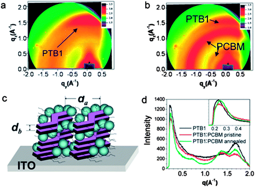 | ||
Fig. 2 GIWAXS images of (a) pure PTB1 and (b) a PTB1:PC61BM 1![[thin space (1/6-em)]](https://www.rsc.org/images/entities/char_2009.gif) :1 blend. (c) Schematic illustration of the orientation of the polymer backbone and side-chains in a PTB1:PC61BM blend. (d) X-ray intensity recorded in the out-of-plane direction of a 2D GIWAXS image. Figure reprinted from ref. 26, Copyright © 2010, American Chemical Society. :1 blend. (c) Schematic illustration of the orientation of the polymer backbone and side-chains in a PTB1:PC61BM blend. (d) X-ray intensity recorded in the out-of-plane direction of a 2D GIWAXS image. Figure reprinted from ref. 26, Copyright © 2010, American Chemical Society. | ||
Early research on the morphology of BHJ polymer:fullerene photovoltaic blends often described the nanostructure in terms of a bi-continuous network of domains, composed of sharply defined regions of pure polymer and pure-fullerene that exist as a result of spontaneous phase-separation between the components.29,30 A number of studies over the last few years have shown, however, that there are at least three phases in a polymer:fullerene photovoltaic blend; a pure polymer phase, a pure fullerene phase and a mixed phase of the two different materials.31,32 In each of the pure phases, crystalline and amorphous regions may also co-exist,33 with the extent of the crystallization dependent on the nature of molecular packing and the solution-casting process which impacts on the kinetics of molecular packing. Fig. 3 illustrates a schematic of the various different phases believed to exist in a semi-crystalline and an amorphous polymer:fullerene blend. At the molecular level, the intimately mixed phase in amorphous copolymer:fullerene blends such as PTB7 or PCDTBT with PC71BM is best described as an amorphous solid solution. Resonant Soft X-ray Scattering (R-SoXS) studies have shown that PC71BM is soluble in the mixed phase of PTB7:PC71BM blend film at a concentration of up to ∼30%.34
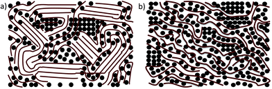 | ||
| Fig. 3 A schematic illustration of the different phases in a blend of (a) a semi-crystalline polymer and PCBM and (b) an amorphous polymer and PCBM. | ||
In some semi-crystalline copolymer:fullerene blends, X-ray scattering has revealed that fullerene molecules are able to intercalate between polymer chains.32 For example, in a pBTTT:PCBM thin-film blend, GIWAXS measurements have shown that the lamellar packing distance between pBTTT backbones increased from 21 Å (in pure pBTTT) to ∼30 Å in a 1:4 polymer:fullerene blend.32 This increase was proposed to originate from an intercalation of the fullerene molecules into the polymer crystal, forming a highly ordered bimolecular crystal. Although molecular mixing of fullerenes may in principle disrupt the packing of an amorphous polymer, such effects are often difficult to confirm using X-ray diffraction techniques alone due to the low level of polymer crystallinity.35 The influence of fullerene derivative structure on the morphology and photovoltaic performance of copolymer:fullerene blend films will be discussed in detail later in this Review.
Recent studies have identified the importance of the intermixed phases of PCBM and polymer on the optoelectronic processes of solar cells.36,37 These finely mixed polymer/fullerene phases are believed to improve the yield of free charge carriers within a BHJ film. In addition, the formation of appropriately sized percolating pure phases permits the relatively efficient transport of charge carriers towards the solar cell electrodes.36,37 For high performance solar cells, it is desirable that the intermixed phase co-exists with the relatively pure phases, rather than the formation of a one-phase system comprised of a solid solution.37
3. The impact of molecular structure of D–A copolymers on energy level, band-gap, charge mobility, molecular packing and photovoltaic device performance
3.1 Effects of donor and acceptor moiety
Upon photoexcitation of a conjugated polymer, a minimum energy offset between the LUMO level of the polymer donor and the PCBM acceptor of approximately 0.3 eV has often been deemed necessary to efficiently drive electron transfer to the fullerene.38,39 For example, taking PC61BM as the acceptor (having a LUMO level at −4.2 eV), this implies a minimum LUMO level of the polymer donor of −3.9 eV is necessary to permit charge transfer to the PC61BM (Fig. 4).5,7 In a photovoltaic device, a deeper HOMO level of the polymer donor will help increase the device Voc; a concept confirmed by a statistical review.7 However, Voc is reduced when the HOMO level is lower (i.e. closer to vacuum) than −5.7 eV.7 As PC61BM has a low extinction coefficient at visible and near-IR wavelengths, the polymer donor is the main light-absorbing component in a photovoltaic blend. The same statistical summary shows that reducing the D–A copolymer bandgap results in a higher Jsc as more of the sun's radiation can be harvested. However, once the bandgap falls below 1.3 eV, the Jsc starts to fall.7 It appears therefore that a bandgap of 1.4 to 1.5 eV is ideal for efficient sunlight absorption and subsequent photocurrent generation. Consequently, in BHJ thin-films using PC61BM as an electron acceptor the optimum HOMO level of the polymer should be around −5.4 eV.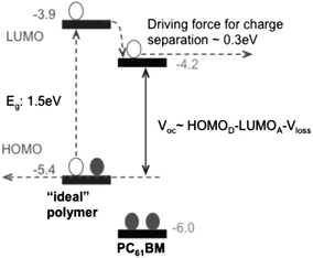 | ||
| Fig. 4 Schematic energy level alignments between an “ideal polymer” donor and a PC61BM acceptor. | ||
For D–A copolymers, the energies of the molecular orbital levels and the corresponding band-gap are primarily determined by the chemical and structural composition of the conjugated backbone, with the HOMO (LUMO) level generally determined by that of the electron donating (accepting) moiety.40 This architecture permits the HOMO and LUMO levels of the copolymer to be defined almost independently of one other. Note however that the size, structure and position of solubilising side-groups on the co-polymer backbone also provide an opportunity to fine-tune the position of these energy levels. A large number of D–A copolymers have been synthesized by employing different electron-rich and electron-deficient moieties along the backbone and by rational control over side-chains, bridging units and substituents along the repeating units of a D–A conjugated copolymer.5–9 Examples of donor and acceptor moieties are shown in Fig. 5. Here, electron-rich heterocycles such as fluorene, carbazole, cyclopentadithiophene (CPD), naphtho[2,1-b:3,4-b′]-dithiophene (NDT), benzo[1,2-b:4,5-b′]dithiophene (BDT), dithieno[3,2-f:2′,3′-h]quinoxaline (QDT), thiophene-phenylene-thiophene (TPT) dithieno[3,2-b:2′,3′-d]-silole (DTS) indacenodithiophene (IDT) have been used as the donor moieties, with electron-deficient heterocycles such as 2,1,3-benzothiadiazole (BT), 4,7-di-2-thienyl-2,1,3-benzothiadiazole (DTBT), diketopyrrolopyrrole (DPP), thiadiazolo[3,4-c]pyridine (PyT), thieno[3,4-c]pyrrole-4,6-dione (TPD), dithieno[3,2-f:2′,3′-h]quinoxaline (DTQ) employed as the acceptor. Synthesizing D–A copolymers with characteristically “weak donor” and “strong acceptor” moieties has been demonstrated to create semiconductors having relatively deep HOMO levels and narrow band-gaps.7 Here, the “weak donor” reduces the D–A polymer HOMO level whilst the “strong acceptor” reduces the energy band-gap via intra-molecular charge transfer (ICT) behavior.7 We refer the interested reader to the literature for an empirical comparison of the electron donating ability of various donor units, as well as examples of strong acceptors.7
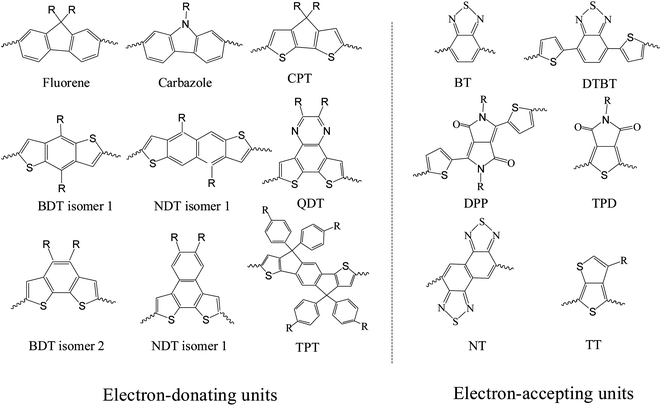 | ||
| Fig. 5 Chemical structures of selected electron-donating and electron-accepting units used in D–A copolymers. | ||
It is important to acknowledge that the use of a copolymer:PCBM blend having (in theory) ‘ideal’ HOMO and LUMO levels may not necessarily translate into a high-performance OPV device. Recombination of charge carriers, either via germinate or non-germinate processes, will act to reduce the maximum achievable Voc and Jsc of a device. Such effects can in principle be influenced by the presence of non-ideal active layer morphology. Practically therefore, an ideal polymer should also exhibit favourable miscibility and undergo phase separation at appropriate length-scales with an electron acceptor. It should also have a high and balanced charge carrier mobility (i.e. comparable to charge transport between fullerene molecules) in a BHJ blend thin-film. Furthermore, in order to minimize oxidation of the copolymer, the HOMO level should also be sufficient deep (≤−5.27 eV) to ensure operational stability of a working OPV device. Such requirements for fabricating an efficient OPV device indicate the existence of a highly complex ‘parameter-space’ in which many different co-polymers can be conceived. In the following sections we examine these effects in a number of different copolymer families.
3.2 Effects of side-chain distribution and structure
The addition of side chains to a co-polymer backbone – either grafted onto the donor and/or the acceptor moieties – will influence its physical properties such as solubility and propensity to undergo self-organization. Side-chains will also modify the electronic (electrochemical) properties of the copolymer which – when blended with an electron acceptor in a BHJ thin-film – will consequently affect the optoelectronic properties of the resultant device.41–43 During the design and synthesis of a new copolymer, the choice of side-chains becomes an important consideration as it is necessary to optimise solubility (and therefore processability) with optoelectronic properties of the resultant semiconductor.The length and shape of the side-chains in the D–A copolymer PDTSTPDs have been found to affect the self-assembly and packing of the polymer in photovoltaic blend thin-films.44 Indeed by increasing the length of alkyl chains attached to the TPD unit of copolymer PDTSTPD, it was possible to improve material solubility and facilitate the formation of lamellar structures within a blend thin-film.44 When blended with PC71BM in an BHJ thin-film, this structural characteristic of PDTSTPD permitted the fabrication of OPV devices having a relatively high power conversion efficiency (PCE) of 7.5%.44 In other studies, the effect of butyl (Bu), hexyl (He), octyl (Oc), and 2-ethylhexyl (EH) alkyl side chains were examined in D–A copolymers composed of TPD and benzodithiophene (BDT) units.45 It was shown that alkyl chains on the TPD unit had a significant influence on the solubility and chain packing of the polymer, in addition to providing a ‘fine-tuning’ of molecular orbital levels. X-ray scattering revealed that the π–π stacking distance is around 3.67 Å in PCPDTTPD (see molecular structure in Fig. 6) polymers having linear side-chains (Bu, He and Oc), whilst for the EH branched copolymers, the π–π stacks were separated by 3.86 Å (Table 1), indicating a lower packing density. Copolymers PCPDTTPD-Oc and PCPDTTPD-EH with Oc or EH groups had lower HOMO and LUMO energy levels, resulting in a relatively higher Voc in OPV devices when blended with PC71BM, permitting PCEs of up to 6.4% to be obtained in devices based on a PCPDTTPD-Oc:PC71BM blend.45 These findings are in qualitative agreement with a similar study on the furan-containing copolymer PDPP2FT (see molecular structure in Fig. 6), where it was found that linear branched chains permitted the formation of larger and closer packed nanoscale crystallites, compared to those formed from an almost identical polymer that instead incorporated branched EH chains (Table 2).46 It is known that the degree of electronic coupling between adjacent polymer chains decays exponentially with π–π stacking distance and can vary by as much as a factor of 4 as this distance is increased from 3.4 to 4.0 Å.46 Thus branched side groups may introduce steric hindrance if polymer chains undergo packing, whereas linear side groups may result in a relatively coplanar backbone structure thereby allowing for closer π–π stacking distances and consequently enhanced charge mobility. By understanding and utilizing such effects, it is possible to obtain substantial increases in OPV PCE.
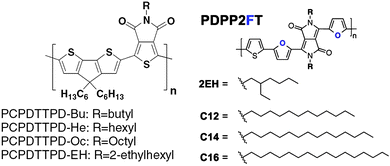 | ||
| Fig. 6 The chemical structure of PCPDTTPD and PDPP2FT with various side chains. | ||
| Polymer | HOMO (eV) | LUMO (eV) | π–π stacking distance (Å) | Eoptg (eV) | Voc (V) | Jsc (mA cm−2) | FF (%) | PCE (%) |
|---|---|---|---|---|---|---|---|---|
| PCPDTTPD-Bu | −5.08 | −3.43 | 3.67 | 1.57 | 0.70 | 9.22 | 35.7 | 2.3 |
| PCPDTTPD-He | −5.12 | −3.47 | 3.67 | 1.59 | 0.75 | 13.2 | 57.4 | 5.7 |
| PCPDTTPD-Oc | −5.29 | −3.63 | 3.67 | 1.59 | 0.75 | 14.1 | 60.7 | 6.41 |
| PCPDTTPD-EH | −5.24 | −3.55 | 3.86 | 1.61 | 0.84 | 12.7 | 53.5 | 5.71 |
Interestingly however, a contrasting effect was found in PBDTTPD-based OPV devices.47 Here GIXS was used to study the copolymer PBDTTPD having either two branched EH side-chains (2EH, C8) or linear side-chains (C8, C14) on a BDT moiety. From the scattering patterns shown in Fig. 7, it can be seen that the copolymer PBDTTPD having the branched side-chains adopts a preferential “face-on” π–π stacking orientation whilst the equivalent polymer with linear side-chains does not show any preferential π–π stacking orientation when processed under identical conditions. This apparent selectivity results in a dramatic improvement in device PCE from 4.1% to 7.5% when linear side-chains were replaced with branched side-chains.
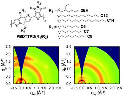 | ||
| Fig. 7 Top: chemical structure of PBDTTPD with different side-chains on the BDT or TPD units. Bottom: 2D GIXS patterns of (left) PBDTTPD (2EH/C8) and (right) PBDTTPD (C14/C8) in optimized BHJs with PC71BM. Figure reprinted from ref. 47, Copyright © 2013, American Chemical Society. | ||
| Polymers | π–π stacking distance (Å) | π–π stacking correlation length (nm) | L (Å) | Lamellar correlation length (nm) | Avg. PCE (%) |
|---|---|---|---|---|---|
| PDPP2FT-C12 | 3.6 | 3.3 | 21 | 3.4 | 4.8 |
| PDPP2FT-C14 | 3.6 | 3.6 | 23 | 3.6 | 6.2 |
| PDPP2FT-C16 | 3.6 | 3.0 | 25 | 4.1 | 5.7 |
| PDPP2FT-2EH | 3.7 | 1.1 | 13 | 2.7 | 5.0 |
Within the PTB series of copolymers synthesized with either thienothiophene (TT) or benzodithiophene (BDT) moieties, a range of PCEs have been determined ranging from 2 to 8% dependent on the nature of the side-chain.48 It was shown using GIWAXS that branched side-chains attached to the BDT unit increased the π–π stacking distance in the solid film and reduced the performance of the OPV device.48 However, the addition of branched side-chains to the TT unit did not have a significant impact on the π–π stacking distance. Here, the performance of devices incorporating copolymers containing TT unit with branched alkyl side-chains was substantially higher, with such differences tentatively ascribed to favorable interactions with the PCBM component of the blend. An empirical correlation between π–π stacking distance and the fill factor of PTB copolymer-based OPV devices was also demonstrated, with a reduced π–π stacking distance in the polymer phase correlated with a larger FF in OPV devices.
The length of the alkyl side-chains was not found to significantly influence the absorption spectrum or molecular orbital levels in D–A copolymer PBDTTBTs.49 Nevertheless, the nanoscale morphology of polymer:PCBM blend thin-films can be dramatically altered. Transmission Electron Microscopy (TEM) images shown in Fig. 8 reveal that increasing the length of the alkyl side-chains can directly modify the morphology of the blend.49 Specifically, it was found that shorter side chains gave rise to a BHJ morphology, containing fullerene aggregates described by the authors as being ‘pea-like’, whereas blends of a fullerene and polymer having longer side chains formed a relatively coarse interpenetrating network characterized by larger phase separation between the components. Despite such variations in BHJ nanostructure, X-ray scattering measurements did not indicate any differences in the polymer π–π stacking distance. The changes in blend morphology were consequently attributed to variations in miscibility between the different polymers and PCBM.
 | ||
| Fig. 8 TEM images of blend films spin-coated from chlorobenzene for (a) PBDTTBT/PC61BM (w/w, 1:3); (b) PBDTBTC6/PC61BM (w/w, 1:3); (c) PBDTTBT-C8/PC61BM (w/w, 1:3); (d) PBDTTBT-C10/PC61BM (w/w, 1:3); and (e) PBDTTBT-C12/PC61BM(w/w, 1:3). Figure reprinted from ref. 49, Copyright © 2011, American Chemical Society. | ||
The addition of conjugated side-chains to the backbone structure of D–A copolymers has also been explored, resulting in a two-dimensional (2D) conjugated system. Huo et al. reported a study of the 2D D–A copolymers PBDTTBT, PBDTTTZ created by attaching conjugated thienyl or 2-alkylthiophene side-chains to the electron-donating BDT units.50,51 Such materials were blended with PC71BM and used as the active layer in an OPV having a PCE in excess of 5%.50,51 A 2D BDT-based D–A copolymer named PBDTDTNT has also been shown to achieve a PCE of 6% when fabricated into an OPV.52 In D–A copolymers based on BDT and TT units (see chemical structures shown in Fig. 9), the 2D D–A copolymers PBDTTT-E-T, PBDTTT-C-T and PBDTTT-S-T having conjugated side-chains exhibited better thermal stability, red-shifted absorption, lower HOMO and LUMO energy levels, significantly higher hole mobility and greatly improved photovoltaic properties in comparison to their corresponding alkoxy-substituted analogues (i.e. having insulating side groups) PBDTTT-E, PBDTTT-C and PBDTTT-S.53,54 We summarize device and material properties taken from ref. 53 and 54 in Table 3.
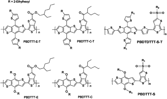 | ||
| Fig. 9 Chemical structures of PBDTTT-E, PBDTTT-C, PBDTTT-S and their 2D D–A copolymer analogues PBDTTT-E-T, PBDTTT-C-T, PBDTTT-S-T. | ||
| Polymer | HOMO (eV) | LUMO (eV) | Eoptg (eV) | SCLC mobility (cm−2 V−1 s−1) | Voc (V) | Jsc (mA cm−2) | FF (%) | PCE (%) |
|---|---|---|---|---|---|---|---|---|
| PBDTTT-E | −5.04 | −3.19 | 1.63 | 1.50 × 10⁻³ | 0.66 | 11.53 | 54.7 | 4.16 |
| PBDTTT-E-T | −5.09 | −3.22 | 1.58 | 6.74 × 10⁻³ | 0.68 | 14.59 | 62.6 | 6.21 |
| PBDTTT-C | −5.07 | −3.21 | 1.60 | 5.53 × 10⁻⁴ | 0.70 | 15.51 | 59.2 | 6.43 |
| PBDTTT-C-T | −5.11 | −3.25 | 1.58 | 2.7 × 10⁻¹ | 0.74 | 17.48 | 58.7 | 7.59 |
| PBDTTT-S | −5.10 | −3.51 | 1.65 | 4.56 × 10⁻⁴ | 0.76 | 13.85 | 58.0 | 6.11 |
| PBDTTT-S-T | −5.04 | −3.57 | 1.59 | 2.76 × 10⁻³ | 0.69 | 16.35 | 66.3 | 7.48 |
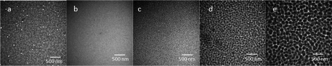
The positions at which solubilising side-chains are attached to the repeat units of a copolymer has also been found to influence its physical and optoelectronic properties and consequently device performance.55,56 If significant steric hindrance is introduced by the side-chains, the maximum molecular weight of the copolymer that can be achieved through polymerization is however significantly reduced.57 The inappropriate positioning of side-chains can also result in twists along the conjugated backbone with such effects leading to a reduction in effective conjugation length and charge carrier mobility.58 For example in some D–A copolymers, it was found that side-chains attached at the 4-position of a thiophene ring result in less steric hindrance and consequently form more planar molecular structures.59,60 In another study on two phenazine-based D–A copolymers, (see chemical structures shown in Fig. 10) it was found that film morphology and photovoltaic performances were dependent on the position of alkoxy chains on the phenazine unit, although the optical absorption and energy levels were not apparently affected by side-chain position.61 From the AFM and TEM morphologies shown in Fig. 10 it can be seen that large, coarse aggregates are formed in P1/PC71BM blend film (with OPV devices having a PCE of 1.5%), whereas a P2/PC71BM blend formed a homogeneous and smooth film, producing devices having a PCE of 2.54%.61
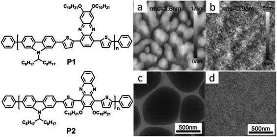 | ||
| Fig. 10 Left: chemical structures of two phenazine-based D–A copolymers. Right: (a) AFM and (c) TEM images of P1/PC71BM (1:3, w/w), and (b) AFM and (d) TEM images of P2/PC71BM (1:3, w/w) blend films. AFM images are 2 μm × 2 μm. The scale bar in TEM images is 500 nm. Figure reprinted from ref. 61, Copyright © 2013 Wiley Periodicals, Inc. | ||
3.3 Effects of bridging units
The bridging units that exist between the donor and acceptor moieties of D–A copolymers have been found to affect the light absorption, energetic band-gap and charge-carrier mobility of the copolymer and thus consequently affect OPV device power conversion efficiency. Bridging units can also affect material solubility. For example the replacement of thiophene with furan heterocycles along the backbone of D–A copolymers enables the use of relative short side chains owing to the improved solubility of furan in common organic solvents.62 In other studies, the length of the π-conjugated bridge between D and A groups was found to affect the electronic and photovoltaic properties of copolymers based on carbazole and quinoxalinoporphyrin.63 By increasing the length of the π-conjugated bridge from thiophene to bithiophene and then to terthiophene, the hole mobility of the copolymers increased gradually and the optical absorption spectra broadened.63 These effects were correlated with an improved PCE in a solar cell device utilizing these semiconductors. In other work on copolymers based on a BDT (benzodithiophene) donor unit and a BT (benzothiadiazole) acceptor unit, the choice of π-bridging unit was found to significantly affect both the molecular architecture and the optoelectronic properties of the polymer.64 A series of representative polymers is shown in Fig. 11. It was found that when the π-bridge was varied from furan to thiophene, and then to thienothiophene, the absorption spectrum of the polymer underwent a relative red-shift. Furthermore, the conformation of the copolymer repeat unit (as inferred from Density Functional Theory (DFT) calculations) changed from a ‘zig-zag’ arrangement to one in which the repeat unit was relatively linear.64 Such structural and optoelectronic changes were correlated with improved charge carrier mobility and OPV device performance (Table 4). It was concluded therefore that a thienothiophene bridge conferred significant advantages in this class of OPV-applicable D–A copolymer.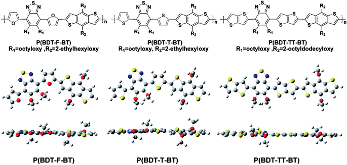 | ||
| Fig. 11 Molecular structures of BDT and BT based D–A copolymers with different π-bridges, along with optimized geometries of backbone of copolymers obtained from density functional theory calculation. Color code: gray (C), white (H), red (O), blue (N), and yellow (S). Figure reprinted from ref. 64, Copyright © 2012 American Chemical Society. | ||
Selenium atoms are more electron-rich than sulfur atoms and aromatic rings containing selenium have electrons that are consequently more delocalised compared to their thiophene counterparts.65–67 D–A copolymers bridged by selenophene units have been found to exhibit red-shifted absorption spectra and lower optical band-gaps compared to identical copolymers bridged by thiophene units.65–67 Several selenophene containing polymers have also demonstrated enhanced charge-carrier mobility compared with thiophene-based polymers.68–71 For example, a PCE of 7.2% was obtained in single-junction OPV devices based on selenophene-bridged PBDTTSeDPP, compared with the furan-bridged polymer PBDTT-FDPP and thiophene-bridged PBDTT-DPP (PCEs of 4.7 and 6.5 respectively).72 In contrast however, reduced field-effect charge mobility and reduced PCE have been found in selenophene-bridged copolymers comprising 2,7-linked carbazole or fluorene donor moieties and benzothiadiazole units with or without alkoxy substituents as acceptor moieties (see chemical structures in Fig. 12).73 Device studies indicate that relative to thiophene-containing copolymers, selenophene-bridged copolymers are characterized by OPVs having higher Jsc but smaller Voc and FF,66,73 or exhibit both a reduced Jsc and FF.73 In this series of copolymers, the reduced efficiency of OPVs containing selenium substituted materials was attributed to lower charge carrier mobility and reduced molar extinction coefficient that limited the ability of the copolymer to harvest light and transport charge efficiently though the device.73
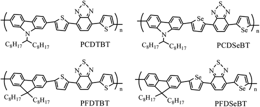 | ||
| Fig. 12 Chemical structures of thiophene- and selenophene-bridged D–A copolymers PCDTBT, PCDSeBT, PFDTBT and PFDSeBT. | ||
| Polymer | Blend ratio | Voc (V) | Jsc (mA cm−2) | FF (%) | PCE (%) | SCLC mobility (cm−2 V−1 s−1) |
|---|---|---|---|---|---|---|
| P(BDT-F-BT) | 1:2 | 0.94 | 6.50 | 46 | 2.81 | 2.1 × 10⁻³ |
| P(BDT-T-BT) | 1:1.5 | 0.82 | 9.45 | 48 | 3.72 | 2.9 × 10⁻³ |
| P(BDT-TT-BT) | 1:1.5 | 0.69 | 11.34 | 63 | 4.93 | 8.6 × 10⁻³ |
The bridging atoms in the donor or acceptor moieties of the copolymers have also been shown to significantly influence the nanostructure of polymer and polymer:fullerene blend thin-films.74,75 For example, the carbon-bridged dithiophene-based copolymer PCPDTBT (see Fig. 13) is typically amorphous when cast into a solid film. In contrast its silicon-bridged analog PSBTBT is semi-crystalline76,77 with GIWAXS demonstrating a preferential ‘edge-on’ orientation of molecular chains, with the π–π stacking plane parallel to the substrate.76 It was suggested that the longer C–Si bond in PSBTBT permitted better inter-chain molecular packing due to reduced steric hindrance between the alkyl side-group and the thiophene rings. As PSBTBT is a semi-crystalline polymer, its hole-carrier mobility (as determined by field effect transistor measurements) is approximately 3 times higher than that of the relatively amorphous polymer PCPDTBT.78 Nevertheless, an optimized device PCE of around 5.5% was achieved in OPVs made from both PCPDTBT or PSBTBT copolymers, although it is important to acknowledge that optimization was achieved via the use of solvent additives79 and post-deposition thermal annealing76,78 respectively. These different optimization protocols highlight the complexity in OPV research by demonstrating that polymers with apparently unfavourable OPV characteristics (for example, an amorphous nature and relatively low charge mobility) can still be used to create devices with relatively high PCEs.
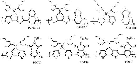 | ||
| Fig. 13 Chemical structures of PCPDTBT, PSBTBT, PGe1-EH, PDTC, PDTSi and PDTP. | ||
In the germanium-bridged derivative of PCPDTBT – named PGe1-EH (see Fig. 13), it was found that OPV devices had a low PCE of 2.9%.80 It is clear that a C–Ge bond is longer than that of a C–Si bond, however the impact of this difference on molecular packing in PGe1-EH and its relationship with the photovoltaic performance has not yet been determined. In other work, it was found that the Ge-bridged copolymer with methyl side groups (MeGeBT) had a higher hole-carrier mobility and improved miscibility with PC71BM; properties that lead to the realization of OPVs having a higher PCE compared to devices fabricated using the Si-bridged copolymer MeSiBT.81 Other OPV device studies using copolymers containing electron-deficient thienopyrroledione (TPD) and electron-rich dithiophene units bridged by carbon, silicon and nitrogen atoms (namely PDTC, PDTSi and PDTP, respectively – see Fig. 13) demonstrated a reduction in PCE when the dithiophene units were Si- and N-bridged (Table 5).82 Although the PCE of OPVs fabricated using PDTSi and PDTP can be improved slightly by casting from different solvents, the resultant PCEs are still lower than that of devices made from PDTC. It was concluded therefore that the use of Si- and N-bridges did not present an effective strategy to increase OPV efficiency using this class of D–A copolymers. Finally, Wu et al. developed an sp2–sp2 ethylene (C![[double bond, length as m-dash]](https://www.rsc.org/images/entities/char_e001.gif) C) bridged dithienocarbazole-based D–A copolymer called PDTBCDTBT. The PCE of OPVs based on this copolymer reached 6.2%; an efficiency amongst the highest of those obtained from C-, Si- and N-bridged analogous copolymers.83
C) bridged dithienocarbazole-based D–A copolymer called PDTBCDTBT. The PCE of OPVs based on this copolymer reached 6.2%; an efficiency amongst the highest of those obtained from C-, Si- and N-bridged analogous copolymers.83
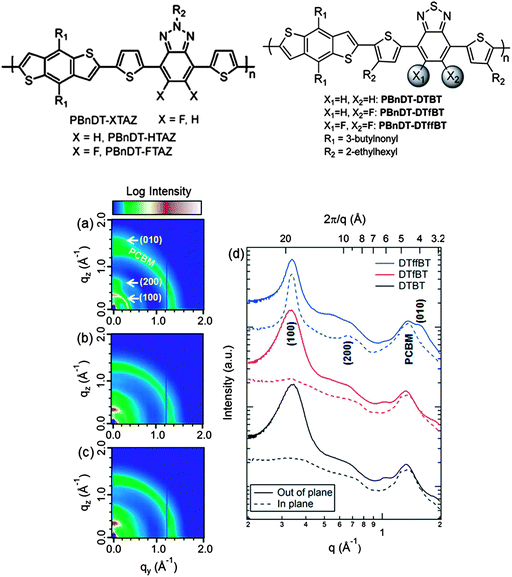 | ||
| Fig. 14 Top: chemical structures of PBnDT-HTAZ, PBnDT-FTAZ, PBnDT-DTBT, PBnDT-DTfBT, and PBnDT-DTffBT. Bottom: 2D GIWAXS images of blend films based on (a) PBnDT-DTffBT, (b) PBnDT-DTfBT, and (c) PBnDT-DTBT. (d) In-plane and out-of-plane 20° sectors with the polymer peaks labeled along with the typical scattering contribution from PC61BM. Figure reprinted from ref. 96, Copyright © 2013, American Chemical Society. | ||
3.4 Effects of fluorine substitution
Substitution of carbon or hydrogen atoms with fluorine in either the donor or acceptor unit of a D–A copolymer has been shown to modify the molecular orbital levels of a copolymer, and subsequently impact upon the photovoltaic performance of an OPV device.84–87 Fluorination of D–A copolymers can simultaneously lower the HOMO and LUMO energy levels, causing only minor changes to the optical band-gap.88,89 Consequently, reduced energy-loss on electron transfer from the polymer donor to fullerene acceptor (via reduction of the LUMO level) and enhanced stability against photo-oxidation (by lowering the HOMO level) can be achieved, with such changes predicted to increase the efficiency and operational lifetime of organic electronic devices.90 Furthermore, C–F⋯H, F⋯F and C–F⋯πF atomic interactions can also improve molecular organization resulting in shorter π–π stacking distances that enhance charge carrier mobility.91 Fluorination is therefore a promising approach to improving the PCE of OPV devices by increasing the Voc, Jsc and FF either monotonically92,93 or simultaneously.89,94 For example, in OPV devices utilizing the fluorinated copolymer F-PCPDTBT (otherwise equivalent to PCPDTBT as shown in Fig. 13, with the exception of a fluorine atom attached on the BT unit), power conversion efficiencies of up to 6% were achieved; a value greater than the 3.6% determined from non-fluorinated PCPDTBT-based solar cells that were processed under identical conditions.95 Indeed, time-delayed charge extraction measurements determined a relatively low yield of both geminate and non-geminate charge recombination in solar cell devices using F-PCPDTBT in comparison with the non-fluorinated PCPDTBT.95| polymer | HOMO (eV) | LUMO (eV) | Eg (eV) | Eoptg (eV) | Voc (V) | Jsc (mA cm−2) | FF (%) | PCE (%) |
|---|---|---|---|---|---|---|---|---|
| PDTC | −5.43 | −3.25 | 2.18 | 1.67 | 0.80 | 10.04 | 47 | 3.7 |
| PDTSi | −5.44 | −3.17 | 2.27 | 1.70 | 0.91 | 2.32 | 56 | 1.18 |
| PDTP | −5.16 | −3.08 | 2.08 | 1.59 | 0.71 | 2.53 | 50 | 0.91 |
In other work, You et al. introduced two fluorine atoms to the benzotriazole and benzothiadiazol unit, and synthesized the fluorinated D–A copolymers PBnDT-FTAZ89 and PBnDT-DTffBT94 whose chemical structures are shown in Fig. 14. Both of these materials (when blended with PC61BM) were used to create OPV devices having a relatively high PCE of over 7%. Due to the high hole mobility of PBnDT-FTAZ, it was shown that a relatively-high PCE of 6% could be realized for PBnDT-FTAZ:PC61BM OPV devices in which the active layer thickness exceeded 1 μm. A follow-on study96 on the impact of the number of fluorine atom substitutions per monomer group (0, 1 or 2, as shown in the chemical structures in Fig. 14) attributed the relatively larger Voc obtained in OPV devices based on such materials to a lowering of the HOMO level of the fluorinated copolymer (see a summary of HOMO levels in Table 6), with improvements in Jsc and FF tentatively ascribed to reduced charge recombination within the photoactive layer. Measurements on OPV devices under a range of light intensities also confirmed a reduced bimolecular recombination rate with increased fluorine concentration.96 GIWAXS measurements of neat films of the doubly fluorinated copolymer PBnDT-DTffBT revealed an increase in X-ray scattering intensity compared to its single and non-fluorinated analogues from both the in-plane lamellar packing and out-of-plane π–π stacking. These results were consistent with miscibility measurements of the fluorinated polymers and PC61BM using resonant soft X-ray scattering measurements (R-SoXS).96 Here, it was shown that the miscibility of PC61BM with the non-fluorinated polymer PBnDT-DTBT was greater than in the fluorinated analogue PBnDT-DTffBT (being 21% and 12% by weight respectively). This resulted in the formation of larger polymer and fullerene domains having relatively higher purity in the PBnDT-DTffBT:PC61BM blend.
| Polymer | HOMO (eV) | LUMO (eV) | Eoptg (eV) | SCLC mobility (cm−2 V−1 s−1) | Voc (V) | Jsc (mA cm−2) | FF (%) | PCE (%) |
|---|---|---|---|---|---|---|---|---|
| PBnDT-HTAZ | −5.29 | −2.87 | 1.98 | 3.34 × 10⁻⁶ | 0.71 | 11.28 | 54.5 | 4.3 |
| PBnDT-FTAZ | −5.36 | −3.05 | 2.00 | 6.76 × 10⁻⁵ | 0.79 | 12.45 | 72.2 | 7.1 |
| PBnDT-DTBT | −5.40 | −3.13 | 1.70 | n/a | 0.87 | 10.03 | 57.3 | 5.0 |
| PBnDT-DTffBT | −5.54 | −3.33 | 1.70 | n/a | 0.91 | 12.91 | 61.2 | 7.2 |
Incorporation of fluorine into various positions on polythienothiophene-co-benzodithiophenes (PTBF) copolymers has been found to change device efficiency between 2.3% and 7.2%.97 In all cases, the energy band-gap of the copolymer was increased after fluorination. It was shown that PTBF copolymers containing mono-fluorinated thienothiophene units resulted in the best solar cell performance.97 Perfluorination of the polymer backbone led to poor compatibility with PC71BM and consequently reduced photovoltaic performance. As shown in Fig. 15, polymer:fullerene blends made from PTBF0 and PTBF1 and PC71BM were characterized by relatively fine features, which are typical for nanoscale phase separation. In contrast, larger PC71BM domains ranging in size from 50 to 200 nm were found to exist in blend thin-films of PTBF2 and PTBF3, suggesting relatively large-scale phase separation.97 This difference in morphology was attributed to the fluorophobicity of PC71BM molecules and the enhanced self-organization ability of perfluorinated polymer chains. The strong driving force for the development of relatively long-range order is partly driven by the planarity of the polymer backbone; a property that favors the exclusion of fullerene molecules and induces phase separation in the blends. Such physical properties however come at a price; it was shown that perfluorination of the polymer backbone resulted in poor stability against attack by singlet oxygen.
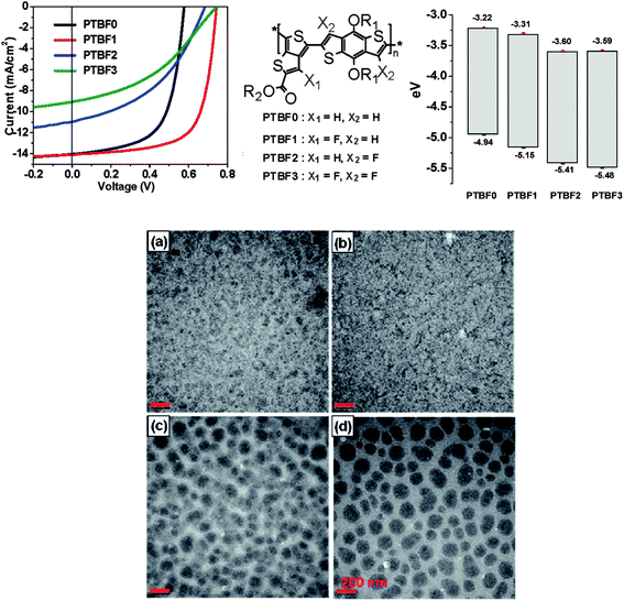 | ||
| Fig. 15 Top: device performance, chemical structure and energy levels of various PTBF polymers. Bottom: TEM images of polymer/PC71BM blend films prepared from a DCB solvent: PTBF0 (a), PTBF1 (b), PTBF2 (c), and PTBF3 (d). Scale bar = 200 nm. Figure reprinted from ref. 97, Copyright © 2011, American Chemical Society. | ||
4. The impact of fullerene size and side-group structure on molecular mixing and photovoltaic device performance
The choice of electron-acceptor in OPV studies has often focused on the use of PC61BM or PC71BM, with the latter exhibiting enhanced optical absorption at visible wavelengths. Nevertheless, a number of other fullerene derivatives having additional or alternative side-groups compared to PCBM (see Fig. 16) have attracted attention as potential high-performance electron acceptors.98–103 Critically, such fullerene derivatives may not necessarily behave as ‘universal’ good electron-acceptors in BHJ OPVs as variations in fullerene molecular structure affect not only electron affinity, but also the ability of the molecule to self-organize and mix with the electron-donating polymer.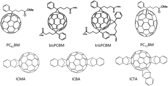 | ||
| Fig. 16 Molecular structures of a few different types of fullerene derivative. | ||
In comparison to mono-PCBM, higher adduct versions of PCBM, namely bis-PCBM and tris-PCBM, exhibit LUMO levels closer to vacuum.98,99 Ideally, such changes result in a reduction in energetic losses associated with electron transfer between polymer and fullerene and in principle provide an alternative approach to increase the Voc in a polymer:fullerene OPV. Indeed, it was found that device Voc increased by 0.15 V (from 0.58 to 0.73 V) when the electron acceptor was changed from PCBM to bis-PCBM in a P3HT-based OPV.98 This increase resulted in an overall improvement in PCE as both the device Jsc and FF were relatively unchanged upon fullerene substitution. Note however, that bis-PCBM needs additional purification in order to remove traces of alternative adducts that poorly define the LUMO level of the fullerene mixture or otherwise cause charge traps.98,99 It has been shown that tris-PCBM has a LUMO level closer to vacuum than either mono- or bis-PCBM and when used in an OPV device, and (using P3HT as the electron donor) a relatively high Voc can be obtained.104 However the FF and Jsc of such devices are significantly reduced, resulting in very low PCEs. Detailed studies of the photo-physics, charge transport properties and blend morphology have been used to provide key insight into such device results.104,105 Although the yield of free charges (as probed using transient absorption spectroscopy) is comparable for all P3HT:fullerene blends, higher-adduct fullerenes have been found to have progressively reduced electron mobility compared to PCBM. This can be partly explained by the relatively amorphous nature of higher-adduct fullerenes that inhibit the ability of the molecules to aggregate and form percolated electron transporting networks when cast into a BHJ blend. Furthermore, differences in relative crystallinity of the multi-adduct fullerenes also affect both the nanostructure of the polymer phase of a blend film and the ability of the fullerene to dissolve in the amorphous polymer phase.
A promising alterative to PCBM is the fullerene derivative ICMA and its higher adducts ICBA and ICTA (having two and three side-groups respectively).100,106 In qualitative agreement with studies on P3HT:bis-PCBM, P3HT:ICBA solar cells have a Voc of up to 0.84 V – an open-circuit voltage that is one of the highest obtained to date for BHJ OPV devices employing P3HT as the electron donor.107 This resulted in a PCE of up to 6.5% in a P3HT:ICBA device, an observation demonstrating that a high Voc can be obtained without causing a significant reduction in Jsc or FF.107 ICBA has also been found to improve device PCE by 50% compared to PCBM when blended with the thiazolothiazole–dithienosilole based donor–acceptor copolymers PSEHTT, PSOTT and PSOxTT.108 The application of ICTA as electron acceptor in P3HT based OPV devices does not however produce efficient photovoltaic performance, with PCE values limited to 2.5%.106 Here, the reduced electron mobility of ICTA has been proposed as the dominant factor for low device performance,106 with the presence of multiple side-groups increasing the separation between C60 moieties and consequently reducing the efficiency of electron transfer.109
Other studies on OPV devices using either Si-PCPDTBT or PFODTBT as electron donor and ICMA as electron acceptor have demonstrated a lower PCE compared to devices using PCBM as the electron acceptor.110 Even lower PCEs have been determined in devices incorporating higher adduct derivatives of ICMA. This trend can be linked to a progressively smaller energetic offset between the LUMO levels of the copolymer and the fullerene. Work by Faist et al.110 has empirically determined a minimum energetic offset between LUMO levels in these blend systems below which photoluminescence quenching is reduced and charge transfer is effectively ‘switched off’. Note that the photocurrent generation step precedes the transport of free charge carriers though the BHJ blend; a process that may also be inefficient owing to the relatively low electron mobility of ICBA and ICTA. Other work on OPV devices utilizing a blend of PSPDTTBT and ICBA have demonstrated higher PCEs compared to devices incorporating PCBM as the electron acceptor.111 Although PCBM has been shown to have a significantly higher field-effect electron mobility than ICBA when prepared in a pure film, the electron and hole mobility were found to be more balanced in an ICBA blend film (as determined in a space-charge limited conduction regime). This observation was correlated with the higher photovoltaic performance of a PSPDTTBT:ICBA blend. This result was further explained on the basis of contact angle measurements that characterized the surface energy (γ) of PSPDTTBT, ICBA and PCBM.111 Here, the largest difference in surface energies (Δγ) was determined between PSPDTTBT and ICBA; a property that is believed to provide the driving force to create a more phase-separated mixture of polymer and fullerene, facilitating the formation of semi-crystalline polymer phases. Variations in Δγ and the substrate surface energy also provide a driving force for vertical stratification in the blend; a process that may also result in the formation of a favourable BHJ morphology having improved OPV device efficiency.111
Morphological studies on BHJ blends comprising various polymers with indene C60 bis-adducts have provided additional insight into the necessary design rules that help predict whether a polymer:fullerene blend will perform well when fabricated into an OPV device.112–114 For example the polymer PBTTT is a relatively crystalline polymer having adjacent side-groups that are positioned sufficiently far apart such they can potentially permit the molecular intercalation of fullerene molecules. To explore this process, PBTTT:fullerene blends have been characterized using X-ray diffraction techniques to determine the extent of bimolecular packing through changes in the lamella spacing between adjacent PBTTT chains. It has been shown that the number of side-groups attached to the fullerene cage, together with the size of the fullerene cage (C60 or C70) strongly influence the degree of bimolecular mixing.
For example, blends of PBTTT:PC71BM have been shown to exhibit bimolecular mixing whereas blends of PBTTT:bis-PC71BM do not.112 This process is illustrated in Fig. 17 where thin-film X-ray diffraction patterns of each blend are plotted together with the X-ray diffraction of pure PBTTT. Here, the peaks correspond to multiple-order X-ray diffraction from adjacent polymer chains packed along the lamella direction. It can be seen that blends of PBTTT:PC71BM are characterized by diffraction peaks that are shifted to lower q values relative to that of pure PBTTT, indicating an increase in the separation distance between adjacent molecular backbones. In contrast, no change in the positions of the scattering features are observed in a PBTTT:bis-PC71BM blend. Consequently, characteristically distinct morphologies are formed in each PBTTT:fullerene blend dependent on the fullerene derivative that is used, with such changes having a clear impact on the optimum film composition required to create a high-performance OPV device. From such structural studies, generalized molecular structures have been proposed for other systems in which the polymer is relatively less crystalline than PBTTT and are thus more difficult to characterize using X-ray diffraction techniques. Here, alternative techniques such as UV-VIS spectroscopy, DSC or solid-state NMR can also be applied to provide indirect insight into whether molecular mixing occurs in a polymer:fullerene blend.114,115
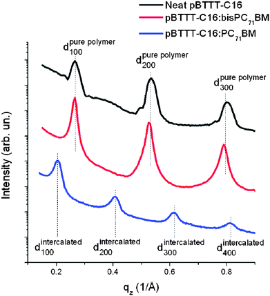 | ||
| Fig. 17 Grazing-incidence wide-angle X-ray diffraction patterns for pure pBTTT (black), pBTTT:bisPC71BM (red), and pBTTT:PC71BM (blue). Figure reproduced from ref. 112, Copyright © 2009, American Chemical Society. | ||
The results reviewed in Sections 3 and 4 clearly illustrate that the molecular structure of both the polymer and the fullerene components have a significant influence on the physical and optoelectronic properties of a binary photovoltaic blend. However the design and preparation of BHJ OPV devices containing three different materials in the photoactive layer has also attracted growing interest.116 In such ternary blend OPVs, a relatively small fraction of a semiconducting donor,117 acceptor,118 sensitizer,119 or block-polymer120 is added to a binary blend. Here, the third component (e.g. a semiconducting polymer) can extend the light-harvesting ability of the device if its optical absorption complements that of the primary polymer. The incorporation of the third component can also change the molecular order, or mixing and separation of the main components. Such morphology changes can be used to dramatically affect photo-physical processes and consequently modify device performance. However the presence of the third component in the BHJ layer increases the complexity of the ‘parameter-space’ associated with the choice of materials and processing conditions needed to optimize photovoltaic functionality. Until a rational design and optimization process has been reached, the benefit of such ternary blends cannot be fully realized.121 A description of the design rules and implications of BHJ OPVs based on ternary blends can be found in a number of dedicated reviews.122–124
5. Molecular conformation, phase separation and device performance upon thermal annealing
Thermal annealing is a post film-deposition technique that can modify the morphology of polymer:fullerene blend thin-films and thus impact upon their photovoltaic properties. For example, in PSBTBT:PCBM solar cells,125,126 thermal annealing can increase the crystallinity of PSBTBT and consequently improve charge carrier mobility. For many other copolymer systems however, thermal annealing has a negative impact upon OPV device efficiency. For example, in PCDTBT:PCBM devices, OPV PCE can be slightly improved only by thermal annealing below ∼80 °C however annealing above this temperature device efficiency is reduced. In devices based on many other low bandgap copolymers (for instance PBDTTPD127), thermal annealing even at relatively mild temperatures will reduce photovoltaic performance.As many D–A copolymers are relatively amorphous and exhibit fine mixing with fullerene molecules, it is a challenge to unambiguously characterize the nanoscale morphology in these blends. Synchrotron-based grazing incidence X-ray scattering measurements are able to reveal subtle changes in structure in these low-order systems that result from thermal annealing.128 In Fig. 18a, a 2D GIWAXS image of a PCDTBT thin film prepared by spin-casting from CB is presented.129 Here, it can be seen that π–π stacking in the as-cast PCDTBT film is evidenced by a scattering ‘crescent’ observed at q = 1.57 Å−1 in the out-of-plane direction. This indicates a preferential “face-on” π-stacked orientation of the polymer chains with respect to the silicon substrate. The inner diffraction ring, observed at qz = 0.31 Å−1 (∼20 Å) is attributed to 1st order scattering from the PCDTBT backbones separated by two alkyl side-chains. Recent work130 has shown that PCDTBT chains form lamellar structures with an “edge-on” orientation with respect to the plane of the film after thermal treatment. This is shown in Fig. 18b, in which a 2D GIWAXS scattering pattern from a PCDTBT thin film after thermal annealing at 200 °C is presented. Here, 2nd and 3rd order diffraction peaks from lamellar side-chain crystals at qz = 0.634 Å−1 and 0.947 Å−1 are observed in the out-of-plane direction. Several other off-axis peaks, located at (±0.150, 0.186), (±0.150, 0.494) and (±0.150, 0.811) Å−1, indicate extended long-range order along the backbone direction of the crystallites.130 We note that the development of “edge-on” lamellar crystals may well be determined by the temperature and kinetics of the thermal annealing treatment, and also by the molecular weight of the polymer. Nevertheless, the molecular structure in PCDTBT films upon thermal treatment above the bulk Tg is described by a combination of “face-on” π–π stacking and “edge-on” lamella ordering.128,130 Additional insight into nanostructure in PCDTBT thin-films can be obtained using GIWAXS performed as a function of X-ray beam grazing incidence angle, providing a degree of depth resolution below the film surface.129 It was shown that lamellar ordering in annealed PCDTBT thin films mainly occurs close to the film-surface, whilst π–π stacking is more pronounced toward the substrate interface.129 A key finding from this study was the demonstration that vertical heterogeneity in molecular structure can exist in PCDTBT thin-films, with the extent of such variations influenced by the surface and substrate interface.
 | ||
| Fig. 18 2D GIWAXS images of PCDTBT (a) in an as-cast state and (b) after thermal annealing. Figures reprinted from ref. 129 and 130, respectively. Copyright © 2012, Nature Publishing Group. | ||
Studies on PCDTBT128,131 have shown that the overall degree of π–π stacking in a thin-film reduces upon annealing, with such changes affecting the charge transport properties of the material (see Fig. 19). In an OPV device, charges are ideally transported between the electrodes in a direction perpendicular to the substrate. Consequently, “face-on” π–π stacking with respect to the device substrate is generally more favorable for efficient charge carrier transport than “edge-on” lamellar packing as the distance between π–π stacked molecules (∼4 Å) is significantly smaller than the distance between lamellae (∼20 Å). Changes in molecular structure of the polymer phase are therefore likely to be partly responsible for reduced out-of-plane charge mobility in PCDTBT:PC71BM blend thin-films upon thermal annealing around the bulk Tg.131 Further reductions in photovoltaic performance are found when higher annealing temperatures (at or above the Tg of PC71BM at ∼155 °C) are applied.131 In this regime, the thermally activated diffusion rate of PC71BM increases substantially and PC71BM molecules may aggregate to form micron-scale crystallites.131 The aggregation and crystallization of PC71BM reduces the fullerene concentration in the bulk of the blend film and consequently reduces the volume of interfaces with PCDTBT. It was suggested therefore that the morphological coarsening of the blend reduced device PCE by decreasing the efficiency of photogenerated charge separation and increasing charge-carrier recombination.
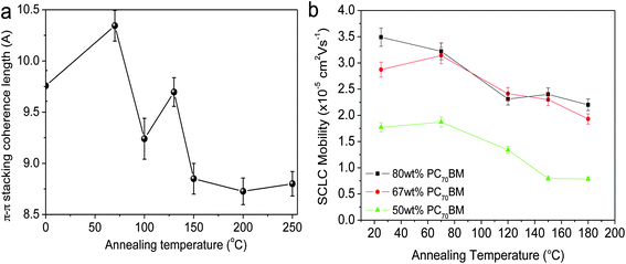 | ||
| Fig. 19 (a) The π–π stacking coherence length of PCDTBT in a thin film as a function of annealing temperature as measured by GIWAXS. (b) SCLC hole-carrier mobility of a PCDTBT:PC71BM thin-film device as a function of annealing temperature (annealing time of 30 minutes). Figure reprinted from ref. 131, Copyright © 2012 WILEY-VCH. | ||
Recent work127 on PBDTTPD:PC61BM blend thin-films has also found that lamellar ordering of the polymer increases and π–π stacking decreases after the film has been subject to thermal annealing; an effect similar to those observed in PCDTBT. Here however, it was found that the SCLC hole mobility in PBDTTPD was not significantly affected by annealing.127 The authors attributed the relatively lower PCE of thermally annealed devices to reduced miscibility between PCBM and PBDTTPD that led to the formation of morphological charge traps. Studies on OPV blends of poly(thienothiophene benzodithiophene) (PTB1) and PCBM have also demonstrated that thermal annealing reduces device efficiency.132 Here, GIWAXS measurements revealed that thermal annealing enhances π–π stacking between PTB1 chains, with these chains adopting a “face-on” orientation with respect to the film substrate. However, thermal annealing also resulted in the formation of relatively large PCBM domains having a size between 10 and 200 nm. This morphology – often described as ‘overly coarse phase-separation’ – is believed to reduce the efficiency of charge separation and was identified as the origin of the reduced device PCE.
In summary, although thermal annealing has been demonstrated to enhance the photovoltaic performance of solar-cell devices utilizing semi-crystalline copolymers (such as PSBTBT), it does not generally improve performance of devices based on amorphous copolymer blends.133,134
6. Molecular conformation, phase separation and device performance controlled via solvent processing
In this section, we review experiments designed to control the state of order and phase separation in D–A copolymer – fullerene blends through solvent processing. The solvent processing described here includes the use of different solvents, solvent mixtures, solvent additives and solvent vapor annealing.Polymer and fullerene components used in a BHJ often have a different solubility in different solvents. The use of different types of solvent or a mixture of solvents to dissolve a polymer:fullerene blend has been widely used to control the nanoscale morphology of the blend on casting from solution, with such blend morphology having a clear impact on device performance.135,136Fig. 20 shows the effect of casting solvent on film morphology and device performance for a PCDTBT:PC71BM blend solar cell.135 It can be seen that large clusters of PC71BM aggregates are present in films cast from CF and CB, whereas fine-scale phase separation occurs in the film cast from DCB. Such structure is present at the film surface (as measured by AFM) and in the bulk (as measured by TEM). It was found that OPV devices fabricated with the active layer cast from DCB had both the highest internal photocurrent efficiency (IPCE) and external device efficiency.
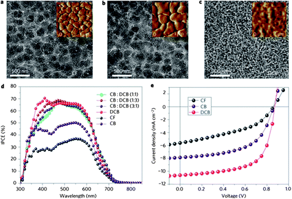 | ||
| Fig. 20 TEM images of PCDTBT:PC71BM films spin-cast from (a) CF, (b) CB and (c) DCB solvents. The insets show the surface phase images measured by atomic force microscopy (AFM). (d) IPCE spectra and (e) J–V characteristics of the devices fabricated with films cast from CF, CB and DCB. Figure reprinted from ref. 135, Copyright © 2009, Nature Publishing Group. | ||
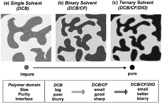
The use of solvent mixtures to cast a photovoltaic blend film has been found to exert a dramatic influence on the molecular packing of each material and the overall BHJ morphology. This is shown in the schematic illustration presented in Fig. 21 which describes a blend of the materials PDPP3T:PC71BM.137 When the blend is cast from DCB, the film is characterized by large, impure (mixed) domains separated by rough interfaces. The addition of 20% CF to DCB however leads to a remarkable increase in domain purity that is accompanied by reduced domain size and sharper interfaces. On addition of 5% of the solvent additive 1,8-diiodooctane (DIO) to the DCB/CF solvent, the interface between domains becomes rougher, however the size of the domains is not apparently affected. Furthermore grazing incidence X-ray scattering shows that pronounced diffraction peaks of the PDPP3T component are observed due to improved lamellar order.137 Ternary mixed solvents treatment can thus be used to improve molecular morphology for OPV applications through the formation of long-range ordered structures having favorable, pure domains characterized by rough domain interfaces. As a result, the PCE of PDPP3T:PC71BM solar cells was improved from 4.87 to 5.38 and then to 6.71%, when the blends were cast from DCB, DCB/CF and DCB/CF/DIO, respectively.137
 | ||
| Fig. 21 Schemes of morphology evolution in PDPP3T/PC71BM blend films cast using different solvents. Figure reprinted from ref. 137, Copyright © 2012 WILEY-VCH. | ||
The differing solubility of the polymer and fullerene components in solvent mixture can also lead to the formation of a film morphology characterized by multiple length-scales. For example the polymer pDPP dissolves well in the low boiling point solvent CF, but is less soluble in higher boiling point solvent DCB. In contrast however, PC71BM is more soluble in DCB compared to CF. Therefore if a pDPP:PC71BM blend film is cast from a DCB/CF solvent mixture,138 the initial rapid evaporation of the lower boiling point CF causes the pDPP to become relatively less soluble, causing it to crystallize. The PC71BM however remains solvated as the casting solvent contains a significant fraction of DCB. As a result of this, the dried film is characterized by a crystalline fibrillar network composed of pDPP that is surrounded by fine-scale phase-separated pDPP/PC71BM morphology formed during the latter stages of the film drying process.
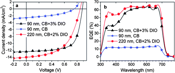
The addition of a few vol% of a solvent additive to the primary casting solvent has been demonstrated to be an effective means to improve the PCE of BHJ OPVs made from D–A copolymers.139 For example, OPVs made from PCPDTBT:PC71BM had a PCE of 2.7 to 3.5% without the inclusion of any type of solvent additive.140,141 However by incorporating a small amount of alkanedithiol as an additive to the primary solvent (chlorobenzene), the PCE was increased to 5.5%. In other work, PDTSTPD:PC71BM OPV devices processed using the additive DIO (at 3% by volume) have yielded device PCEs close to 7.3%; a dramatic increase over PCEs of less than 1% when no additive is used (see Fig. 22).142 It is worthwhile to note that with the addition of DIO, a PCE of 6.1% can be obtained in OPV devices having an area of 1.0 cm2 even when the active layer is 220 nm thick.
 | ||
| Fig. 22 (a) J–V and (b) EQE curves of solar cells made from PDTSTPD:PC71BM (1:2) blend with/without the presence of solvent additive DIO at different thickness of the active layer. Figure reprinted from ref. 142, Copyright © 2011 American Chemical Society. | ||
In order for a solvent additive to modify the morphology of BHJ polymer:fullerene blend thin-films during the film-casting process, it must exhibit a higher boiling point than the primary solvent and also a preferential solubility for PCBM.143,144 This effect has been studied in detail using D–A copolymers such as PTB7,145 PBTTPD,24 PCPDTBT,144,146,147 PDPPTPT,148 PSi and PGe.149 Here, the use of techniques that probe the structure of such blend thin-films has demonstrated that solvent additives can significantly alter the nanoscale morphology of the bulk heterojunction system. Indeed, solvent additives are able to reduce the size of fullerene domains or improve their average state of structural order. For example, TEM studies of PBTTPD:PC71BM blend thin-films has revealed a reduction in fullerene domain size from 150 nm to ∼30 nm upon addition of the additive diiodohexane (DIH) to the casting solution.24 This effect can also be seen in the TEM images presented in Fig. 23, where a relatively finely mixed morphology was observed in a PTB7:PC71BM blend thin-film upon on addition of 3 vol% diiodooctane (DIO) to the casting solution.145 Resonant soft X-ray scattering (R-SoXS) measurements suggested that a fullerene domain size of 177 nm in PTB7:PC71BM blend films cast from CB was reduced to ∼34 nm when DIO was added to the casting solvent.150 In a related study, transmission SAXS measurements on solution samples revealed that DIO can selectively dissolve PCBM aggregates in a PTB7:PC71BM blend solution, permitting the formation of a more finely mixed blend morphology when the solution is cast into a thin-film.151 GIWAXS has been used to study the modification of blend structure at a molecular length-scales resulting from the incorporation of a solvent additive. Here it was found that the PTB7 lamellar d-spacing underwent a small increased from 17.1 to 18.9 Å relative to a blend film that was cast without the DIO additive. However, no substantial changes in the length-scale of either PTB7 π–π stacking or the packing of PCBM molecules was identified.
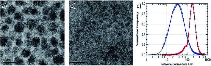 | ||
| Fig. 23 TEM images of PTB7/PC71BM (1:1.5) films cast (a) without and (b) with the additive DIO. Scale bar 200 nm. (c) Normalized histogram of scattering intensity versus fullerene domain size in PTB7/PC71BM with (blue curve) and without (red curve) DIO as measured by R-SoXS. Figures reprinted from ref. 145 and 150, Copyright © WILEY-VCH. | ||
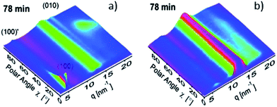
Solution processing additives can result in an increased degree of polymer crystallinity. This has been demonstrated using GISAXS/GIWAXS in PBTTPD:PC71BM blends upon the addition of DIH to the primary casting-solvent chloroform (CF).24 This conclusion was also confirmed in a second study where the polymer PCPDTBT was found to crystallize through the presence of solvent additives.143,152–154 Using time-resolved GIWAXS, Rogers et al.153 observed a lower nucleation barrier for PCPDTBT crystallization upon addition of octanedithiol (ODT) to the primary casting solvent, thereby encouraging crystallite growth over an extended timescale. This effect is illustrated in Fig. 24, where GIWAXS scattering patterns from a PCDPTBT:PC71BM 1:3 wt% blend film cast from CB or CB/ODT after 78 minutes after spin casting is shown. Here, it can be seen that films cast from CB/ODT solutions show pronounced Bragg scatter originating from the (100) plane of semi-crystalline PCPDTBT. As demonstrated in an earlier study, the crystallization of PCPDTBT is unimpeded by the presence of PCBM, which – as a result of the solvent additive – remains relatively well-dissolved in solution.152 This suggested that the additive facilitates the formation of a multi-length scale morphology comprising domains of pure, crystalline PCPDTBT fibrils and a PCBM-rich mixture containing amorphous PCPDTBT.152 It was argued that the formation of such structures was not possible via conventional thermal annealing techniques as polymer self-organization is inhibited by the simultaneous thermally activated diffusion of PCBM molecules. Accordingly, the morphology formed by solvent mixtures can (to a certain extent) be described as being ‘non-equilibrium’ in nature.152
 | ||
| Fig. 24 3D sector plots of PCPDTBT:PC71BM blends cast from CB containing (a) 3% or (b) 0% ODT after 78 min of spin-coating, showing the scattered intensity vs. polar angle χ and scattering vector q. Figure reprinted from ref. 153, Copyright © 2012, American Chemical Society. | ||
Although it has often been observed that the use of solvent additives can improve the PCE of an OPV device. This is, however, not true in some cases. For example, the addition of DIO to a PCBM blend containing a N-alkylthieno[3,4-c]pyrrole-4,6-dione (TPD)-based polymer having linear side-chains only had a marginal effect on OPV properties.155 This finding was explained on the basis that the copolymer already forms relatively ordered structures when cast from the primary solvent. In other work it was shown that the addition of 3 vol% DIO to the primary casting-solvent (CB) results in a relatively large increase in the PCE of a PDTSTPD/PC71BM blend OPV (from below 1.0% to 7.3%), however such effects are less pronounced when the primary solvent is switched to DCB.142 A similar conclusion has also been reached when DIO was used as an additive in a DCB-cast PTB7/PC71BM blend device.145 It is clear therefore that there is a complex interdependence between the nature and properties of the additive, the polymer and the primary casting solvent.
Subjecting photovoltaic blends to a solvent vapor is a technique that can also be used to tune the nanoscale morphology and thus modify OPV device performance.61,156 For example, it was found that an interpenetrating network having nanoscale phase separation can be created in PCDTBT:PC71BM blend by annealing it in a mixed solvent vapor comprising a 1:1 blend of THF:CS2 for 5 minutes.157 Here, the CS2 vapor is a good solvent for PCDTBT and thus helps to improve both crystallinity and degree of π–π stacking within the PCDTBT phase; a conclusion reached on the basis of X-ray measurements. TEM studies of the same blend also demonstrated the ability of the PCDTBT phase to self-organize to form nanofibrils. However the THF component of the vapor induced the PC71BM to form aggregates and to phase separate from the mixed phase, with the CS2 vapor preventing the formation of excessively large aggregates. As a result, the efficiency of vapour annealed devices increased from 4.5 to 6.6%; an increase in efficiency by more than 40% over that of the untreated device.
7. Vertical stratification of PCBM in copolymer solar cells
Vertical stratification of electron donors and acceptors within a BHJ layer can be induced during the film casting process or during the application of post film-deposition annealing treatments. The degree of stratification is often determined by the molecular interactions between the polymer chains and the fullerene molecules, and by the interactions between these materials and the film substrate. In an OPV device, vertical stratification is often believed to have an important influence on the efficiency of charge transport within the BHJ layer and the eventual extraction of charge at the electrode interfaces. For example, a relatively high concentration of the hole-transporting polymer at the cathode interface will impede electron extraction, whereas an enriched layer of electron-transporting fullerenes at the anode interface will reduce the efficiency of hole extraction by acting as a charge recombination centre. A number of techniques have been used to characterize chemical composition at or close to the surface of a film, including near-edge X-ray absorption fine-structure (NEXAFS)158 and X-ray photoelectron spectroscopy (XPS).159 Other techniques have been used to probe the entire depth profile of the components in a blend including neutron reflectivity (NR),160 X-ray reflectivity (XRR),161 spectroscopic ellipsometry (SE)162 and dynamic secondary ion mass spectrometry (DSIMS).126Using XPS Felicissimo et al.159 detected an enriched polymer layer at the film surface in an F8DTBT:PC61BM blend. DSIMS and NEXAFS were used by Anselmo et al.158 to study the vertical profile of donor–acceptor polyfluorene copolymers blended with PC61BM, and also evidenced an enrichment layer of polymer near the film surface. Here, the purity of the enrichment layer improved as the polar nature of the polymer was increased. Lu et al.126 reported a PSBTBT enriched-layer at the film surface in an as-cast PSBTBT:PC61BM blend films. In this system, it was found that thermal annealing promoted the segregation of PSBTBT to the film surface in the absence of a cathode layer (see Fig. 25a), however this process was apparently reversed, with migration of PC61BM toward the top surface observed when the blend film was annealed in the presence of a cathode (see Fig. 25b).
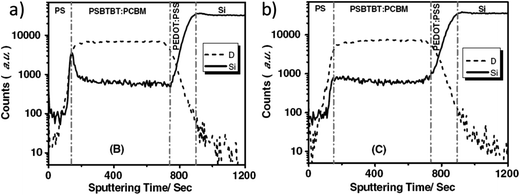 | ||
| Fig. 25 DSIMS profile of PSBTBT:PC61BM blend films annealed at 150 °C for 1 min (a) before and (b) after the deposition of the Al cathode. Figure reprinted from ref. 126, Copyright © 2011 WILEY-VCH. | ||
The vertical stratification of PCBM in PCDTBT:PC61BM blend films has been studied using NR.160 Here, it was shown that there was an enrichment of PCBM at the film surface in an as-cast PCDTBT:d5-PC61BM 1:4 wt% blend spin-cast on a PEDOT:PSS anode film. At the interface with the anode, there was also a relative depletion of the fullerene, effectively constituting an enriched PCDTBT layer.160 Such a distribution of donor and acceptor materials is ideal in OPV devices fabricated in a standard geometry (cathode on top), since efficient charge extraction is facilitated by the enrichment of the electron accepting material when it is located close to the cathode. A follow-on NR study probed the generality of this vertical structure by measuring the depth composition of PCDTBT-8:PC71BM (defined as P1:PC71BM in ref. 163) and PCDT2BT-8:PC71BM (defined as P2:PC71BM in ref. 163) 1:4 wt% blend thin films spray-cast onto a heated PEDOT:PSS substrate.163 It was found that the vertical stratification observed was qualitatively similar to that seen in PCDTBT:PC71BM. This can be seen in Fig. 26, where for films spray-cast onto a substrate held at 40 °C, it is apparent that there is a region close to the PEDOT:PSS interface in which the PC71BM concentration is relatively deficient. The degree of vertical stratification observed is apparently dependent on the temperature of the underlying substrate during film drying. For a substrate temperature of 40 °C, the average width and relative weight concentration of the PC71BM depleted region was 17 nm and 65 wt% respectively. At a substrate temperature of 60 °C, the PC71BM concentration in the deficient region increased to 78 wt% whilst the width of this region decreased to 13 nm. For blend films cast onto a substrate held at 80 °C the deficient region was almost completely suppressed, indicating a relatively homogeneous distribution of PC71BM throughout the entire depth of the blend film. This clearly demonstrates the possibility to alter vertical stratification in these blend films by accelerating the film casting process though the use of a heated substrate.
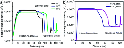 | ||
| Fig. 26 (a) Scattering length density (SLD) profiles of PCDTBT:PC71BM (1:4) blends deposited by spray-coating at three different substrate temperatures from a CB solution. (b) SLD profiles of P1:PC71BM and P2:PC71BM blends deposited by spray-coating at a substrate temperature of 40 °C from a CB solution. The thicknesses of the blend films are slightly different for all samples. Figures reprinted from ref. 163, Copyright © 2013 WILEY-VCH. | ||
Although there are large number of D–A copolymers that have been demonstrated to be very promising electron donating materials, there has only been a limited amount of work reported that addresses the extent of vertical stratification in a BHJ active layer and its consequence for efficient OPV operation. At present, more work is needed to fully explore the effects of free energy of each component, the role of polymer–fullerene and blend–substrate interactions as well as the film drying kinetics on driving vertical distribution of the different blend components. We believe that such studies will help to establish a clear correlation between the vertical component distribution and device performance.
8. Morphological stability
The stability of the active layer morphology and the electrode interfaces have a dramatic influence on the operational lifetime of a solar cell device. As the active layer of a polymer–fullerene BHJ solar cell is prepared from solution, a few percent of casting solvent can become trapped within the film during the film drying process.131 Such residual solvents can induce the diffusion and aggregation of the PCBM component, and ultimately affect the stability of the film morphology.164 Residual solvents often can only escape from a solid blend film very slowly as their evaporation is opposed by the slow volume-relaxation of the glassy film.165 Ye et al. demonstrated that by washing a photovoltaic blend with a low boiling-point inert solvent (such as methanol), it was possible to remove unwanted solvent additives.166 Here, the removal of high boiling point solvent additives has been found to enhance device performance and morphological stability. This method has proved to be effective in a number photovoltaic blends of PC71BM incorporating different donor polymers.Another technique used to remove trapped, residual solvent is to heat a blend film at a temperature above the Tg of the blend or the boiling temperature of the specific solvent.16,131 However heating at high temperatures increase the diffusion coefficient of PCBM and encourages aggregation.131 Once the size of the PCBM aggregates and the extent of phase separation becomes too coarse, detrimental effects can occur to limit device efficiency.127,131 Recent work has demonstrated that low-level light exposure (with an illumination intensity ∼10 mW cm−2) before low-temperature thermal annealing can be used to significantly increase the thermal stability of PCDTBT:PC61BM solar cell devices.167 Here, the enhanced stability upon light exposure was suggested to result from the dimerization or oligomerization of PC61BM; an effect assumed to slow down the diffusion and crystallization of PCBM under thermal stress.168 It was suggested that the effect was more effective in a PC61BM based-blend compared to that containing PC71BM, as C60 has greater tendency to undergo photo-induced crosslinking.167 However a different study on a blend of PDTSTzTz:PC61BM found that the charge carrier mobility in an OPV device underwent a significant reduction upon light exposure (with an illumination intensity ∼100 mW cm−2) caused by the optically-induced dimerization of PC61BM.169 The same study also reported that photo-induced dimerization did not occur in the fullerene derivative bisPC61BM.
Poly(3,4-ethylenedioxythiophene):polystyrene sulfonate (PEDOT:PSS) is widely used as the hole transporting layer in organic solar cells. However its acidic and hygroscopic nature make it susceptible to degradation, but also can result in the degradation of the active semiconductor layer and the device electrodes.170 Furthermore, the adsorption and transport of moisture by the PEDOT:PSS anode-buffer into the active layer can also enhance ionic conduction of the active layer and accelerate corrosion.171 A cross-sectional TEM study reported by Suh et al. showed that the Ag electrode layer was degraded into particles of ∼10 s of nm over time in an inverted solar cell comprising of Ag/PEDOT:PSS/P3HT:PCBM/TiO2/ITO/glass.170 It was speculated that the water absorbed by the PEDOT:PSS layer caused corrosion at grain boundaries within the Ag layer. Indeed, it has been shown that by replacing PEDOT:PSS with a more air-stable hole-transporting layer (such as MoOx), the operational life-time of an OPV can be increased.172
While the use of alternative electrode materials having greater stability is an effective way to improve interface stability, the stability of the active layer requires the use of stable electron-donor and -acceptor materials.173 The synthesis of new polymers for high efficiency thus needs to also combine high stability on exposure to oxygen, water, and light as well as to thermal stress, as described in a guide to the role of the polymer structure on determining photochemical stability.174 Other approaches to increasing the morphological stability of the active layer by cross-linking the polymer175,176 or the fullerene177 have also been proposed.
9. Incorporation of interlayers in copolymer solar cells
The incorporation of an interlayer between the polymer:fullerene active layer and the electrodes has been demonstrated to be an efficient approach to improve the PCE of various D–A copolymer solar cells.178 Conjugated polyelectrolytes, uncharged conjugated polymers, saturated polymers and small organic molecules have all been employed as an interlayer material. The mechanism behind such improvements has often been assigned to changes of electronic and orbital interactions at the interface. In this section, we discuss the use of such interface materials with D–A copolymer blends (see chemical structures in Fig. 27) and highlight cases where significant improvements in OPV device efficiency have been gained.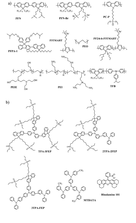 | ||
| Fig. 27 The chemical structure of a range of (a) polymers and (b) small molecules that have been employed as interlayer in OPVs. | ||
He et al.179 reported simultaneous enhancement of Voc, Jsc and FF in OPVs made by incorporating the alcohol/water-soluble conjugated polyelectrolyte PFN between the cathode and the active layer. As a result, OPV PCEs of 6.79% and 8.37% were achieved using PCDTBT and PTB7 polymer:fullerene blends. Scanning Kelvin probe microscopy measurements indicate that in this system a microscopic electric dipole exists at the interface. This particular dipole alignment enhances the built-in potential and was estimated to be 0.3 V for 5 nm thick PFN layer. This enhanced built-in potential can improve charge-extraction, reduce the buildup of space-charge, and thus reduce recombination. The effective work-function of the ITO anode after coating a PFN interlayer has been found to reduced from 4.7 to 4.1 eV from X-ray photoelectron spectroscopy measurement.3 A PCE of 9.2% could be obtained by incorporating a PFN interlayer in the inverted OPV based on PTB7:PC71BM blend.3 Recently, Xia et al.180 found a non-monotonic variation of device performance that was dependent on the thickness of the PFN interlayer in an inverted OPV containing a PCDTBT:PC71BM blend. It was found that a higher PCE could be achieved when the thickness of the PFN layer was between 8 and 12 nm. The use of a PFN interlayer has also been found to be an effective approach to improve the efficiency of OPVs made using the low bandgap polymers PCz-DTBTA181 and PECz-DTQx.182
A number of other interlayer materials (see Fig. 27 for the molecular structure of these materials) have been used with D–A polymer:fullerene blends to good effect. Yang et al.183 demonstrated an increase in PCE from 6.1% to 8.4% by inserting a PFN-Br polyelectrolyte layer between a ZnO cathode and a PBDT-DTNT:PC71BM active layer in an inverted device. The inclusion of the interfacial PFN-Br layer was believed to provide good interfacial contact and adhesion, to facilitate electron transport and to suppress bimolecular recombination, leading to an increased Voc, Jsc and FF.184 PFNBR and PSFNBr have been found to improve the performance of OPVs based on PFOTBT:PC61BM.185 Cationic conjugated polymer electrolytes such as P3TMAHT, PF2/6-b-P3TMAHT have also been shown to improve the efficiency of PCDTBT:PC71BM OPVs when they are incorporated as a OPV interlayer.186 The use of a uncharged conjugated polymer (PFPA-1) was reported as an interlayer between a TQ1:PC71BM active layer and a TiOx/Al cathode. Here the PFPA-1 layer was believed to act as a hole-blocking layer and also to modify the substrate surface energy and generate a finer morphology in the active layer.187 A homopolymer of 2,7-carbazole with hydrophilic phosphonate side chains (PC-P) was used as an interlayer on ITO, and was reported to improve the PCE of OPVs made from PCDTBT12 from 5.53% to 6.04%.188 It was proposed that the hydrophilic side chains of PC-P introduced a sub-gap state that facilitated electron transport. TFB has been incorporated between the hole-transporting layer and the active layer in OPV devices to improve device performance via its electron-blocking ability.189,190
The saturated polymer poly(ethylene oxide) (PEO) deposited on the electrode ZnO was found to improve device performance of OPVs made from TQ1 and PCDTBT. PEO was believed to modify the ZnO by passivating surface traps, suppressing charge recombination, reducing device series resistance and improving the electrical coupling between ZnO and the active layer.191 Zhou et al.192 reported that an ultrathin polymer layer containing simple aliphatic amine groups (such as PEIE or PEI) that is physisorbed onto a conductor surface (e.g. a metal, metal oxide, conducting polymer, graphene etc.) can act as a “universal” surface modifier to create low-work function electrodes for organic electronics. Chen et al.193 have developed a new family of neutral alcohol-soluble small organic molecules as the cathode interlayer (namely 3TPA-FEP, 2TPA-2FEP and TPA-3FEP) that comprise of electron-rich triphenylamine (TPA) and fluorine that are decorated with phosphonate side chains (FEP). A high PCE of 7.21%, 6.90% and 6.89% was achieved in PCDTBT:PC71BM devices using 3TPA-FEP, 2TPA-2FEP and TPA-3FEP respectively positioned between Al and the active layer. Such PCEs are among the highest reported for OPVs based on this particular blend. Other work has demonstrated that small organic molecules such as MTDATA194 and Rhodamine 101 (ref. 195) can also be successfully applied as interlayers in OPVs containing D–A copolymers.
10. Summary and outlook
The donor–acceptor concept provides a facile approach to tune the physical and optoelectronic properties of donor–acceptor copolymers as the electron-donating component in organic photovoltaic devices. Many novel donor–acceptor copolymers have been synthesized in the past few years, and have promoted a rapid development of high performance bulk heterojunction organic solar cells. Power conversion efficiencies above 10% have now been demonstrated in organic bulk heterojunction solar cells using these D–A materials. As we have described here, several strategies exist to synthesize D–A copolymers having relatively low optical band-gaps, favorable energy levels and ICT characteristics though the rational choice of donor and acceptor moieties, substitution units, branching units and the size and position of solubilizing side-groups. We have also shown that the application of novel donor–acceptor copolymers in the creation of high performance solar cells requires the formation of a nanoscale morphology and optoelectronic properties that favor absorption of sunlight, exciton splitting and charge-carrier collection processes. Various morphological probes (e.g. high resolution TEM and energy filtered TEM) and scattering techniques (e.g. X-ray scattering, neutron scattering) have been employed to explore the nanoscale morphology in bulk heterojunction blends (e.g. molecular packing and ordering, nanoscale aggregation, 3D connectivity, etc.). Such morphological investigations – in both lateral and vertical directions – have been used to correlate various processing conditions with device performance, and ultimately provide feedback to synthetic chemists in the design of new polymer donors.Whilst the past few years has evidenced a rapid increase in the efficiency of organic solar cells, there are still many challenges to be met in translating laboratory-scale demonstrations into practical applications. These challenges include increasing device stability and lifetime, the scale up from small-scale to large-scale using solution-based deposition processes such as roll-to-roll production, spray coating and inkjet printing. Such challenges will clearly require close, interdisciplinary collaboration between chemists, physicists and engineers having a direct interest in thin-film manufacturing techniques.
Acknowledgements
We thank financial support from EPSRC via grant EP/I028641/1 “Polymer/fullerene photovoltaic devices: new materials and innovative processes for high-volume manufacture” and EP/J017361/1 “Supersolar Solar Energy Hub”. AJP thanks King Abdulaziz University for financial support via grant no. D-004/431. We thank Lucy Pickford (Ossila Limited, UK) for preparing the TOC image of this paper.References
- G. Dennler, M. C. Scharber and C. J. Brabec, Adv. Mater., 2009, 21, 1323 CrossRef CAS.
- P. W. M. Blom, V. D. Mihailetchi, L. J. A. Koster and D. E. Markov, Adv. Mater., 2007, 19, 1551 CrossRef CAS.
- Z. He, C. Zhong, S. Su, M. Xu, H. Wu and Y. Cao, Nat. Photonics, 2012, 6, 591 Search PubMed.
- J. You, L. Dou, K. Yoshimura, T. Kato, K. Ohya, T. Moriarty, K. Emery, C.-C. Chen, J. Gao, G. Li and Y. Yang, Nat. Commun., 2013, 4, 1446 CrossRef PubMed.
- L. Bian, E. Zhu, J. Tang, W. Tang and F. Zhang, Prog. Polym. Sci., 2012, 37, 1292 CrossRef CAS PubMed.
- C. H. Duan, F. Huang and Y. Cao, J. Mater. Chem., 2012, 22, 10416 RSC.
- H. X. Zhou, L. Q. Yang and W. You, Macromolecules, 2012, 45, 607 CrossRef CAS.
- M. Mayukh, I. H. Jung, F. He and L. Yu, J. Polym. Sci., Part B: Polym. Phys., 2012, 50, 1057 CrossRef CAS.
- P.-L. T. Boudreault, A. Najari and M. Leclerc, Chem. Mater., 2011, 23, 456 CrossRef CAS.
- J. Rivnay, S. C. B. Mannsfeld, C. E. Miller, A. Salleo and M. F. Toney, Chem. Rev., 2012, 112, 5488 CrossRef CAS PubMed.
- D. M. Delongchamp, R. J. Kline and A. Herzing, Energy Environ. Sci., 2012, 5, 5980 CAS.
- W. Chen, M. P. Nikiforov and S. B. Darling, Energy Environ. Sci., 2012, 5, 8045 CAS.
- T. Wang, A. D. F. Dunbar, P. A. Staniec, A. J. Pearson, P. E. Hopkison, J. E. Macdonald, S. Lilliu, C. Pizzey, N. J. Terrill, A. M. Donald, A. J. Ryan, R. A. L. Jones and D. G. Lidzey, Soft Matter, 2010, 6, 4128 RSC.
- B. Schmidt-Hansberg, M. Sanyal, M. F. G. Klein, M. Pfaff, N. Schnabel, S. Jaiser, A. Vorobiev, E. Müller, A. Colsmann, P. Scharfer, D. Gerthsen, U. Lemmer, E. Barrena and W. Schabel, ACS Nano, 2011, 5, 8579 CrossRef PubMed.
- A. J. Pearson, T. Wang and D. G. Lidzey, Rep. Prog. Phys., 2013, 76, 022501 CrossRef PubMed.
- T. Wang, A. J. Pearson, R. A. L. Jones and D. G. Lidzey, Adv. Funct. Mater., 2011, 21, 1383 CrossRef CAS.
- T. Agostinelli, S. Lilliu, J. G. Labram, M. Campoy-Quiles, M. Hampton, E. Pires, J. Rawle, O. Bikondoa, D. D. C. Bradley, T. D. Anthopoulos, J. Nelson and J. E. Macdonald, Adv. Funct. Mater., 2011, 21, 1701 CrossRef CAS.
- S. Lilliu, T. Agostinelli, E. Pires, M. Hampton, J. Nelson and J. E. Macdonald, Macromolecules, 2011, 44, 2725 CrossRef CAS.
- E. Verploegan, C. E. Miller, K. Schmidt, Z. Bao and M. F. Toney, Chem. Mater., 2012, 24, 3923 CrossRef.
- I. Osaka, M. Shimawaki, H. Mori, I. Doi, E. Miyazaki, T. Koganezawa and K. Takimiya, J. Am. Chem. Soc., 2012, 134, 3498 CrossRef CAS PubMed.
- J.-M. Jiang, P.-A. Yang, T.-H. Hsieh and K.-H. Wei, Macromolecules, 2011, 44, 9155 CrossRef CAS.
- G.-Y. Chen, Y.-H. Cheng, Y.-J. Chou, M.-S. Su, C.-M. Chen and K.-H. Wei, Chem. Commun., 2011, 47, 5064 RSC.
- J.-M. Jiang, M.-C. Yuan, K. Dinakaran, A. Hariharan and K.-H. Wei, J. Mater. Chem. A, 2013, 1, 4415 CAS.
- M.-S. Su, C.-Y. Kuo, M.-C. Yuan, U.-S. Jeng, C.-J. Su and K. H. Wei, Adv. Mater., 2011, 23, 3315 CrossRef CAS PubMed.
- H.-H. Cho, T. E. Kang, K.-H. Kim, H. Kang, H. J. Kim and B. J. Kim, Macromolecules, 2012, 45, 6415 CrossRef CAS.
- J. Guo, Y. Liang, J. Szarko, B. Lee, H. J. Son, B. S. Rolczynski, L. Yu and L. X. Chen, J. Phys. Chem. B, 2010, 114, 742 CrossRef CAS PubMed.
- J. M. Szarko, J. Guo, B. S. Rolczynski and L. X. Chen, J. Mater. Chem., 2011, 21, 7849 RSC.
- Y. Liang, Y. Wu, D. Feng, S.-T. Tsai, H.-J. Son, G. Li and L. Yu, J. Am. Chem. Soc., 2009, 131, 56 CrossRef CAS PubMed.
- J. Peet, A. J. Heeger and G. C. Bazan, Acc. Chem. Res., 2009, 42, 1700 CrossRef CAS PubMed.
- B. C. Thompson and J. M. J. Frechet, Angew. Chem., Int. Ed., 2008, 47, 58 CrossRef CAS PubMed.
- N. D. Treat, M. A. Brady, G. Smith, M. F. Toney, E. J. Kramer, C. J. Hawker and M. L. Chabinyc, Adv. Energy Mater., 2011, 1, 82 CrossRef CAS.
- A. C. Mayer, M. F. Toney, S. R. Scully, J. Rivnay, C. J. Brabec, M. Scharber, M. Koppe, M. Heeey, I. McCulloch and M. D. McGehee, Adv. Funct. Mater., 2009, 19, 1173 CrossRef CAS.
- R. Noriega, J. Rivnay, K. Vandewal, F. P. V. Koch, N. Stingelin, P. Smith, M. F. Toney and A. Salleo, Nat. Mater., 2013 DOI:10.1038/nmat3722.
- B. A. Collins, Z. Li, J. R. Tumbleston, E. Gann, C. R. McNeill and H. Ade, Adv. Energy Mater., 2012, 3, 65 CrossRef.
- P. Sista, B. Xue, M. Wilson, N. Holmes, R. S. Kularatne, H. Nguyen, P. C. Dastoor, W. Belcher, K. Poole, B. G. Janesko, M. C. Biewer and M. C. Stefan, Macromolecules, 2012, 45, 772 CrossRef CAS.
- F. C. Jamieson, E. B. Domingo, T. McCarthy-Ward, M. Heeney, N. Stingelin and J. R. Durrant, Chem. Sci., 2012, 3, 485 RSC.
- P. Westacott, J. R. Tumbleston, S. Shoaee, S. Fearn, J. H. Bannock, J. B. Gilchrist, S. Heutz, J. deMello, M. Heeney, H. Ade, J. Durrant, D. S. McPhail and N. Stingelin, Energy Environ. Sci., 2013, 6, 2756 CAS.
- M. C. Scharber, D. Mühlbacher, M. Koppe, P. Denk, C. Waldauf, A. J. Heeger and C. L. Brabec, Adv. Mater., 2006, 18, 789 CrossRef CAS.
- J.-L. Brédas, D. Beljonne, V. Coropceanu and J. Cornil, Chem. Rev., 2004, 104, 4971 CrossRef PubMed.
- Y. Li, Acc. Chem. Res., 2012, 45, 723 CrossRef CAS PubMed.
- Z.-G. Zhang, J. Min, S. Zhang, J. Zhang, M. Zhang and Y. Li, Chem. Commun., 2011, 47, 9474 RSC.
- R. Mondal, S. Ko, E. Verploegen, H. A. Becerril, M. F. Toney and Z. Bao, J. Mater. Chem., 2011, 21, 1537 RSC.
- D. H. Kim, A. L. Ayzner, A. L. Appleton, K. Schmidt, J. Mei, M. F. Toney and Z. Bao, Chem. Mater., 2013, 25, 431 CrossRef CAS.
- T.-Y. Chu, J. Lu, S. Beaupre, Y. Zhang, J.-R. Pouliot, J. Zhou, A. Najari, M. Leclerc and Y. Tao, Adv. Funct. Mater., 2012, 22, 2345 CrossRef CAS.
- Z. Li, S.-W. Tsang, X. Du, L. Scoles, G. Robertson, Y. Zhang, F. Toll, Y. Tao, J. Lu and J. Ding, Adv. Funct. Mater., 2011, 21, 3331 CrossRef CAS.
- A. T. Yiu, P. M. Beaujuge, O. P. Lee, C. H. Woo, M. F. Toney and J. M. J. Frechet, J. Am. Chem. Soc., 2012, 134, 2180 CrossRef CAS PubMed.
- C. Cabanetos, A. E. Labban, J. A. Bartelt, J. D. Douglas, W. R. Mateker, J. M. J. Fréchet, M. D. McGehee and P. M. Beaujuge, J. Am. Chem. Soc., 2013, 135, 4656 CrossRef CAS PubMed.
- J. M. Szarko, J. Guo, Y. Liang, B. Lee, B. S. Rolczynski, J. Strzalka, T. Xu, S. Loser, T. J. Marks, L. Yu and L. X. Chen, Adv. Mater., 2010, 22, 5468 CrossRef CAS PubMed.
- Y. Li, Y. Chen, X. Liu, Z. Wang, X. Yang, Y. Tu and X. Zhu, Macromolecules, 2011, 44, 6370 CrossRef CAS.
- L. Huo, J. Hou, S. Zhang, H.-Y. Chen and Y. Yang, Angew. Chem., Int. Ed., 2010, 49, 1500 CrossRef CAS PubMed.
- L. Huo, X. Guo, S. Zhang, Y. Li and J. Hou, Macromolecules, 2011, 44, 4035 CrossRef CAS.
- M. Wang, X. Hu, P. Liu, W. Li, X. Gong, F. Huang and Y. Cao, J. Am. Chem. Soc., 2011, 133, 9638 CrossRef CAS PubMed.
- L. Huo, S. Zhang, X. Guo, F. Xu, Y. Li and J. Hou, Angew. Chem., Int. Ed., 2011, 50, 9697 CrossRef CAS PubMed.
- Y. Huang, X. Guo, F. Liu, L. Huo, Y. Chen, T. P. Russell, C. C. Han, Y. Li and J. Hou, Adv. Mater., 2012, 24, 3383 CrossRef CAS PubMed.
- P. M. Oberhumer, Y.-S. Huang, S. Massip, D. T. James, G. Tu, S. Albert-Seifried, D. Beljonne, J. Cornil, J.-S. Kim, W. T. S. Huck, N. C. Greenham, J. M. Hodgkiss and R. H. Friend, J. Chem. Phys., 2011, 134, 114901 CrossRef PubMed.
- Q. Shi, H. Fan, Y. Liu, J. Chen, L. Ma, W. Hu, Z. Shuai, Y. Li and X. Zhan, Macromolecules, 2011, 44, 4230 CrossRef CAS.
- E. Wang, M. Wang, L. Wang, C. Duan, J. Zhang, W. Cai, C. He, H. Wu and Y. Cao, Macromolecules, 2009, 42, 4410 CrossRef CAS.
- S. K. Lee, S. Cho, M. Tong, J. H. Seo and A. J. Heeger, J. Polym. Sci., Part A: Polym. Chem., 2011, 49, 1821 CrossRef CAS.
- H. Zhou, L. Yang, S. Xiao, S. Liu and W. You, Macromolecules, 2010, 43, 811 CrossRef CAS.
- A. A. El-Shehawy, N. I. Abdo, A. A. El-Barbary and J.-S. Lee, Eur. J. Org. Chem., 2011, 25, 4841 Search PubMed.
- Y. Li, Y. Fu, H. Tong, Z. Xie and L. Wang, J. Polym. Sci., Part A: Polym. Chem., 2013, 51, 2910 CrossRef CAS.
- C. H. Woo, P. M. Beaujuge, T. W. Holcombe, O. P. Lee and J. M. J. Frechet, J. Am. Chem. Soc., 2010, 132, 15547 CrossRef CAS PubMed.
- S. Shi, P. Jiang, S. Chen, Y. Sun, X. Wang, K. Wang, S. Shen, X. Li, Y. Li and H. Wang, Macromolecules, 2012, 45, 7806 CrossRef CAS.
- X. Wang, Y. Sun, S. Chen, X. Guo, M. Zhang, X. Li, Y. Li and H. Wang, Macromolecules, 2012, 45, 1208 CrossRef CAS.
- W.-H. Lee, S. K. Son, K. Kim, S. K. Lee, W. S. Shin, S.-J. Moon and I.-N. Kang, Macromolecules, 2012, 45, 1303 CrossRef CAS.
- H.-Y. Chen, S.-C. Yeh, C.-T. Chen and C.-T. Chen, J. Mater. Chem., 2012, 22, 21549 RSC.
- M. Shahid, R. S. Ashraf, Z. Huang, A. J. Kronemeijer, T. McCarthy-Ward, I. McCulloch, J. R. Durrant, H. Sirringhaus and M. Heeney, J. Mater. Chem., 2012, 22, 12817 RSC.
- J. S. Ha, K. H. Kim and D. H. Choi, J. Am. Chem. Soc., 2011, 133, 10364 CrossRef CAS PubMed.
- A. J. Kronemeijer, E. Gili, M. Shahid, J. Rivnay, A. Salleo, M. Heeney and H. Sirringhaus, Adv. Mater., 2012, 24, 1558 CrossRef CAS PubMed.
- M. Shahid, T. McCarthy-Ward, J. Labram, S. Rossbauer, E. B. Domingo, S. E. Watkins, N. Stingelin, T. D. Anthopoulos and M. Heeney, Chem. Sci., 2012, 3, 181 RSC.
- H. A. Saadeh, L. Lu, F. He, J. E. Bullock, W. Wang, B. Carsten and L. Yu, ACS Macro Lett., 2012, 1, 361 CrossRef CAS.
- L. Dou, W.-H. Chang, J. Gao, C.-C. Chen, J. You and Y. Yang, Adv. Mater., 2013, 25, 825 CrossRef CAS PubMed.
- A. A. B. Alghamdi, D. C. Watters, H. Yi, S. Al-Faifi, M. S. Almeataq, D. Coles, J. Kingsley and D. G. Lidzey, J. Mater. Chem. A, 2013, 1, 5165 CAS.
- J.-S. Wu, Y.-J. Cheng, T.-Y. Lin, C.-Y. Chang, P.-I. Shih and C.-S. Hsu, Adv. Funct. Mater., 2012, 22, 1711 CrossRef CAS.
- J.-M. Jiang, P.-A. Yang, C.-M. Yu, H.-K. Lin, K.-C. Huang and K.-H. Wei, J. Polym. Sci., Part A: Polym. Chem., 2012, 50, 3960 CrossRef CAS.
- M. C. Scharber, M. Koppe, J. Gao, F. Cordella, M. A. Loi, P. Denk, M. Morana, H.-J. Egelhaaf, K. Forberich, G. Dennler, R. Gaudiana, D. Waller, Z. Zhu, X. Shi and C. J. Brabec, Adv. Mater., 2010, 22, 367 CrossRef CAS PubMed.
- H.-Y. Chen, J. Hou, A. E. Hayden, H. Yang, K. N. Houk and Y. Yang, Adv. Mater., 2010, 22, 371 CrossRef CAS PubMed.
- J. H. Hou, H. Y. Chen, S. Q. Zhang, G. Li and Y. Yang, J. Am. Chem. Soc., 2008, 130, 16144 CrossRef CAS PubMed.
- J. Peet, J. Y. Kim, N. E. Coates, W. L. Ma, D. Moses, A. J. Heeger and G. C. Bazan, Nat. Mater., 2007, 6, 497 CrossRef CAS PubMed.
- D. Gendron, P.-O. Morin, P. Berrouard, N. Allard, B. R. Aich, C. N. Garon, Y. Tao and M. Leclerc, Macromolecules, 2011, 44, 7188 CrossRef CAS.
- J. S. Kim, Z. Fei, D. T. James, M. Heeney and J.-S. Kim, J. Mater. Chem., 2012, 22, 9975 RSC.
- Y. Zhang, J. Zou, H.-L. Yip, Y. Sun, J. A. Davies, K.-S. Chen, O. Acton and A. K.-Y. Jen, J. Mater. Chem., 2011, 21, 3895 RSC.
- J.-S. Wu, Y.-Y. Lai, Y.-J. Cheng, C.-Y. Chang, C.-L. Wang and C.-S. Hsu, Adv. Energy Mater., 2013, 3, 457 CrossRef CAS.
- N. Blouin, A. Michaud, D. Gendron, S. Wakim, E. Blair, R. Neagu-Plesu, M. Belletete, G. Durocher, Y. Tao and M. Leclerc, J. Am. Chem. Soc., 2008, 130, 732 CrossRef CAS PubMed.
- C. V. Hoven, X.-D. Dang, R. C. Coffin, J. Peet, T.-Q. Nguyen and G. C. Bazan, Adv. Mater., 2010, 22, E63 CrossRef CAS PubMed.
- J. C. Bijleveld, M. Shahid, J. Gilot, M. M. Wienk and R. A. J. Janssen, Adv. Funct. Mater., 2009, 19, 3262 CrossRef CAS.
- H. Bronstein, J. M. Frost, A. Hadipour, Y. Kim, C. B. Nielsen, R. S. Ashraf, B. P. Rand, S. Watkins and I. McCulloch, Chem. Mater., 2013, 25, 277 CrossRef CAS.
- H.-Y. Chen, J. Hou, S. Zhang, Y. Liang, G. Yang, Y. Yang, L. Yu, Y. Wu and G. Li, Nat. Photonics, 2009, 3, 649 CrossRef CAS.
- S. C. Price, A. C. Stuart, L. Yang, H. Zhou and W. You, J. Am. Chem. Soc., 2011, 133, 4625 CrossRef CAS PubMed.
- F. Babudri, G. M. Farinola, F. Naso and R. Ragni, Chem. Commun., 2007, 1003 RSC.
- L. Yang, J. R. Tumbleston, H. Zhou, H. Ade and W. You, Energy Environ. Sci., 2013, 6, 316 CAS.
- Y. Zhang, S.-C. Chien, K.-S. Chen, H.-L. Yip, Y. Sun, J. A. Davies, F.-C. Chen and A. K. Y. Jen, Chem. Commun., 2011, 47, 11026 RSC.
- Z. Li, J. Lu, S.-C. Tse, J. Zhou, X. Du, Y. Tao and J. Ding, J. Mater. Chem., 2011, 21, 3226 RSC.
- H. Zhou, L. Yang, A. C. Stuart, S. C. Price, S. Liu and W. You, Angew. Chem., Int. Ed., 2011, 50, 2995 CrossRef CAS PubMed.
- S. Albrecht, S. Janietz, W. Schindler, J. Frisch, J. Kurpiers, J. Kniepert, S. Inal, P. Pingel, K. Fostiropoulos, N. Koch and D. Neher, J. Am. Chem. Soc., 2012, 134, 14932 CrossRef CAS PubMed.
- A. C. Stuart, J. R. Tumbleston, H. Zhou, W. Li, S. Liu, H. Ade and W. You, J. Am. Chem. Soc., 2013, 135, 1806 CrossRef CAS PubMed.
- H. J. Son, W. Wang, T. Xu, Y. Liang, Y. Wu, G. Li and L. Yu, J. Am. Chem. Soc., 2011, 133, 1885 CrossRef CAS PubMed.
- M. Lenes, G. J. A. H. Wetzelaer, F. B. Kooistra, S. C. Veenstra, J. C. Hummelen and P. W. M. Blom, Adv. Mater., 2008, 20, 2116 CrossRef CAS.
- M. Lenes, S. W. Shelton, A. B. Sieval, D. F. Kronholm, J. C. Hummelen and P. W. M. Blom, Adv. Funct. Mater., 2009, 19, 3002 CrossRef CAS.
- Y. J. He, H. Y. Chen, J. H. Hou and Y. F. Li, J. Am. Chem. Soc., 2010, 132, 1377 CrossRef CAS PubMed.
- Y. J. He, J. B. You, L. T. Dou, C. C. Chen, E. Richard, K. C. Cha, Y. Wu, G. Li and Y. Yang, Chem. Commun., 2012, 48, 7616 RSC.
- Y. J. He, C. C. Chen, E. Richard, L. T. Dou, Y. Wu, G. Li and Y. Yang, J. Mater. Chem., 2011, 22, 13391 RSC.
- R. B. Ross, C. M. Cardona, D. M. Guldi, S. G. Sankaranarayanan, M. O. Reese, N. Kopidakis, J. Peet, B. Walker, G. C. Bazan, E. Van Keuren, B. C. Holloway and M. Drees, Nat. Mater., 2009, 8, 208 CrossRef CAS PubMed.
- M. A. Faist, P. E. Keivanidis, S. Foster, P. H. Wobkenberg, T. D. Anthopoulos, D. D. C. Bradley, J. R. Durrant and J. Nelson, J. Polym. Sci., Part B: Polym. Phys., 2011, 49, 45 CrossRef CAS.
- A. A. Y. Guilbert, L. X. Reynolds, A. Bruno, A. MacLachlan, S. P. King, M. A. Faist, E. Pires, J. E. Macdonald, N. Stingelin, S. A. Haque and J. Nelson, ACS Nano, 2012, 6, 3868 CrossRef CAS PubMed.
- H. Kang, C. H. Cho, H. H. Cho, T. E. Kang, H. J. Kim, K. H. Kim, S. C. Yoon and B. J. Kim, ACS Appl. Mater. Interfaces, 2012, 4, 110 CAS.
- G. J. Zhao, Y. J. He and Y. F. Li, Adv. Mater., 2010, 22, 4355 CrossRef CAS PubMed.
- H. Xin, S. Subramaniyan, T. W. Kwon, S. Shoaee, J. R. Durrant and S. A. Jenekhe, Chem. Mater., 2012, 24, 1995 CrossRef CAS.
- R. C. I. MacKenzie, J. M. Frost and J. Nelson, J. Chem. Phys., 2010, 132, 064904 CrossRef PubMed.
- M. A. Faist, T. Kirchartz, W. Gong, R. S. Ashraf, I. McCulloch, J. C. de Mello, N. J. Ekins-Daukes, D. D. C. Bradley and J. Nelson, J. Am. Chem. Soc., 2012, 134, 685 CrossRef CAS PubMed.
- J. H. Huang, Y. S. Hsiao, E. Richard, C. C. Chen, P. L. Chen, G. Li, C. W. Chu and Y. Yang, Appl. Phys. Lett., 2013, 103, 043304 CrossRef.
- N. C. Cates, R. Gysel, Z. Beiley, C. E. Miller, M. F. Toney, M. Heeney, I. McCulloch and M. D. McGehee, Nano Lett., 2009, 9, 4153 CrossRef CAS PubMed.
- N. C. Miller, S. Sweetnam, E. T. Hoke, R. Gysel, C. E. Miller, J. A. Bartelt, X. X. Xie, M. F. Toney and M. D. McGehee, Nano Lett., 2012, 12, 1566 CrossRef CAS PubMed.
- N. C. Miller, E. Cho, M. J. N. Junk, R. Gysel, C. Risko, D. Kim, S. Sweetnam, C. E. Miller, L. J. Richter, R. J. Kline, M. Heeney, I. McCulloch, A. Amassian, D. Acevedo-Feliz, C. Knox, M. R. Hansen, D. Dudenko, B. F. Chmelka, M. F. Toney, J. L. Bredas and M. D. McGehee, Adv. Mater., 2012, 24, 6071 CrossRef CAS PubMed.
- N. C. Miller, E. Cho, R. Gysel, C. Risko, V. Coropceanu, C. E. Miller, S. Sweetnam, A. Sellinger, M. Heeney, I. McCulloch, J. L. Bredas, M. F. Toney and M. D. McGehee, Adv. Energy Mater., 2012, 2, 1208 CrossRef CAS.
- M. Koppe, H. J. Egelhaaf, G. Dennler, M. C. Scharber, C. J. Brabec, P. Schilinsky and C. N. Hoth, Adv. Funct. Mater., 2010, 20, 338 CrossRef CAS.
- P. P. Khlyabich, B. Burkhart and B. C. Thompson, J. Am. Chem. Soc., 2012, 134, 9074 CrossRef CAS PubMed.
- R. A. Street, D. Davies, P. P. Khlyabich, B. Burkhart and B. C. Thompson, J. Am. Chem. Soc., 2013, 135, 986 CrossRef CAS PubMed.
- J.-H. Huang, M. Velusamy, K.-C. Ho, J.-T. Lin and C.-W. Chu, J. Mater. Chem., 2010, 20, 2820 RSC.
- D. Deribew, E. Pavlopoulou, G. Fleury, C. Nicolet, C. Renaud, S.-J. Mougnier, L. Vignau, E. Cloutet, C. Brochon, F. Cousin, G. Portale, M. Geoghegan and G. Hadziioannou, Macromolecules, 2013, 46, 3015 CrossRef CAS.
- S. J. Park, J. M. Cho, W.-B. Byun, J.-C. Lee, W. S. Shin, I.-N. Kang, S.-J. Moon and S. K. Lee, J. Polym. Sci., Part A: Polym. Chem., 2011, 49, 4416 CrossRef CAS.
- T. Ameri, P. Khoram, J. Min and C. J. Brabec, Adv. Mater., 2013, 25, 4245 CrossRef CAS PubMed.
- L. Yang, L. Yan and W. You, J. Phys. Chem. Lett., 2013, 4, 1802 CrossRef CAS.
- Y.-C. Chen, C.-Y. Hsu, R. Y.-Y. Lin, K.-C. Ho and J. T. Lin, ChemSusChem, 2013, 6, 20 CrossRef CAS PubMed.
- H.-Y. Chen, J. Hou, A. E. Hayden, H. Yang, K. N. Houk and Y. Yang, Adv. Mater., 2010, 22, 371 CrossRef CAS PubMed.
- H. Y. Lu, B. Akgun and T. P. Rusell, Adv. Energy Mater., 2011, 1, 870 CrossRef CAS.
- J. A. Bartelt, Z. M. Beiley, E. T. Hoke, W. R. Mateker, J. D. Douglas, B. A. Collins, J. R. Tumbleston, K. R. Graham, A. Amassian, H. Ade, J. M. J. Fréchet, M. F. Toney and M. D. McGehee, Adv. Energy Mater., 2013, 3, 364 CrossRef CAS.
- Z. M. Beiley, E. T. Hoke, R. Noriega, J. Dacuna, G. F. Burkhard, J. A. Bartelt, A. Salleo, M. F. Toney and M. D. McGehee, Adv. Energy Mater., 2011, 1, 954 CrossRef CAS.
- T. Wang, A. J. Pearson, A. D. F. Dunbar, P. A. Staniec, D. C. Watters, D. Coles, H. Yi, A. Iraqi, D. G. Lidzey and R. A. L. Jones, Eur. Phys. J. E: Soft Matter Biol. Phys., 2012, 35, 129 CrossRef PubMed.
- X. H. Lu, H. Hlaing, D. S. Germack, J. Peet, W. H. Jo, D. Andrienko, K. Kremer and B. M. Ocko, Nat. Commun., 2012, 3, 795 CrossRef PubMed.
- T. Wang, A. J. Pearson, A. D. F. Dunbar, P. A. Staniec, D. C. Watters, H. Yi, A. J. Ryan, R. A. L. Jones, A. Iraqi and D. G. Lidzey, Adv. Funct. Mater., 2012, 22, 1399 CrossRef CAS.
- J. C. Guo, Y. Y. Liang, J. Szarko, B. Lee, H. J. Son, B. S. Rolczynski, L. P. Yu and L. X. Chen, J. Phys. Chem. B, 2010, 114, 742 CrossRef CAS PubMed.
- J. F. Lee, S. L.-C. Hsu, P.-I. Lee, H.-Y. Chuang, J.-S. Chen and W.-Y. Chou, J. Polym. Sci., Part A: Polym. Chem., 2011, 49, 4618 CrossRef CAS.
- Q. Zheng, G. Fang, R. C. Coffin, C. M. MacNeill, Y. Li, N. Sun, P. Qin, W. Nie, E. D. Peterson, X. Fan, F. Cheng, H. Huang, M. Wang, X. Zhao and D. Carroll, Sol. Energy Mater. Sol. Cells, 2011, 95, 3114 CrossRef CAS PubMed.
- S. H. Park, A. Roy, S. Beaupré, S. Cho, N. Coates, J. S. Moon, D. Moses, M. Leclerc, K. Lee and A. J. Heeger, Nat. Photonics, 2009, 3, 297 CrossRef CAS.
- S. Alem, T.-Y. Chu, S. C. Tse, S. Wakima, J. Lu, R. Movileanu, Y. Tao, F. Bélanger, D. Désilets, S. Beaupré, M. Leclerc, S. Rodman, D. Waller and R. Gaudiana, Org. Electron., 2011, 12, 1788 CrossRef CAS PubMed.
- L. Ye, S. Zhang, W. Ma, B. Fan, X. Guo, Y. Huang, H. Ade and J. Hou, Adv. Mater., 2012, 24, 6335 CrossRef CAS PubMed.
- F. Liu, Y. Gu, C. Wang, W. Zhao, D. Chen, A. L. Briseno and T. P. Russell, Adv. Mater., 2012, 24, 3947 CrossRef CAS PubMed.
- Y. Yao, J. Hou, Z. Xu, G. Li and Y. Yang, Adv. Funct. Mater., 2008, 18, 1783 CrossRef CAS.
- D. Muhlbacher, M. Scharber, M. Morana, Z. G. Zhu, D. Waller, R. Gaudiana and C. J. Brabec, Adv. Mater., 2006, 18, 2931 CrossRef.
- Z. Zhu, D. Waller, R. Gaudiana, M. Morana, D. Muhlbacher, M. Scharber and C. Brabec, Macromolecules, 2007, 40, 1981 CrossRef CAS.
- T.-Y. Chu, J. Lu, S. Beaupre, Y. Zhang, J.-R. Pouliot, S. Wakim, J. Zhou, M. Leclerc, Z. Li, J. Ding and Y. Tao, J. Am. Chem. Soc., 2011, 133, 4250 CrossRef CAS PubMed.
- J. T. Roger, K. Schmidt, M. F. Toney, E. J. Kramer and G. C. Bazan, Adv. Mater., 2011, 23, 2284 CrossRef PubMed.
- J. K. Lee, W. L. Ma, C. J. Brabec, J. Yuen, J. S. Moon, J. Y. Kim, K. Lee, G. C. Bazan and A. J. Heeger, J. Am. Chem. Soc., 2008, 130, 3619 CrossRef CAS PubMed.
- Y. Liang, X. Zheng, J. Xia, S.-T. Tsai, Y. Wu, G. Li, C. Ray and L. Yu, Adv. Mater., 2010, 22, E135 CrossRef CAS PubMed.
- J. Peet, J. Y. Kim, N. E. Coates, W. L. Ma, D. Moses, A. J. Heeger and G. C. Bazan, Nat. Mater., 2007, 6, 497 CrossRef CAS PubMed.
- C. V. Hoven, X. D. Dang, R. C. Coffin, J. Peet, T. Q. Nguyen and G. C. Bazan, Adv. Mater., 2010, 22, E63 CrossRef CAS PubMed.
- J. C. Bijleveld, V. S. Gevaerts, D. D. Nuzzo, M. Turbiez, S. G. J. Mathijssen, D. M. de Leeuw, M. M. Wienk and R. A. J. Janssen, Adv. Mater., 2010, 22, E242 CrossRef CAS PubMed.
- C. M. Amb, S. Chen, K. R. Graham, J. Subbiah, C. E. Small, F. So and J. R. Reynolds, J. Am. Chem. Soc., 2011, 133, 10062 CrossRef CAS PubMed.
- B. A. Collins, Z. Li, J. R. Tumbleston, E. Gann, C. R. McNeill and H. Ade, Adv. Energy Mater., 2013, 3, 65 CrossRef CAS.
- S. J. Lou, J. M. Szarko, T. Xu, L. Yu, T. J. Marks and L. X. Chen, J. Am. Chem. Soc., 2011, 133, 20661 CrossRef CAS PubMed.
- Y. Gu, C. Wang and T. P. Russell, Adv. Energy Mater., 2012, 2, 683 CrossRef CAS.
- J. T. Rogers, K. Schmidt, M. F. Toney, G. C. Bazan and E. J. Kramer, J. Am. Chem. Soc., 2012, 134, 2884 CrossRef CAS PubMed.
- T. Agostinelli, T. A. M. Ferenczi, E. Pires, S. Foster, A. Maurano, C. Müller, A. Ballantyne, M. Hampton, S. Lilliu, M. Campoy-Quiles, H. Azimi, M. Morana, D. D. C. Bradley, J. Durrant, J. E. Macdonald, N. Stingelin and J. Nelson, J. Polym. Sci., Part B: Polym. Phys., 2011, 23, 2284 Search PubMed.
- C. Piliego, T. W. Holcombe, J. D. Douglas, C. H. Woo, P. M. Beaujuge and J. M. J. Frechet, J. Am. Chem. Soc., 2010, 132, 7595 CrossRef CAS PubMed.
- B. Gholamkhass and P. Servati, Org. Electron., 2013, 14, 2278 CrossRef CAS PubMed.
- J. Liu, L. Chen, B. Gao, X. Cao, Y. Han, Z. Xie and L. Wang, J. Mater. Chem. A, 2013, 1, 6216 CAS.
- A. S. Anselmo, L. Lindgren, J. Rysz, A. Bernasik, A. Budkowski, M. R. Andersson, K. Svensson, J. van Stam and E. Moons, Chem. Mater., 2011, 23, 2295 CrossRef CAS.
- M. P. Felicissimo, D. Jarzab, M. Gorgoi, M. Forster, U. Scherf, M. C. Scharber, S. Svensson, P. Rudolf and M. A. Loi, J. Mater. Chem., 2009, 19, 4899 RSC.
- P. A. Staniec, A. J. Parnell, A. D. F. Dunbar, H. Yi, A. J. Pearson, T. Wang, P. E. Hopkinson, C. Kinane, R. M. Dalgliesh, A. M. Donald, A. J. Ryan, A. Iraqi, R. A. L. Jones and D. G. Lidzey, Adv. Energy Mater., 2011, 1, 499 CrossRef CAS.
- H.-J. Liu, U.-S. Jeng, N. L. Yamada, A.-C. Su, W.-R. Wu, C.-J. Su, S.-J. Lin, K.-H. Wei and M.-Y. Chiu, Soft Matter, 2011, 7, 9276 RSC.
- D. S. Germack, C. K. Chan, R. J. Kline, D. A. Fischer, D. J. Gundlach, M. F. Toney, L. J. Richter and D. M. DeLongchamp, Macromolecules, 2010, 43, 3828 CrossRef CAS.
- T. Wang, N. W. Scarratt, H. Yi, A. D. F. Dunbar, A. J. Pearson, D. C. Watters, T. S. Glen, A. C. Brook, J. Kingsley, A. R. Buckley, M. W. A. Skoda, A. M. Donald, R. A. L. Jones, A. Iraqi and D. G. Lidzey, Adv. Energy Mater., 2013, 3, 505 CrossRef CAS.
- L. Chang, H. W. A. Lademann, J.-B. Bonekamp, K. Meerholz and A. J. Moulé, Adv. Funct. Mater., 2011, 21, 1779 CrossRef CAS.
- G. Reiter and P. G. de Gennes, Eur. Phys. J. E: Soft Matter Biol. Phys., 2001, 6, 25 CrossRef CAS.
- L. Ye, Y. Jing, X. Guo, H. Sun, S. Zhang, M. Zhang, L. Huo and J. Hou, J. Phys. Chem. C, 2013, 117, 14920 CAS.
- Z. Li, H. C. Wong, Z. Huang, H. Zhong, C. H. Tan, W. C. Tsoi, J. S. Kim, J. R. Durrant and J. T. Cabral, Nat. Commun., 2013, 4, 2227 Search PubMed.
- F. Piersimoni, G. Degutis, S. Bertho, K. Vandewal, D. Spoltore, T. Vangerven, J. Drijkoningen, M. K. Van Bael, A. Hardy, J. D'Haen, W. Maes, D. Vanderzande, M. Nesladek and J. Manca, J. Polym. Sci., Part B: Polym. Phys., 2013, 51, 1209 CrossRef CAS.
- A. Distler, T. Sauermann, H.-J. Egelhaaf, S. Rodman, D. Waller, K.-S. Cheon, M. Lee and D. M. Guldi, Adv. Energy Mater., 2013 DOI:10.1002/aenm.201300693.
- Y. Suh, N. Lu, S. H. Lee, W.-S. Chung, K. Kim, B. Kim, M. J. Ko and M. J. Kim, ACS Appl. Mater. Interfaces, 2012, 4, 5118 CAS.
- H. Aziz and Z. D. Popovic, Chem. Phys., 2004, 16, 4522 CAS.
- Y. Sun, C. J. Takacs, S. R. Cowan, J. H. Seo, X. Gong, A. Roy and A. J. Heeger, Adv. Mater., 2011, 23, 2226 CrossRef CAS PubMed.
- M. Jørgensen, K. Norrman, S. A. Gevorgyan, T. Tromholt, B. Andreasen and F. C. Krebs, Adv. Mater., 2012, 24, 580 CrossRef PubMed.
- M. Manceau, E. Bundgaard, J. E. Carlé, O. Hagemann, M. Helgesen, R. Søndergaard, M. Jørgensen and F. C. Krebs, J. Mater. Chem., 2011, 21, 4132 RSC.
- N. Cho, H.-L. Yip, J. A. Davies, P. D. Kazarinoff, D. F. Zeigler, M. M. Durban, Y. Segawa, K. M. O'Malley, C. K. Luscombe and A. K.-Y. Jen, Adv. Energy Mater., 2011, 1, 1148 CrossRef CAS.
- J. E. Carlé, B. Andreasen, T. Tromholt, M. V. Madsen, K. Norrman, M. Jørgensen and F. C. Krebs, J. Mater. Chem., 2012, 22, 24417 RSC.
- C.-H. Hsieh, Y.-J. Cheng, P.-J. Li, C.-H. Chen, M. Dubosc, R.-M. Liang and C.-S. Hsu, J. Am. Chem. Soc., 2010, 132, 4887 CrossRef CAS PubMed.
- C. Duan, K. Zhang, C. Zhong, F. Huang and Y. Cao, Chem. Soc. Rev., 2013 10.1039/C3CS60200A.
- Z. He, C. Zhong, X. Huang, W. Y. Wong, H. Wu, L. Chen, S. Su and Y. Cao, Adv. Mater., 2011, 23, 4636 CrossRef CAS PubMed.
- R. Xia, D.-S. Leem, T. Kirchartz, S. Spencer, C. Murphy, Z. He, H. Wu, S. Su, Y. Cao, J. S. Kim, J. C. deMello, D. D. C. Bradley and J. Nelson, Adv. Energy Mater., 2013, 3, 718 CrossRef CAS.
- L. Zhang, C. He, J. Chen, P. Yuan, L. Huang, C. Zhang, W. Cai, Z. Liu and Y. Cao, Macromolecules, 2010, 43, 9771 CrossRef CAS.
- Z. He, C. Zhang, X. Xu, L. Zhang, L. Huang, J. Chen, H. Wu and Y. Cao, Adv. Mater., 2011, 23, 3086 CrossRef CAS PubMed.
- T. Yang, M. Wang, C. Duan, X. Hu, L. Huang, J. Peng, F. Huang and X. Gong, Energy Environ. Sci., 2012, 5, 8208 CAS.
- X. Gong, Polymer, 2012, 53, 5437 CrossRef CAS PubMed.
- Y. Che, Z. Jiang, M. Cao, S. E. Watkins, P. Lu, H. Wang and X. Chen, Appl. Phys. Lett., 2012, 100, 203304 CrossRef.
- J. H. Seo, A. Gutacker, Y. Sun, H. Wu, F. Huang, Y. Cao, U. Scherf, A. J. Heeger and G. C. Bazan, J. Am. Chem. Soc., 2011, 133, 8416 CrossRef CAS PubMed.
- Z. Tang, L. M. Andersson, Z. Georage, K. Vandewal, K. Tvingstedt, P. Heriksson, R. Kroon, M. R. Andersson and O. Inganas, Adv. Mater., 2012, 24, 554 CrossRef CAS PubMed.
- J. Sun, Y. Zhu, X. Xu, L. Lan, L. Zhang, P. Cai, J. Chen, J. Peng and Y. Cao, J. Phys. Chem. C, 2012, 116, 14188 CAS.
- A. W. Hains, J. Liu, A. B. F. Martinson, M. D. Irwin and T. J. Marks, Adv. Funct. Mater., 2010, 20, 595 CrossRef CAS.
- J. Subbiah, D. Y. Kim, M. Hartel and F. So, Appl. Phys. Lett., 2010, 96, 063303 CrossRef.
- S. Shao, K. Zheng, T. Pullerits and F. Zhang, ACS Appl. Mater. Interfaces, 2013, 5, 380 CAS.
- Y. Zhou, C. Fuentes-Hernandez, J. Shim, J. Meyer, A. J. Giordano, H. Li, P. Winget, T. Papadopoulos, H. Cheun, J. Kim, M. Fenoll, A. Dindar, W. Haske, E. Najafabadi, T. M. Khan, H. Sojoudi, S. Barlow, S. Graham, J. L. Bredas, S. R. Marder, A. Kahn and B. Kippelen, Science, 2012, 336, 327 CrossRef CAS PubMed.
- D. Chen, H. Zhou, M. Liu, W.-M. Zhao, S.-J. Su and Y. Cao, Macromol. Rapid Commun., 2013, 34, 595 CrossRef CAS PubMed.
- J. Subbiah, C. M. Amb, I. Irfan, Y. Gao, J. R. Reynolds and F. So, ACS Appl. Mater. Interfaces, 2012, 4, 866 CAS.
- K. Sun, B. Zhao, V. Murugesan, A. Kumar, K. Zeng, J. Subbiah, W. W. H. Wong, D. J. Jones and J. Ouyang, J. Mater. Chem., 2012, 22, 24155 RSC.
| This journal is © The Royal Society of Chemistry 2013 |