Effects of self-assembled monolayer structural order, surface homogeneity and surface energy on pentacene morphology and thin film transistor device performance
Daniel Orrin
Hutchins
a,
Tobias
Weidner
b,
Joe
Baio
b,
Brent
Polishak
c,
Orb
Acton
a,
Nathan
Cernetic
a,
Hong
Ma
*a and
Alex K.-Y.
Jen
*ac
aDepartment of Materials Science and Engineering, University of Washington, Box 352120, Seattle, WA 98195-2120, USA. E-mail: ajen@u.washington.edu; hma@u.washington.edu
bMax Planck Institute for Polymer Research, Ackermannweg 10, 55128 Mainz, Germany
cDepartment of Chemistry, University of Washington, Box 351700, Seattle, WA 98195-1700, USA
First published on 6th November 2012
Abstract
A systematic study of six phosphonic acid (PA) self-assembled monolayers (SAMs) with tailored molecular structures is performed to evaluate their effectiveness as dielectric modifying layers in organic field-effect transistors (OFETs) and determine the relationship between SAM structural order, surface homogeneity, and surface energy in dictating device performance. SAM structures and surface properties are examined by near edge X-ray absorption fine structure (NEXAFS) spectroscopy, contact angle goniometry, and atomic force microscopy (AFM). Top-contact pentacene OFET devices are fabricated on SAM modified Si with a thermally grown oxide layer as a dielectric. For less ordered methyl- and phenyl-terminated alkyl ∼(CH2)12 PA SAMs of varying surface energies, pentacene OFETs show high charge carrier mobilities up to 4.1 cm2 V−1 s−1. It is hypothesized that for these SAMs, mitigation of molecular scale roughness and subsequent control of surface homogeneity allow for large pentacene grain growth leading to high performance pentacene OFET devices. PA SAMs that contain bulky terminal groups or are highly crystalline in nature do not allow for a homogenous surface at a molecular level and result in charge carrier mobilities of 1.3 cm2 V−1 s−1 or less. For all molecules used in this study, no causal relationship between SAM surface energy and charge carrier mobility in pentacene FET devices is observed.
Introduction
Organic thin-film transistors (OTFTs) have become a field of interest in recent years due to their possible application in inexpensive displays, radio-frequency identification cards and large area circuitry.1–4 Despite their potential for ubiquitous use, several flaws associated with OTFT performance linger as the field advances. Most importantly, these devices exhibit low charge carrier mobility due to inherent limitations of the van der Waals bound organic semiconducting layer. Unlike single crystal inorganic semiconductors, in which charge transport is a result of covalent bonding, charge transport in organic systems occurs by the hopping of electrons/holes between molecules or by a thermodynamically limited band mechanism, greatly decreasing the gate dependent current flow at room temperature.5–7 The work done to reduce the impact of this inherent property of organic molecules has been included but is not limited to development of new semiconducting π-conjugated structures, manipulation of semiconductor processing conditions, and modification of dielectric–semiconductor interfaces.8–11As current flow in OFET devices occurs in the first few nanometers of the semiconductor, a dielectric interface compatible with the semiconductor of choice is essential for optimized device performance.12–15 Due to the robust nature of high-k inorganic oxides and their established history in inorganic chipsets, integration of these materials into OFET devices has gained considerable attention.16–20 However, the surfaces of these dielectric structures post-fabrication are commonly partially covered with –OH groups leading to reduced performance in organic devices fabricated on this unmodified layer.21 One proven method to block charge traps and provide a smooth transition from an inorganic dielectric material to an organic semiconductor is through the use of self-assembly.15–18 Self-assembled monolayers (SAMs) are single molecular layers chemically adhered to a substrate surface and are frequently used in organic electronics to modify inorganic components of organic devices.22,23 SAMs are particularly attractive for the small amount of material consumption necessary for complete monolayer formation, tunable structure/functionality through synthetic chemical processes, and ease of integration into processing lines through dip/spin casting onto preexisting oxide dielectric architecture.24–26
Several SAM binding chemistries are prominent in the literature for modifying inorganic surfaces. Organic structures with thiol moieties have been used for decades in realms of research ranging from biology to solid state physics and are viewed as the standard to which other forms of self-assembly are compared.27,28 However, these molecular structures possess a major drawback in that they can only form strong chemical bonds to a limited number of surface chemistries (predominantly noble metals).29,30 Silane based molecules are commonly used to modify silicon substrate surfaces and often aid in lithographic processes. These molecules readily react with surface silanol groups present on clean Si/SiO2 and retain similar functionality through substitution of several different binding chemistries (Si–Cl3−x and Si–(OR)3−x, X = 0–2). Unfortunately, silane based SAMs possess inherent limitations such as instability in the presence of moisture, the propensity to homocondense and the need for meticulously controlled assembly conditions in order to maintain a single layer molecular film.31–33 As an alternative, phosphonic acid (PA) based molecules have risen to prominence due to their reactivity with a wide range of metal oxides, inability to homocondense, and ambient stability.19,34 Since most modern FET device architecture employs high-k transition metal oxide gate dielectrics, PA chemistry is poised to be readily integrated with existing manufacturing processes.35,36
In the past few years, great effort has been devoted to exploring the relationship between the SAM structure and electronic performance of various commonly used organic semiconducting small molecules/polymers.22 Mechanisms for improving device performance have included tailoring: surface energy, SAM density/phase states, and π–π and/or π–σ interactions.37–42 However, these claims are frequently made using a narrow selection of SAM structures, leading to explanations that often correlate semiconductor performance with an observed trend without identifying a causal relationship. Additionally, results are sometimes achieved in conjunction with one or more confounding variables such as a large dielectric surface roughness or molecular aggregates on the SAM surfaces. Due to the breadth of mechanisms observed for the SAM structure affecting device performance, our group chose to examine six SAM structures and their impact on pentacene device performance with respect to surface energy, surface homogeneity, and level of structural order; three underlying principles of SAM surface science. SAM molecules employed in this study were strategically designed to retain the similarity to other molecules used with respect to one of the above principles, yet differ in another key aspect, in order to differentiate cause from correlation (e.g. BA-11-PA, 12-PD-PA and DDPA are all similar with respect to the alkyl chain length but have very different surface energy values).
Pentacene, an organic semiconducting molecule ubiquitous in the OTFT literature, was chosen as the semiconductor in these experiments to examine the effect of the monolayer structure on device performance as its “typical” values are well reported.23,43,44 Additionally, the conditions for its deposition are established and thermal evaporation is highly controllable, allowing for reproducible device performance and mitigation of undesired variables. It is important to note that though there have been some reports on extremely high mobility thin film pentacene measurements using unconventional dielectric platforms that are difficult to integrate into assembly line processes, most reported pentacene OFETs achieve a charge carrier mobility of 1.0 cm2 V−1 s−1 if dielectric surfaces are properly modified.45,46 Although pentacene was specifically chosen for these studies, results obtained are directly applicable to other planar organic semiconducting compounds.
Experimental
Synthesis of PA SAM molecules
Dodecyl-phosphonic acid (DDPA, 3) and octadecyl phosphonic acid (ODPA, 5) were obtained from PCI Synthesis at 99.9% purity. All other chemicals were purchased from Aldrich or TCI America, and used as received unless otherwise specified. Tetrahydrofuran (THF) was distilled under nitrogen from sodium with benzophenone as the indicator. Methylene chloride was distilled over P2O5. [8-(11-Phenoxy-undecyloxy)-octyl]-phosphonic acid (PhO-19-PA, 4) was synthesized following the reported method.481H NMR spectra (300 MHz) were obtained on a Bruker-300 FT NMR spectrometer with tetramethylsilane (TMS) as an internal reference. Elemental analysis was carried out at QTI (Whitehouse, NJ). ESI-MS spectra were obtained on a Bruker Daltonics Esquire Ion Trap Mass Spectrometer.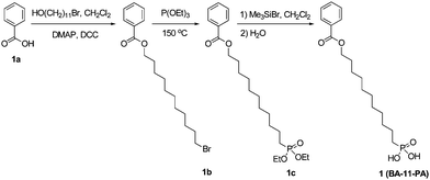
11-Bromoundecylbenzoate (1b)
To a solution of benzoic acid (0.977 g, 8.0 mmol) and 11-bromoundecanol (2.01 g, 8.0 mmol) in dry methylene chloride (20 mL) under nitrogen were added 4-dimethylaminopyridine (DMAP, 0.293 g, 2.4 mmol) and 1,3-dicyclohexylcarbodiimide (DCC, 2.15 g, 10.4 mmol). The mixture was stirred for 24 h at room temperature. The reaction mixture was filtered and washed with methylene chloride. The collected methylene chloride solution was dried with Na2SO4, and concentrated. The crude product was purified over a silica gel column chromatograph with hexane–methylene chloride (1![[thin space (1/6-em)]](https://www.rsc.org/images/entities/char_2009.gif) :1) as the eluent to afford a colorless liquid (2.06 g, 73%). 1H NMR (300 MHz, CDCl3): δ 8.01–8.07 (m, 2H), 7.40–7.56 (m, 3H), 4.32 (t, 2H, J = 6.9 Hz), 3.40 (t, 2H, J = 6.9 Hz), 1.28–1.88 (m, 18H). C18H27BrO2: calcd C 60.85, H 7.66, Br 22.49; found C 60.70, H 7.79, Br 22.57. ESI-MS (m/z): calcd 354.1; found 354.1.
:1) as the eluent to afford a colorless liquid (2.06 g, 73%). 1H NMR (300 MHz, CDCl3): δ 8.01–8.07 (m, 2H), 7.40–7.56 (m, 3H), 4.32 (t, 2H, J = 6.9 Hz), 3.40 (t, 2H, J = 6.9 Hz), 1.28–1.88 (m, 18H). C18H27BrO2: calcd C 60.85, H 7.66, Br 22.49; found C 60.70, H 7.79, Br 22.57. ESI-MS (m/z): calcd 354.1; found 354.1.
Diethyl-11-(phenylcarboxyl)undecylphosphonate (1c)
A mixture of 1b (1.24 g, 3.5 mmol) and triethyl phosphite (19.10 g, 114.9 mmol, 20.0 mL) was heated under nitrogen at 150 °C for 17 h. The excess of triethyl phosphite was removed by distillation under vacuum. The crude product was purified over a silica gel column chromatograph with methylene chloride to methylene chloride–ethyl acetate (1:1) as the eluents to afford a colorless liquid (1.27 g, 88%). 1H NMR (300 MHz, CDCl3): δ 8.01–8.07 (m, 2H), 7.40–7.56 (m, 3H), 4.31 (t, 2H, J = 6.9 Hz), 4.04–4.14 (m, 4H), 1.28–1.80 (m, 26H). C22H37O5P: calcd C 64.06, H 9.04, P 7.51; found C 63.92, H 9.20, P 7.44. ESI-MS (m/z): calcd 412.2; found 412.3.
Benzoic acid-11-phosphono-undecyl ester (BA-11-PA, 1)
To a solution of 1c (0.619 g, 1.5 mmol) in dry methylene chloride (15 mL) under nitrogen was dropwise added bromotrimethylsilane (1.38 g, 1.17 mL, 9.0 mmol). The mixture was stirred for 22 h at room temperature. The reaction mixture was poured into water (200 mL), filtered and washed with a large amount of water to afford a white solid (0.517 g, 97%). 1H NMR (300 MHz, CDCl3): δ 8.01–8.06 (m, 2H), 7.41–7.56 (m, 3H), 4.30 (t, 2H, J = 6.9 Hz), 1.28–1.82 (m, 20H). C18H29O5P: calcd C 60.66, H 8.20, P 8.69; found C 60.51, H 8.32, P 8.54. ESI-MS (m/z): calcd 356.2; found 356.1.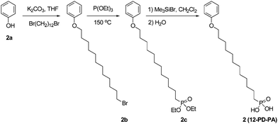
12-Bromododecoxybenzene (2b)
To a solution of phenol (1.88 g, 20.0 mmol) and 1,12-dibromododecane (6.56 g, 20.0 mmol) in dry THF (50 mL) under nitrogen was added potassium carbonate (4.15 g, 30.0 mmol). The mixture was stirred for 17 h under reflux, cooled down to room temperature and filtered to remove insoluble salts. The filtrate was concentrated by rotary evaporation under reduced pressure. The crude product was purified over a silica gel column chromatograph with hexane–methylene chloride (3:1) as the eluent to afford a white solid (4.17 g, 61%). 1H NMR (300 MHz, CDCl3): δ 7.24–7.31 (m, 2H), 6.87–6.96 (m, 3H), 3.95 (t, 2H, J = 6.6 Hz), 3.41 (t, 2H, J = 6.9 Hz), 1.27–1.89 (m, 20H). C18H29BrO: calcd C 63.34, H 8.56, Br 23.41; found C 63.19, H 8.65, Br 23.33. ESI-MS (m/z): calcd 340.1; found 340.2.
Diethyl-12-phenoxydodecylphosphonate (2c)
A mixture of 2b (1.28 g, 3.75 mmol) and triethyl phosphite (19.10 g, 114.9 mmol, 20.0 mL) was heated under nitrogen at 150 °C for 18 h. The excess of triethyl phosphite was removed by distillation under vacuum. The crude product was purified over a silica gel column chromatograph with methylene chloride to methylene chloride–ethyl acetate (1:1) as the eluents to afford a white solid (1.26 g, 85%). 1H NMR (300 MHz, CDCl3): δ 7.24–7.31 (m, 2H), 6.87–6.96 (m, 3H), 4.02–4.15 (m, 4H), 3.95 (t, 2H, J = 6.6 Hz), 1.26–1.81 (m, 28H). C22H39O4P: calcd C 66.30, H 9.86, P 7.77; found C 66.15, H 9.97, P 7.69. ESI-MS (m/z): calcd 398.3; found 398.3.
(12-Phenoxy-dodecyl)-phosphonic acid (12-PD-PA, 2)
To a solution of 2c (0.598 g, 1.5 mmol) in dry methylene chloride (15 mL) under nitrogen was dropwise added bromotrimethylsilane (1.38 g, 1.17 mL, 9.0 mmol). The mixture was stirred for 19 h at room temperature. The reaction mixture was poured into water (200 mL), filtered and washed with a large amount of water to afford a white solid (0.472 g, 92%). 1H NMR (300 MHz, CDCl3): δ 7.24–7.31 (m, 2H), 6.87–6.96 (m, 3H), 3.95 (t, 2H, J = 6.6 Hz), 1.27–1.81 (m, 22H). C18H31O4P: calcd C 63.14, H 9.13, P 9.05; found C 62.96, H 9.24, P 8.97. ESI-MS (m/z): calcd 342.2; found 342.2.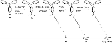
2-Triptycenylcarboxylic acid (6b)
2-Bromotriptycene (1.00 g, 3.0 mmol) was added to dry THF (10 mL) and cooled to −78 °C in a dry ice/acetone bath for 20 min. Tert-butyllithium (3.53 mL, 1.7 M in THF, 6.0 mmol) was added dropwise and the mixture was cooled for another 20 min. The mixture was then warmed up to 0 °C for 20 min and then re-cooled to −78 °C. After 20 min, CO2 (dry ice) was crushed and placed in a closed flask. The carbon dioxide gas was transferred via a needle and bubbled into the solution at −78 °C for 30 min. After bubbling, the cloudy mixture was acidified with 2 M HCl until the solution was acidic. The solution was removed, washed with water, extracted with ethyl acetate, and dried over sodium sulfate. Following evaporation in vacuo, the residue was purified over a silica gel column chromatograph with hexanes–ethyl acetate (10:1 to 6:1) as the eluent to afford a faint yellowish white solid (0.610 g, 68%). 1H NMR (500 MHz, DMSO-d6): δ 12.81 (broad s, 1H), 8.00 (s, 1H), 7.65 (d, 1H, J = 7.5 Hz), 7.55 (d, 1H, J = 7.5 Hz), 7.45 (m, 4H), 7.01 (m, 4H), 5.78 (s, 1H), 5.75 (s, 1H). 13C NMR (125 MHz, CDCl3): δ 27.1, 53.9, 54.1, 54.2, 123.7, 123.9, 125.1, 125.2, 125.5, 125.6, 126.2, 128.3, 144.2, 144.7, 145.3, 145.9, 151.5, 172.2. C21H14O2: calcd C 84.54, H 4.73; found C 84.41, H 4.84. ESI-MS (m/z): calcd 298.1; found 297.3.
1-(2-Triptycenylcarboxy)-12-bromododecane (6c)
To a solution of 6b (0.312 g, 1.05 mmol) and 12-bromododecanol (0.308 g, 1.16 mmol) in dry methylene chloride (20 mL) under nitrogen were added 4-(dimethylamino)pyridium-4-toluenesulfonate (DPTS, 88.3 mg, 0.30 mmol) and 1,3-dicyclohexylcarbodiimide (DCC, 0.402 g, 1.95 mmol). The mixture was stirred for 24 h at room temperature. The reaction mixture was filtered and washed with methylene chloride. The collected methylene chloride solution was dried with Na2SO4, and concentrated. The crude product was purified over a silica gel column chromatograph with hexane–methylene chloride (3:1 to 1:1) as the eluent to afford a slightly yellow viscous liquid (0.309 g, 54%). 1H NMR (300 MHz, CDCl3): δ 8.04 (s, 1H), 7.73 (d, 1H, J = 7.5 Hz), 7.39–7.46 (m, 5H), 6.98–7.03 (m, 4H), 5.51 (s, 1H), 5.49 (s, 1H), 4.25 (t, 2H, J = 6.6 Hz), 3.41 (t, 2H, J = 6.6 Hz), 1.22–1.95 (m, 20H). C33H37BrO2: calcd C 72.65, H 6.84, Br 14.65; found C 72.50, H 6.97, Br 14.59. ESI-MS (m/z): calcd 544.2; found 544.1.
Diethyl-12-(2-triptycenylcarboxy)dodecylphosphonate (6d)
A mixture of 6c (0.302 g, 0.55 mmol) and triethyl phosphite (9.55 g, 53.5 mmol, 10.0 mL) was heated under nitrogen at 150 °C for 18 h. The excess of triethyl phosphite was removed by distillation under vacuum. The crude product was purified over a silica gel column chromatograph with methylene chloride to methylene chloride–ethyl acetate (1:1) as the eluents to afford a white solid (0.189 g, 57%). 1H NMR (300 MHz, CDCl3): δ 8.04 (s, 1H), 7.73 (d, 1H, J = 7.5 Hz), 7.38–7.46 (m, 5H), 6.98–7.03 (m, 4H), 5.51 (s, 1H), 5.49 (s, 1H), 4.25 (t, 2H, J = 6.6 Hz), 4.05–4.15 (m, 4H), 1.24–1.96 (m, 28H). C37H47O5P: calcd C 73.73, H 7.86, P 5.14; found C 73.61, H 7.97, P 5.07. ESI-MS (m/z): calcd 602.3; found 602.2.
12-(2-Triptycenylcarboxy)dodecylphosphonic acid (Trip-12-PA, 6)
To a solution of 6d (0.183 g, 0.30 mmol) in dry methylene chloride (15 mL) under nitrogen was dropwise added bromotrimethylsilane (0.276 g, 0.23 mL, 1.80 mmol). The mixture was stirred for 28 h at room temperature. The reaction mixture was poured into water (200 mL), filtered and washed with a large amount of water to afford a white solid (0.151 g, 92%). 1H NMR (300 MHz, CDCl3): δ 8.04 (s, 1H), 7.73 (d, 1H, J = 7.5 Hz), 7.37–7.46 (m, 5H), 6.97–7.04 (m, 4H), 5.51 (s, 1H), 5.49 (s, 1H), 4.26 (t, 2H, J = 6.6 Hz), 1.25–1.98 (m, 22H). C33H39O5P: calcd C 72.51, H 7.19, P 5.67; found C 72.37, H 7.30, P 5.58. ESI-MS (m/z): calcd 546.3; found 546.3.Substrate preparation and AlOx formation
Heavily P-doped silicon substrates with 300 nm thermally grown oxide were cleaned by piranha etching H2SO4:H2O2 (3:1 by volume) for 10 minutes, followed by immersion in H2O:H2O2:NH4OH (5:1:1 by volume) and through rinsing in DI H2O. Clean substrates were placed in a Diener Femto low-pressure air plasma system for 10 minutes beneath an overhanging aluminum electrode operating at 40 kHz. This has been shown by our group to deposit a ∼2.5 nm thick layer of AlOx on substrate surfaces as previously verified by time of flight secondary ion mass spectroscopy (TOF-SIMS).48
Self-assembly and SAM cleaning
All self-assembly was carried out overnight (16 h) in 0.1 mM solutions under ambient conditions. For BA-11-PA, 12-PD-PA, PhO-19-PA, DDPA, and ODPA, tetrahydrofuran (THF) was used as a solvent. For Trip-12-PA, chloroform was used as a solvent.Once substrates were removed from their respective assembly solutions, the residual compound was removed by 10 min sonication in baths of clean solvent. BA-11-PA coated substrates were cleaned by sonication in 1:20 triethylammine (TEA):THF followed by that in THF and ethanol (EtOH). 12-PD-PA and PhO-19-PA were cleaned by sonication in 1:20 TEA:dimethylformamide (DMF), followed by that in THF and EtOH. DDPA and ODPA were cleaned by sonication in THF, then in hexanes. Trip-12-PA was cleaned by sonication in 1:20 TEA:chloroform, followed by that in chloroform and EtOH.
All self-assembly conditions employed here have been optimized such that the substrate surface post-assembly and cleaning has the highest possible water contact angle. In doing so, SAMs are qualitatively assessed to be dense, as any deviation from the highest measured value is indicative of exposed underlying oxide.
SAM surface characterization (AFM)
To ensure that the residual compound had been successfully removed from the substrate surface, SAMs were examined by atomic force microscopy (AFM). Images were taken in tapping mode using a Multimode Nanoscope III atomic force microscope made by Digital Instruments. Etched silicon tips with resonant frequencies between 300 and 350 kHz were used. Roughness measurements were conducted using NanoScope Analysis V1.20. Images of the pentacene grain morphology were also acquired in this way.Surface energy measurements and calculations
Surface energy was measured by contact angle goniometry utilizing the well-established Wu (harmonic mean) method. Diiodomethane (DIM) and deionized water were used as probe solvents. The contact angles of five droplets of DI H2O and diiodomethane were averaged to calculate dispersion and polar components. All measurements were in very good agreement with one another as no more than 3° in contact angle deviation was seen between any two measurements on the same SAM surface.SAM characterization (NEXAFS)
NEXAFS spectra were collected at the National Synchrotron Light Source (NSLS) U7A beamline at Brookhaven National Laboratory, which uses an elliptically polarized beam with about 85% p-polarization. For the experiments we used a monochromator with a 600 l mm−1 grating that provides a full-width at half-maximum (FWHM) resolution of ∼0.15 eV at the carbon K-edge (285 eV). The monochromator energy scale was calibrated using the 285.35 eV C 1s–π*(C![[double bond, length as m-dash]](https://www.rsc.org/images/entities/char_e001.gif) C) transition on a graphite transmission grid placed in the path of the X-rays.58 To suppress artifacts due to incident beam intensity variation and monochromator absorption features, the spectra were normalized by the spectrum of an upstream gold-coated mesh prepared by evaporation of gold in vacuo. Both the reference and signal were divided by the beam flux as a function of photon energy prior to normalization.59 Partial electron yield was monitored by a detector with the threshold voltage maintained at −150 V. Samples were mounted to allow rotation about the vertical axis to change the angle between the sample surface and the incident X-ray beam. The NEXAFS angle is defined as the angle between the incident X-ray beam and the sample surface.
C) transition on a graphite transmission grid placed in the path of the X-rays.58 To suppress artifacts due to incident beam intensity variation and monochromator absorption features, the spectra were normalized by the spectrum of an upstream gold-coated mesh prepared by evaporation of gold in vacuo. Both the reference and signal were divided by the beam flux as a function of photon energy prior to normalization.59 Partial electron yield was monitored by a detector with the threshold voltage maintained at −150 V. Samples were mounted to allow rotation about the vertical axis to change the angle between the sample surface and the incident X-ray beam. The NEXAFS angle is defined as the angle between the incident X-ray beam and the sample surface.
Pentacene device fabrication and characterization
Although self-assembly and SAM cleaning were performed under ambient conditions, once complete, substrates were placed in a dry N2 glovebox environment containing a thermal evaporator (Angstrom Engineering)/probe station and were never again exposed to air. Segregated regions of pentacene were thermally evaporated onto the various SAM surfaces at a rate of 0.2 Å s−1 for a final thickness of 40 nm and were patterned by a shadow mask. During evaporation substrates were held at a constant temperature of 60 °C; once complete, substrates were kept under high vacuum and allowed to cool to room temperature overnight. Gold source and drain electrodes were patterned by a shadow mask and evaporated at 1 Å s−1 for a final thickness of 50 nm.Pentacene devices were characterized in a dry N2 environment using an Agilent 4155B semiconductor parameter analyzer. Field effect mobility (μ) was calculated in the saturation regime using a linear fit of (−Ids)1/2vs. Vgs. The threshold voltage (Vt) was calculated as the x-intercept of the linear section of the (Ids)1/2versus Vgs plot. Subthreshold swing (S) was calculated by the inverse slope of Idsversus Vgs in the region of exponential current increase. All devices measured had a channel length of 12 μm and a width of 1000 μm. At least 20 devices were measured on each SAM surface spreading over multiple substrates.
Results and discussion
Rationale of the SAM molecular design
To elicit a true structure–property relationship between the SAM structure and device performance, a dielectric platform must be carefully chosen to eliminate effects of extraneous variables such as surface roughness, Fröhlich polaron formation, and sites of nucleation such as grain boundaries.47 For these reasons our dielectric layer was chosen to be 300 nm thermally grown silicon oxide (0.2 nm RMS roughness) on a P-doped Si wafer. To promote binding of PA SAMs, a 2 nm AlOx layer was deposited on the surface of SiO2via a plasma enhanced deposition process. This dielectric platform has been extensively studied by our group and is an excellent way to research PA assembly as the surface post-AlOx plasma deposition is continuous, morphologically identical to the underlying Si, and readily reactive with PA under ambient conditions.12,48 Using this basic architecture, the following PA SAM molecules were chosen to study pentacene devices: benzoic acid-11-phosphono-undecyl ester (BA-11-PA), (12-phenoxy-dodecyl)-phosphonic acid (12-PD-PA), dodecyl-phosphonic acid (DDPA), [8-(11-phenoxy-undecyloxy)-octyl]-phosphonic acid (PhO-19 PA), octadecyl-phosphonic acid (ODPA), and 12-(2-triptycenylcarboxy)dodecylphosphonic acid (Trip-12-PA) (Fig. 1). From systematic examination of the SAM structure–pentacene property relationship, we propose dominant mechanisms for optimal pentacene grain growth and charge transport properties.![Molecular structures of all six SAMs used in this study. (1) Benzoic acid-11-phosphono-undecyl ester (BA-11-PA), (2) (12-phenoxy-dodecyl)-phosphonic acid (12-PD-PA), (3) dodecyl-phosphonic acid (DDPA), (4) [8-(11-phenoxy-undecyloxy)-octyl]-phosphonic acid (PhO-19-PA), (5) octadecyl-phosphonic acid (ODPA), and (6) 12-(2-triptycenylcarboxy)dodecylphosphonic acid (Trip-12-PA).](/image/article/2013/TC/c2tc00378c/c2tc00378c-f1.gif) | ||
| Fig. 1 Molecular structures of all six SAMs used in this study. (1) Benzoic acid-11-phosphono-undecyl ester (BA-11-PA), (2) (12-phenoxy-dodecyl)-phosphonic acid (12-PD-PA), (3) dodecyl-phosphonic acid (DDPA), (4) [8-(11-phenoxy-undecyloxy)-octyl]-phosphonic acid (PhO-19-PA), (5) octadecyl-phosphonic acid (ODPA), and (6) 12-(2-triptycenylcarboxy)dodecylphosphonic acid (Trip-12-PA). | ||
As previously mentioned, all SAM molecules were rationally designed to probe specific aspects of monolayer structural order, surface homogeneity and surface energy. SAMs with similar surface energy but different structural order were used to decipher the dominant effects on pentacene nucleation, growth, and device performance. For example, if SAM structural order effects are dominant, a small substitution made to the terminal moiety of a predominantly alkyl SAM should have minimal impact on device performance. However, if surface energy is a dominant mechanism, the alkyl-chain length should play a trivial role in device performance and substitution made to the terminal moiety would be highly impactful.
DDPA and ODPA were chosen for their comparable low surface energies, yet different structural orders. DDPA is less-ordered and liquid-like, whereas ODPA has been shown to be highly ordered existing in an all-trans conformation when densely assembled. Similarly, 12-PD-PA and PhO-19-PA were chosen for their comparable mid-level surface energy, yet very different structural order. 12-PD-PA is less-ordered/liquid-like whereas PhO-19-PA's long alkyl-chain promotes a ridged crystalline SAM. BA-11-PA and Trip-12-PA were chosen for their comparable higher surface energy, but large difference in the SAM surface texture. While BA-11-PA results in a molecularly smooth liquid-like surface (similar to DDPA and 12-PD-PA), Trip-12-PA's three-pronged terminal moiety facilitates a disordered and “molecularly rough” SAM surface.
Surface energy calculations and characterization of SAMs by AFM
Surface energies of all SAMs were measured via contact angle goniometry using the Wu model (harmonic mean) to calculate both dispersive (γd) and polar (γp) components of total surface energy (γtotal) (Table 1).49,50 It should be noticed that many of the molecules in this study were designed to have similar surface energies but different structural order once assembled. Both alkyl-PA monolayers of DDPA and ODPA have similar and exceptionally low surface energies relative to the other SAM structures but have different alkyl-chain lengths. Similarly, PhO-19-PA and 12-PD-PA SAMs have comparable (although higher) surface energy values to each other, yet differ greatly in their chain lengths. BA-11-PA SAM exhibits a slightly higher surface energy still, but is comparable in structure to 12-PD-PA. The triptycene-based SAM of Trip-12-PA exhibits similar surface energy to BA-11-PA but differs in molecular-scale surface homogeneity due to the presence of a large three-dimensional terminal moiety.| SAM | Avg. θ water [°] | Avg. θ DIM [°] | γ polar [mN m−1] | γ dispersive [mN m−1] | γ total [mN m−1] |
|---|---|---|---|---|---|
| BA-11-PA | 69.2 | 33.6 | 12.7 | 43.0 | 55.7 |
| 12-PD-PA | 82.0 | 38.6 | 7.5 | 40.8 | 48.3 |
| DDPA | 107.1 | 69.4 | 1.1 | 25.8 | 26.8 |
| PhO-19-PA | 79.7 | 38.1 | 8.4 | 41.0 | 49.4 |
| ODPA | 110.3 | 69.1 | 0.03 | 26.0 | 26.1 |
| Trip-12-PA | 68.8 | 37.1 | 13.2 | 41.5 | 54.6 |
| Bare AlOx | 12.0 | 36.5 | 37.7 | 41.7 | 79.4 |
AFM images obtained of these monolayers show SAM coated surfaces that are almost morphologically identical (Fig. 2). No boundaries or defects can be resolved in the images and all substrates have a very similar surface roughness of 0.20–0.30 nm RMS, which is comparable to that of bare SiO2.
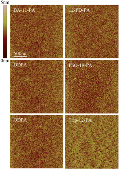 | ||
| Fig. 2 AFM images of the SAM coated substrate morphology. All substrates exhibit similar roughness to bare SiO2 coated with a 2.5 nm AlOx adhesion layer (0.25 nm RMS). Note that no surface aggregation is seen on any of the surfaces, indicative of true monolayer formation. | ||
Spectral characterization of SAMs by NEXAFS
Structural characterization of the SAM molecules adhered to the AlOx coated substrate was carried out through near edge X-ray absorption fine structure spectroscopy, yielding both qualitative assessment of the structural order and average tilt angle associated with various moieties. C K-edge spectra of the PA SAMs, collected at an X-ray incidence angle of 55°, can be found in Fig. 3. At an incident angle of 55°, the spectra are independent of orientation effects (the so-called magic angle of NEXAFS).51 All spectra show characteristic absorption resonances at ∼287.7 eV (R*/C–H σ*) and ∼293.3 eV related to the aliphatic carbon chains (C–C σ*).52,53 Trip-12-PA, PhO-19-PA, BA-11-PA and 12-PD-PA show an additional pronounced pre-edge feature near 285 eV associated with the terminal aromatic rings (CC π*).52 Trip-12-PA and BA-11-PA also exhibit a C 1s–CO resonance near 288.5 eV related to the ester moieties.51,54 For the other SAMs no features related to CO containing species, which are common contaminants in SAMs, were detected.
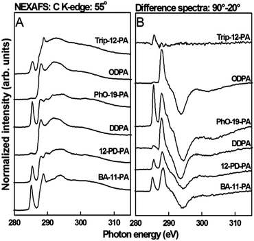 | ||
| Fig. 3 Near-edge X-ray absorption fine structure (NEXAFS) spectra taken of all SAMs used in this study. (A) Carbon K-edge spectra collected at 55° and (B) 90–20° difference spectra. | ||
NEXAFS difference spectra for 90° and 20° X-ray incidence angles can be found in the right panel of Fig. 3. The Trip-12-PA SAMs showed almost no dichroism and the film is mostly disordered. We will exclude Trip-12-PA from the following discussion of structural parameters. All other SAMs showed an angle dependence (i.e. difference spectra intensity) for the C–H and C–C related peaks, a clear indication that a well-defined monolayer was formed. Molecular orbitals related to the R* transition (C–H) are oriented perpendicular to the alkyl chain axis while those related to transitions into the C–C and C–C′ σ* orbitals are oriented parallel to the chain axis.51 The polarity of the difference peaks thus proves that the alkane chains are in an upright orientation. The π* resonances of BA-12-PA, 12-PD-PA and PhO-19-PA exhibited positive dichroisms signifying upright phenyl ring orientations.
For a more quantitative picture of the general PA SAM structure on AlOx, the tilt angle of the n-alkyl chains and the ring structures for the most ordered SAM, PhO-19-PA, was determined from the dichroisms at the R* and π* resonances, respectively. The intensities of these resonances as a function of the X-ray incidence angle are evaluated for spectra collected at 90°, 70°, 55°, 30° and 20° using published procedures.51 From these data the average tilt angle was found to be 27 ± 5.0° for the alkyl chain and 66 ± 5.0° for the plane normal to the phenyl ring against the surface normal. This is in good agreement with the chain orientation found for PA SAMs on HfOx, Ag and SiOx.
Differences in SAM order and alignment were quantified by analyzing the NEXAFS dichroic ratio:
| ΔN = (N90° − N20°)/(N90° + N20°) | (1) |
C π*) are summarized in Table 2. For the chain order, there is a clear increase in molecular alignment going from shorter to longer alkane chains; the ΔN values increase by nearly 25% for the long-chain SAMs. The chain order also has significant impact on the alignment of the terminal groups. For the phenyl moieties the order parameter ΔN increases three-fold going from any short-chain SAMs with mostly disordered phenyl units to the long-chain PhO-19-PA film with a ΔN of 0.30. In conclusion, while most SAMs studied here are generally well-defined films with a mostly upright orientation of the alkane and phenyl units, the order of the films was strongly dependent on the chain length. Shorter chains lead to a more disordered amorphous SAM structure, due to defects in the alkyl-chains.
To simplify interpretation of these data, SAMs used in this study are arranged into three groups based on the alkyl-chain dichroic ratio: disordered (Trip-12-PA), less ordered (BA-11-PA, 12-PD-PA, DDPA), and more ordered (ODPA, PhO-19-PA). This will become important when discussing the relationship between the SAM structure and device performance (Scheme 2).
Examination of the pentacene morphology by AFM
Pentacene was thermally evaporated onto the SAM coated substrate surfaces to form the organic semiconducting layer of OFET device architecture. High mobility pentacene OFETs are typically characterized by large interdigitated dendritic crystals.23 In Fig. 4 the largest pentacene grains of this type are exhibited by SAMs of BA-11-PA, 12-PD-PA and DDPA. Conversely, pentacene films grown on SAMs comprised of long alkyl chains ∼(CH2)18 or longer are shown to have small boxy grains. Although the triptycene-based SAM has roughly the same alkyl chain length as BA-11-PA, 12-PD-PA and DDPA, the observed pentacene grain size is much smaller than any of these structures.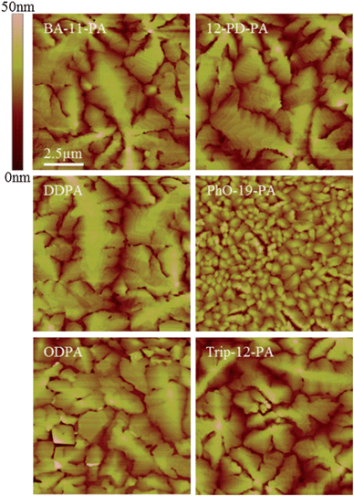 | ||
| Fig. 4 AFM images of 40 nm thick pentacene films evaporated on SAM surfaces. Large dendritic grains can be seen on SAMs of BA-11-PA, 12-PD-PA, and DDPA, relative to the other three SAMs. | ||
Nucleation and growth kinetics of monolayer pentacene can be used to explain the morphology seen in Fig. 4. It is known that the nucleation density of adsorbed pentacene molecules (N) is proportional to the deposition rate (F) divided by surface diffusion constant (D): N ≈ F/D. As F is held at 0.2 Å s−1, the diffusion constant governs the growth process.55 For alkyl-SAMs of length ≥(CH2)16 monolayers exhibit a highly ordered crystalline structure in which bonds are in an all trans-conformation. During the self-assembly process, grains between regions of highly ordered SAMs are formed. This results in monolayer grain boundary defects on the surface acting as sites of pentacene nucleation, decreasing the surface diffusion constant and increasing the nucleation density. Mid-length disordered alkyl-SAM surface morphology can be compared to a liquid, reducing the impact of SAM grain boundaries. This eliminates potential sites for pentacene nucleation and decreases nucleation density.23,56
SAMs of BA-11-PA and 12-PD-PA facilitate large pentacene grain growth through this liquid-like surface mechanism, as pentacene thin films on these molecular structures are observed to have a similar grain size and structure to those of DDPA. This demonstrates that the SAM terminal moiety has a degree of synthetic flexibility and allows for tunable surface energy without compromising device performance. PhO-19-PA and ODPA SAM surfaces exhibit much smaller pentacene grain growth consistent with the SAM grain boundary mechanism. The Trip-12-PA SAM has a liquid-like/disordered surface but results in a small pentacene grain structure. Though this may seem counterintuitive, further explanation will be given in the section “Pentacene device performance and SAM surface homogeneity relationship.”
Pentacene thin film transistor device performance
Pentacene thin film transistors were fabricated by evaporating 50 nm thick Au electrodes onto segregated regions of 40 nm thick pentacene (Scheme 1). Characteristic output and transfer curves for devices on all six SAM surfaces can be found in Fig. 5 and 6, and summarized device performance specifications for all measured FETs can be found in Table 3. From the data presented in Table 3 it can be clearly seen that substrates coated with BA-11-PA, 12-PD-PA and DDPA SAMs exhibit significantly higher device performance than the other SAMs used in this study, achieving charge carrier mobilities up to 4.1 cm2 V−1 s−1. It should be noted that longer SAM molecules of comparable surface energy and structure exhibit device performance that is inferior. Dielectrics coated with PhO-19-PA, which has comparable surface energy and similar structure to 12-PD-PA, show much smaller pentacene grains and mobility measurements approximately 75% lower. ODPA exhibited mobility measurements comparable to/slightly higher than those achieved in previous studies, yet three times lower than those of DDPA.60 The triptycene-based SAM of Trip-12-PA, which has a comparable chain length and surface energy to the BA-11-PA molecule, exhibited the worst device performance among all SAM structures.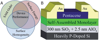 | ||
| Scheme 1 (A) Interplay of three SAM surface factors that lead to dictate pentacene device performance. (B) Pentacene FET device architecture. From bottom: a heavily P-doped Si wafer with 300 nm thermally grown SiO2, 2.5 nm plasma deposited AlOx layer, self-assembled monolayer, 40 nm thick thermally evaporated pentacene, 50 nm thick thermally evaporated Au source and drain electrodes. Both pentacene and electrodes patterned by a shadow mask. | ||
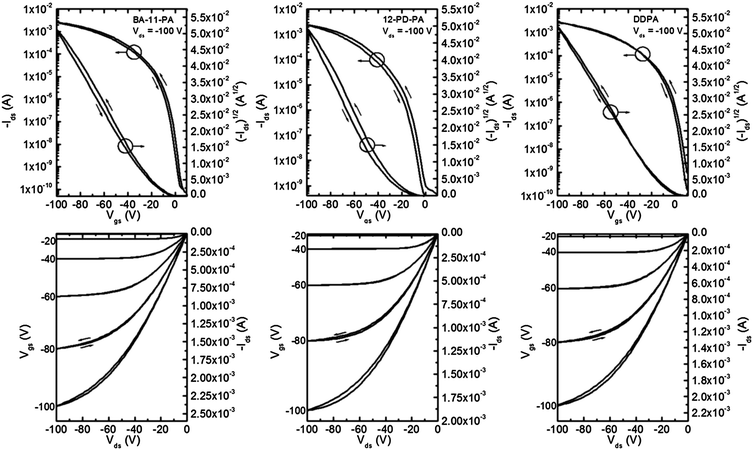 | ||
| Fig. 5 Representative transfer and output curves for pentacene devices fabricated on BA-11-PA, 12-PD-PA and DDPA SAMs. Channel length 12 μm, channel width 1000 μm. | ||
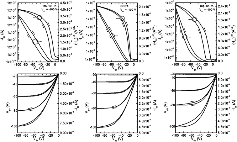 | ||
| Fig. 6 Representative transfer and output curves for pentacene devices fabricated on PhO-19-PA, ODPA and Trip-12-PA SAMs. Channel length 12 μm and channel width 1000 μm. | ||
| SAM | μ (cm2 V−1 s−1) (high) avg. ± avg. dev. | V t (V) avg. ± avg. dev. | S (V per decade) avg. ± avg. dev. | I on/Ioff highest–lowest |
|---|---|---|---|---|
| BA-11-PA | (4.0) 3.5 ± 0.28 | 26.0 ± 12.3 | 5.9 ± 2.4 | 3.2 × 10⁷ to 1.0 × 10⁶ |
| 12-PD-PA | (3.4) 3.15 ± 0.31 | 14.0 ± 7.3 | 4.3 ± 1.1 | 2.8 × 10⁷ to 2.2 × 10⁶ |
| DDPA | (4.1) 3.51 ± 0.39 | 18.6 ± 3.8 | 4.6 ± 2.2 | 5.0 × 10⁷ to 4.1 × 10⁶ |
| PhO-19-PA | (0.92) 0.91 ± 0.04 | 22.5 ± 7.5 | 4.0 ± 0.3 | 1.3 × 10⁷ to 6.9 × 10⁶ |
| ODPA | (1.3) 0.98 ± 0.21 | 27.4 ± 6.8 | 4.6 ± 2.2 | 1.1 × 10⁷ to 2.8 × 10⁶ |
| Trip-12-PA | (0.74) 0.51 ± 0.15 | 42.1 ± 6.7 | 9.2 ± 1.9 | 4.0 × 10⁶ to 5.0 × 10⁴ |
| Bare AlOx | (0.31) 0.23 ± 0.12 | 33.8 ± 9.5 | 16.7 ± 3.2 | 2.5 × 10⁵ to 4.2 × 10⁴ |
When comparing charge mobility values presented here it is important to keep in mind typical values for pentacene FET devices fabricated on unmodified oxide dielectrics. Measurements of 0.1–0.3 cm2 V−1 s−1 are commonly observed in our research group for this surface and are accompanied by large hysteresis and threshold voltage values (Table 3). As shown here, with a properly chosen SAM molecular structure, 15–20 times higher charge carrier mobility can be achieved in conjunction with low threshold voltage and minimal hysteresis.
From these results, two trends can be identified. First, devices in which dielectrics have been coated with SAMs possessing non-bulky terminal groups and the alkyl chain of ∼(CH2)12 exhibit much higher pentacene charge carrier mobility in comparison to bulky or long SAMs. Second, surface energy appears to be randomly correlated with pentacene growth and charge carrier mobility.
Pentacene device performance and SAM structural order relationship
In the previous literature many claims have been made about how the SAM molecular structure influences pentacene device performance. In previous papers SAMs with a high degree of crystallinity were desired to promote high-quality device performance.57 As mentioned in the section “Examination of pentacene morphology by AFM,” mid-length ∼(CH2)12 alkyl-monolayers (DDPA) exist in a liquid-like disordered state promoting high mobility device performance.23,56 In this liquid form, molecules are not aligned in a perfect all-trans-conformation, and therefore variations in orientation and meeting of two grains do not affect the SAM surface. It is shown here that this same principle also applies to alkyl-type SAMs modified with different non-bulky terminal groups. The BA-11-PA and 12-PD-PA SAM structures used in this study are shown to be similarly amorphous to DDPA from NEXAFS (Fig. 3) and facilitate the construction of pentacene devices with comparable performance (Fig. 5 and Table 3). Since the alkyl chains present in these SAM structures are both mid-length-disordered, and the phenyl terminal group is not large enough to promote strong π–π stacking, a disordered surface ideal for pentacene grain growth is formed. This is highly advantageous from a processing standpoint and will be addressed more in the section “Pentacene device performance and SAM surface energy relationship.”For PhO-19-PA and ODPA, grain boundaries are present in the crystalline SAM layer promoting small pentacene crystals and reduced charge carrier mobility. When comparing these two structures, pentacene grains are found to be even smaller on the PhO-19-PA SAM, which possesses a longer alkyl chain structure.
Pentacene device performance and SAM surface homogeneity relationship
A corollary of the SAM structure resulting in a smooth surface is the concept of surface homogeneity, defined here as “uninterrupted surface periodicity.” In highly ordered (crystalline) SAM structures (PhO-19-PA, ODPA) it can be hypothesized that boundaries between regions of high density SAMs result in molecular scale defects/monolayer grain boundaries. During self-assembly, as sites of monolayer nucleation grow and coalesce, grain boundaries form. Boundaries can best be described as the meeting point of two chemically identical monolayers of different structural orientation and are analogous to classic metallic grains, albeit in two dimensions. These boundaries act as sites of pentacene nucleation, resulting in smaller pentacene grain growth and reduced charge mobility. Mid-length [∼(CH2)12] simple alkyl-based SAM structures do not allow for these sites of nucleation to exist because their surface structure is liquid-like. As enthalpic gain from van der Waals forces is not sufficient to overwhelm randomization of the SAM molecules, there is no periodicity to the mid-length-SAM surface structure and therefore long-range homogeneity cannot be disrupted.From Fig. 4 it can be seen that SAM molecules (BA-11-PA, 12-PD-PA, and DDPA) with mid-length disordered alkyl-chains promote the growth of very large dendritic pentacene grains, most of them exceeding 10 μm. Pentacene crystals of this type are known to allow for high mobility measurements due to the lack of grain boundaries impeding the motion of charge carriers.23a,b Conversely, highly crystalline SAMs of ODPA and PhO-19-PA resulted in the growth of small boxy grains (1–4 μm and 0.5–3 μm respectively) relative to the shorter structures. Discrepancy in the grain size between these two SAMs also manifests itself in device performance in which ODPA exhibits slightly higher mobility measurements than PhO-19-PA, albeit both exhibit far worse performance than the previously mentioned shorter structures. As large (>10 μm) grains only occurred in less-ordered mid-length SAM molecular structures, the principle of surface homogeneity set forth here is further validated.
For continued testing of this hypothesis, Trip-12-PA was synthesized. The alkyl chain is disordered and the SAM is liquid-like in nature (Fig. 3), but due to the three-dimensional terminal group of triptycene, there will always be molecular-scale dips and peaks in this SAM surface akin to a SAM grain boundary or gauche defects in ordered structures. Accordingly, the pentacene grain size is small relative to the other short molecules (1–7 μm compared to >10 μm) (Fig. 4), and charge mobility and Ion/Ioff ratio measurements are much lower on this platform than all other SAM structures (Fig. 6 and Table 3). It should be noted, however, that the pentacene grain size on Trip-12-PA is not as small as ODPA or PhO-19-PA yet it exhibits inferior performance. We believe that this is due to the molecularly rough surface impeding charge transfer in the first few molecular layers, yet sometimes not providing enough of a dip or valley to induce nucleation (allowing for the large deviation in the grain size seen).
Although not shown, pentacene grown on the bare oxide results in small boxy grains exhibiting poor OFET performance; presumably attributed to both charge traps and high grain boundary density.
Pentacene device performance and SAM surface energy relationship
Little correlation is observed between pentacene charge mobility and SAM surface energy. For molecules used in this study, liquid-like SAMs of BA-11-PA, 12-PD-PA and DDPA with surface energies ranging from 26.8–55.7 mN m−1 have shown similar high performance to one another, and much better performance than highly ordered SAMs of PhO-19-PA and ODPA with different energies (Tables 1 and 3 and Scheme 2). Although previous studies have tried to show a direct causal relationship between surface energy and pentacene device performance, this is not the case here. From the observed experimental results, if a SAM promotes a structurally homogeneous surface, while achieving sufficient density to block all charge traps, the dielectric will provide a high-quality platform for semiconductor nucleation and growth.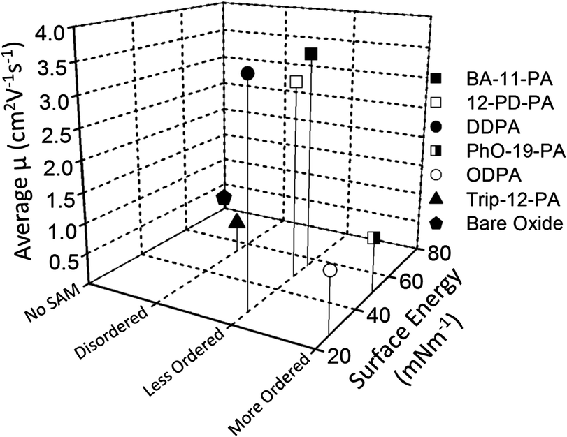 | ||
| Scheme 2 Plot of surface energy (X-axis), SAM alkyl-chain order established by dichroic ratio (Y-axis), and charge carrier mobility of pentacene OFET device (Z-axis) of all six SAM structures and bare AlOx/SiO2. | ||
Similarly, Mark's group found that for polymer dielectrics, surface chemical characteristics and surface energy play a trivial role in influencing pentacene growth and subsequent FET device performance, yet polymer surface microstructural mobility greatly affected experimental results.61
Although vacuum deposited pentacene was used in this systematic study for statistical reproducibility, the aforementioned observation is highly impactful in the context of organic device mass production. As surface energy of SAM structures employed to modify dielectric materials approach very low values such as those of DDPA and ODPA SAMs, techniques for solution processing of the semiconducting layer become limited. For instance, spin coating polymers/small molecules on alkyl-SAM surfaces are often not reproducible due to the solvent, and subsequently the organic semiconductor, de-wetting the surface leading to inconstant coverage. This same problem can be observed with dip coating organic semiconductors on hydrophobic substrates. For these types of solution processing, a SAM with mid-level surface energy and an amorphous structural nature is highly desirable (such as BA-11-PA or 12-PD-PA).
Conclusions
This study represents a major advancement in understanding the mechanisms at play between SAMs and linear organic semiconducting molecules. A systematic examination of six self-assembled monolayer structures was carried out to better define the relationship between the SAM molecular design and pentacene device performance. High charge carrier mobility pentacene OFET devices are demonstrated utilizing self-assembly to promote favorable pentacene nucleation and growth. Charge carrier mobilities of > 4.0 cm2 V−1 s−1 are observed for less ordered molecular SAM structures with non-bulky methyl-/phenyl-terminal groups and alkyl chains of ∼(CH2)12. The relationship between SAM surface homogeneity and pentacene device performance is probed using NEXAFS, contact angle goniometry and atomic force microscopy. It is concluded that if a SAM promotes a homogenous liquid-like surface with uninterrupted periodicity, achieved here through the use of mid-length alkyl-phenyl and methyl structures, pentacene device performance will be optimized. However, the terminal group should be carefully chosen to still allow for a molecularly smooth surface that does not disrupt surface homogeneity. To further validate this conclusion, a triptycene-terminated phosphonic acid molecule with a short alkyl chain was synthesized. Due to the ridged “pronged” nature of the triptycene moiety, surface homogeneity is never preserved regardless of terminal group orientation, and molecular valleys and peaks are formed after dense assembly. Accordingly, pentacene device performance on this SAM surface is greatly impeded.A variety of SAM structures with a wide range of surface energies were used in this study, and surface energy was examined with respect to pentacene device performance. It was found that surface energy tends to be a negligible factor in device performance provided that the aforementioned conditions for surface homogeneity are met (Scheme 2). This is promising for realizing integration of organic semiconductor devices into mass production, as the mid-level surface energy of phenyl-terminated amorphous SAM structures could potentially provide the platform for reproducible solution processing of high-performance OFETs.
Acknowledgements
This work is supported by the NSF-STC program under DMR-0120967 and the AFOSR program under FA9550-09-1-0426. T.W. and J.E.B. thank David Castner and NESAC/BIO (University of Washington) under NIH EB-002027 for supporting this work, as well as Daniel Fischer and Cherno Jaye (NIST) for providing the experimental equipment for NEXAFS spectroscopy and their help at the synchrotron. NEXAFS studies were performed at the NSLS, Brookhaven National Laboratory, which is supported by the U.S. Department of Energy, Division of Materials Science and Division of Chemical Sciences. A. K. Y. Jen thanks the World Class University (WCU) program through the National Research Foundation of Korea under the Ministry of Education, Science and Technology (R31-10035). Part of this work was conducted at the University of Washington NanoTech User Facility, a member of the NSF National Nanotechnology Infrastructure Network (NNIN).Notes and references
-
(a) D. J. Gundlach, Nat. Mater., 2006, 6, 173 CrossRef
; (b) T. N. Jackson, Nat. Mater., 2005, 6, 581 CrossRef
- L. Zhou, A. Wanga, S. C. Wu, J. Sun, S. Park and J. N. Thomas, Appl. Phys. Lett., 2006, 88, 083502 CrossRef
- M. Muccini, Nat. Mater., 2006, 5, 605 CrossRef CAS
- S. R. Forrest, Nature, 2004, 428, 911 CrossRef CAS
-
C. Kittel, in Introduction to Solid State Physics, ed. S. Johnson, John Wiley & Sons, Inc, Hoboken, NJ, 2005 Search PubMed
-
(a) H. Sirringhaus, Adv. Mater., 2005, 17, 2411 CrossRef CAS
- J. L. Bredas, D. Beljonne, V. Coropceanu and J. Cornil, Chem. Rev., 2004, 104, 4971 CrossRef CAS
-
(a) H. Ma, H. L. Yip, F. Huang and A. K. Y. Jen, Adv. Funct. Mater., 2010, 20, 1371 CrossRef CAS
- C. R. Newman, C. D. Frisbie, D. A. da Silva Filho, J.-L. Bredas, P. C. Ewbank and K. R. Mann, Chem. Mater., 2004, 16, 4436 CrossRef CAS
- G. Giri, E. Verploegen, S. C. B. Mannsfeld, S. Atahan-Evrenk, D. H. Kim, S. Y. Lee, H. A. Becerril, A. Aspuru-Guzik, M. F. Toney and Z. Bao, Nature, 2011, 480, 504 CrossRef CAS
- H. Li, B. C. K. Tee, J. J. Cha, Y. Cui, J. W. Chung, S. Y. Lee and Z. Bao, J. Am. Chem. Soc., 2012, 134, 2760 CrossRef CAS
- D. O. Hutchins, O. Acton, T. Weidner, N. Cernetic, J. E. Baio, G. Ting, D. G. Castner, H. Ma and A. K. Y. Jen, Org. Electron., 2012, 13, 464 CrossRef CAS
- M. Defaux, F. Gholamrezaie, J. Wang, A. Kreyes, U. Ziener, D. V. Anokhin, D. A. Ivanov, A. Moser, A. Neuhold, I. Salzmann, R. Resel, D. M. de Leeuw, S. C. J. Meskers, M. Moeller and A. Mourran, Adv. Mater., 2012, 24, 973 CrossRef CAS
- E. C. P. Smits, S. G. J. Mathijssen, P. A. van Hal, S. Setayesh, T. C. T. Geuns, K. A. H. A. Mutsaers, E. Cantatore, H. J. Wondergem, O. Werzer, R. Resel, M. Kemerink, S. Kirchmeyer, A. M. Muzafarov, S. A. Ponomarenko, B. de Boer, P. W. M. Blom and D. M. de Leeuw, Nature, 2008, 455, 956 CrossRef CAS
- M. Novak, A. Ebel, T. Meyer-Friedrichsen, A. Jedaa, B. F. Vieweg, G. Yang, K. Voitchovsky, F. Stellacci, E. Spiecker, A. Hirsch and M. Halik, Nano Lett., 2010, 11, 156 CrossRef
- O. Acton, G. G. Ting II, H. Ma, D. Hutchins, Y. Wang, B. Purushothaman, J. E. Anthony and A. K.-Y. Jen, J. Mater. Chem., 2009, 19, 7929 RSC
- G. G. Ting, O. Acton, H. Ma, J. W. Ka and A. K.-Y. Jen, Langmuir, 2009, 25, 2140 CrossRef CAS
- O. Acton, I. Osaka, G. Ting, D. O. Hutchins, H. Ma, R. D. McCullough and A. K. Y. Jen, Appl. Phys. Lett., 2009, 95, 113305 CrossRef
- P. Thissen, M. Valtiner and G. Grundmeier, Langmuir, 2009, 26, 156 CrossRef
- E. P. Gusev, E. Cartier, D. A. Buchanan, M. Gribelyuk, M. Copel, H. Okorn-Schmidt and C. D'Emic, Microelectron. Eng., 2001, 59, 341 CrossRef CAS
-
(a)
V. E. Henrich, The Surface Science of Metal Oxides, Cambridge University Press, Cambridge, UK, 1994 Search PubMed
- S. A. DiBenedetto, A. Facchetti, M. A. Ratner and T. J. Marks, Adv. Mater., 2009, 21, 1407 CrossRef CAS
-
(a) O. Acton, G. G. Ting, P. J. Shamberger, F. S. Ohuchi, H. Ma and A. K.-Y. Jen, ACS Appl. Mater. Interfaces, 2010, 2, 511 CrossRef CAS
- M. Dubey, T. Weidner, L. J. Gamble and D. G. Castner, Langmuir, 2010, 26, 14747 CrossRef CAS
- M. Halik, H. Klauk, U. Zschieschang, G. Schmid, C. Dehm, M. Schutz, S. Maisch, F. Effenberger, M. Brunnbauer and F. Stellacci, Nature, 2004, 431, 963 CrossRef CAS
- M. Halik and A. Hirsch, Adv. Mater., 2011, 23, 2689 CrossRef CAS
- C. D. Bain and G. M. Whitesides, Science, 1988, 240, 62 CAS
- T. Weidner, N. Ballav, U. Siemeling, D. Troegel, T. Walter, R. Tacke, D. G. Castner and M. Zharnikov, J. Phys. Chem. C, 2009, 113, 19609 CAS
- D. M. Jaffey and R. J. Madix, Surf. Sci., 1994, 311, 159 CrossRef CAS
- D. M. Jaffey and R. J. Madix, J. Am. Chem. Soc., 1994, 116, 3020 CrossRef CAS
- S. Savard, L. P. Blanchard, J. Léonard and R. E. Prud'homme, Polym. Compos., 1984, 5, 242 CrossRef CAS
- M. Wang, K. M. Liechti, Q. Wang and J. M. White, Langmuir, 2005, 21, 1848 CrossRef CAS
- C. R. Kessel and S. Granick, Langmuir, 1991, 7, 532 CrossRef CAS
- J. Randon, P. Blanc and R. Paterson, J. Membr. Sci., 1995, 98, 119 CrossRef CAS
- Y. Yee-Chia, K. Tsu-Jae and H. Chenming, Electron Devices, 2003, 50, 1027 CrossRef
-
K. Mistry, C. Allen, C. Auth, B. Beattie, D. Bergstrom, M. Bost, M. Brazier, M. Buehler, A. Cappellani, R. Chau, C. H. Choi, G. Ding, K. Fischer, T. Ghani, R. Grover, W. Han, D. Hanken, M. Hattendorf, J. He, J. Hicks, R. Huessner, D. Ingerly, P. Jain, R. James, L. Jong, S. Joshi, C. Kenyon, K. Kuhn, K. Lee, H. Liu, J. Maiz, B. McLntyre, P. Moon, J. Neirynck, S. Pae, C. Parker, D. Parsons, C. Prasad, L. Pipes, M. Prince, P. Ranade, T. Reynolds, J. Sandford, L. Shifren, J. Sebastian, J. Seiple, D. Simon, S. Sivakumar, P. Smith, C. Thomas, T. Troeger, P. Vandervoorn, S. Williams, K. Zawadzki, presented at IEEE International, 10–12 December 2007 Search PubMed
-
(a) W. H. Lee, J. Park, S. H. Sim, S. Lim, K. S. Kim, B. H. Hong and K. Cho, J. Am. Chem. Soc., 2011, 133, 4447 CrossRef CAS
-
(a) K.-C. Liao, A. G. Ismail, L. Kreplak, J. Schwartz and I. G. Hill, Adv. Mater., 2011, 22, 3081 CrossRef
- C. A. Di, G. Yu, Y. Liu, Y. Guo, X. Sun, J. Zheng, Y. Wen, Y. Wang, W. Wu and D. Zhu, Phys. Chem. Chem. Phys., 2009, 11, 7268 RSC
- H. Yang, T. J. Shin, M.-M. Ling, K. Cho, C. Y. Ryu and Z. Bao, J. Am. Chem. Soc., 2005, 127, 11542 CrossRef CAS
- Y. Don Park, J. A. Lim, H. S. Lee and K. Cho, Mater. Today, 2007, 10, 46 CrossRef
- S. Y. Yang, K. Shin and C. E. Park, Adv. Funct. Mater., 2005, 15, 1806 CrossRef CAS
- C. D. Dimitrakopoulos and P. R. L. Malenfant, Adv. Mater., 2002, 14, 99 CrossRef CAS
- S. Lee, S. J. Kang, G. Jo, M. Choe, W. Park, J. Yoon, T. Kwon, Y. H. Kahng, D. Y. Kim, B. H. Lee and T. Lee, Appl. Phys. Lett., 2011, 99, 083306 CrossRef
- C.-H. Wang, C.-Y. Hsieh and J.-C. Hwang, Adv. Mater., 2011, 23, 1630 CrossRef CAS
- M. Kitamura and Y. Arakawa, J. Phys.: Condens. Matter, 2008, 20, 184011 CrossRef
- I. N. Hulea, S. Fratini, H. Xie, C. L. Mulder, N. N. Iossad, G. Rastelli, S. Ciuchi and A. F. Morpurgo, Nat. Mater., 2006, 5, 982 CrossRef CAS
- O. Acton, D. Hutchins, L. Árnadóttir, T. Weidner, N. Cernetic, G. G. Ting, T.-W. Kim, D. G. Castner, H. Ma and A. K.-Y. Jen, Adv. Mater., 2011, 23, 1899 CrossRef CAS
- S. Wu, J. Polym. Sci., Part C: Polym. Symp., 1971, 34, 19 CrossRef
- X. Bulliard, S.-G. Ihn, S. Yun, Y. Kim, D. Choi, J.-Y. Choi, M. Kim, M. Sim, J.-H. Park, W. Choi and K. Cho, Adv. Funct. Mater., 2010, 20, 4381 CrossRef CAS
-
J. Stöhr, NEXAFS Spectroscopy, Springer-Verlag, Berlin, 1992, vol. 25 Search PubMed
- T. Weidner, A. Shaporenko, J. Müller, M. Schmid, P. Cyganik, A. Terfort and M. Zharnikov, J. Phys. Chem. C, 2008, 112, 12495 CAS
- P. S. Bagus, K. Weiss, A. Schertel, C. Woll, W. Braun, C. Hellwig and C. Jung, Chem. Phys. Lett., 1996, 248, 129 CrossRef CAS
- O. M. Cabarcos, A. Shaporenko, T. Weidner, S. Uppili, L. S. Dake, M. Zharnikov and D. L. Allara, J. Phys. Chem. C, 2008, 112, 10842 CAS
- F. Heringdorf, M. C. Reuter and R. M. Tromp, Nature, 2001, 412, 517 CrossRef
-
(a) K. Fukuda, T. Hamamoto, T. Yokota, T. Sekitani, U. Zschieschang, H. Klauk and T. Someya, Appl. Phys. Lett., 2009, 95, 203301 CrossRef
- Y. Ito, A. A. Virkar, S. Mannsfeld, J. H. Oh, M. Toney, J. Locklin and Z. Bao, J. Am. Chem. Soc., 2009, 131, 9396 CrossRef CAS
- P. E. Batson, Phys. Rev. B: Condens. Matter Mater. Phys., 1993, 48, 2608 CrossRef CAS
- C. D. Bain, P. B. Davies, T. H. Ong, R. N. Ward and M. A. Brown, Langmuir, 1991, 7, 1563 CrossRef CAS
- H. Klauk, U. Zschieschang, J. Pflaum and M. Halik, Nature, 2007, 445, 745 CrossRef CAS
- C. Kim, A. Facchetti and T. J. Marks, Adv. Mater., 2007, 19, 2561 CrossRef CAS
| This journal is © The Royal Society of Chemistry 2013 |