Contact printing of horizontally aligned Zn2GeO4 and In2Ge2O7 nanowire arrays for multi-channel field-effect transistors and their photoresponse performances
Received
25th August 2012
, Accepted 24th September 2012
First published on 22nd October 2012
Abstract
The ternary oxides, Zn2GeO4 and In2Ge2O7 nanowires, are promising n-type semiconductors with outstanding transport properties for high performance electronic devices. By using the direct contact printing process, we reported the assembly of horizontally aligned Zn2GeO4 and In2Ge2O7 nanowire arrays to be used as building blocks for high performance multi-channel field-effect transistors. The as-fabricated multi-channel transistors exhibited higher voltage stability and repeatability than their single nanowire based counterparts. The effective mobilities of the multi-channel field-effect transistors were calculated to be 25.44 cm2 V−1 s−1 and 11.9 cm2 V−1 s−1, comparable to the single-channel FETs. The as-fabricated multi-channel transistors were also used as high performance photodetectors, exhibited a high sensitivity to ultraviolet light illumination with a photoconductive gain and quantum efficiency as high as 1.034 × 10⁵ and 1.032 × 10⁷% for Zn2GeO4 nanowires and 2.58 × 10⁵ and 2.617 × 10⁷% for In2Ge2O7 nanowires.
Introduction
Over the past several years, inorganic nanowires, especially metal oxide nanowires (NWs) have been intensively explored as the key building elements for nanodevices, and show significant potential for applications ranging from logic electronics, gas sensors to photodetectors and light-emitting diodes, as well as solar cells.1–7 Bottom-up assembly of inorganic nanowires into controlled patterns such as oriented nanowire arrays is becoming a hot spot for the design of nanowire based integrated nanosystems. For example, nanodevices based on aligned nanowire arrays have been demonstrated to show superior performance to their single nanowire based counterparts.8–10 Until now, several types of approaches, including DC/AC electric field assembly, surface-programmed assembly, fluidic flow assembly, Langmuir–Blodgett assembly and contact/roll printing assembly have been explored for the assembly of randomly oriented nanowires into parallel arrays on various substrates.10–15 Among them, the direct contact printing method has attracted tremendous attention due to its unique advantages. Firstly, direct contact printing is a convenient assembly method without introducing any contaminants surrounding the multi-nanowires, as the entire process just consists of harvesting and positioning the as-synthesized semiconductor nanowires. Second, the direct contact printing method has wide applicability for the hosts of nanowire materials16–19 and is suitable for a wide range of receiver substrates, such as glass, plastic and even paper, which makes it possible for the fabrication of future flexible and transparent integrated nanodevices.
Compared with the extensive research into the assembly of monoatomic semiconductors (Si, Ge) or binary compound (ZnO, CdS, and CdSe etc.) nanomaterials, there are still very few studies concerning the assembly of ternary metal oxide nanowire parallel arrays and their further applications as field-effect transistors (FETs), as well as photodetectors. Compared with their binary oxide counterparts, complex ternary oxides exhibit superior performances, as the electric properties and functionalities of ternary oxide nanowires can be effectively tuned by adjusting the ratio of doping or alloying components.20–25 Thus, it is worthwhile to apply the contact printing method to assemble ternary metal oxide nanowires into ordered arrays and investigate their potential applications in electronic and optoelectronic devices. As two kinds of important germanates, Zn2GeO4 and In2Ge2O7 have similar chemical structures and almost identical properties in terms of photocatalysis, electrical conduction and photodetection. Single nanowire or random nanowire based photodetectors have been fabricated with good performance.23–25 However, no report could be found on the assembly of Zn2GeO4 or In2Ge2O7 nanowire arrays until now. Thus, it is highly desirable to develop a simple way to assemble Zn2GeO4 and In2Ge2O7 nanowire arrays and then apply them as high performance FETs and solar-blind photodetectors.
Herein, we report the direct contact printing of randomly grown Zn2GeO4 and In2Ge2O7 nanowires into highly horizontally aligned nanowire arrays. High-performance multi-channel FETs were then fabricated using the as-printed nanowire arrays as the active materials. The as-fabricated multi-channel FETs show higher transconductance, about 3–4 times higher than that of the corresponding single-channel FETs. The on-state current and voltage reliability were also much higher than single-channel FETs. Comparable effective mobilities were obtained for multi-channel FETs, indicating that the printed nanowire arrays were not damaged by the contact printing process. The photoresponse properties of the multi-channel FETs were also studied, and they exhibited high sensitivity to ultraviolet light illumination with extremely high photoconductive gain and quantum efficiency.
Experimental section
Synthesis and characterizations of Zn2GeO4 nanowires and In2Ge2O7 nanowires
Zn2GeO4 nanowires and In2Ge2O7 nanowires were synthesized on Si substrates via a vapor transport method using mixed GeO2/Zn/carbon powders and GeO2/In2O3/carbon powders as the source, respectively. The experimental details have been described in our previous report.26 After reaction, the obtained white wire-like products were proved to be pure Zn2GeO4 and In2Ge2O7, respectively.26 The morphologies of the Zn2GeO4 nanowires and In2Ge2O7 nanowires were analyzed using a field emission scanning electron microscope (FESEM, JSM-6701F). The microstructure of the nanowires was characterized using a high-resolution transmission electron microscope (HRTEM, JEOL 4000EX).
Direct printing of Zn2GeO4 nanowires and In2Ge2O7 nanowires
For massive fabrication and integration of electric and optoelectronic devices based on semiconductor nanowires, it is a critical and necessary task to assemble the randomly distributed nanowires on the grown substrate into parallel nanowire arrays. Contact printing is one of the most convenient and effective methods for the assembly of highly ordered semiconductor nanowire arrays. As shown in Scheme 1, donor substrates covered with as-grown nanowire films were placed on top of another piece of receiver (Si/SiO2) substrate. Then the donor substrate was pushed in one direction by applying a shear force. The as-grown randomly distributed nanowires were combed by the directional shear force and adhered tightly to the receiver substrate by van der Waals forces (Scheme 1c), resulting in the final formation of highly aligned nanowire arrays on the receiver substrate, which are quite suitable for the subsequent device fabrication.
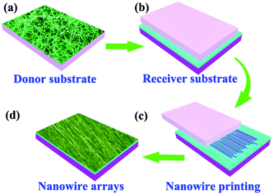 |
| | Scheme 1 Contact printing of nanowire arrays. (a) As-grown nanowire thin films on silicon substrate. (b) Covering the nanowire thin film on a receiver substrate. (c) Sliding the donor substrate from one side to another with a certain directional shear force. (d) Nanowire parallel arrays on the receiver substrate. | |
Device fabrication and measurements
Single Zn2GeO4 nanowire and In2Ge2O7 nanowire based FETs were first fabricated through a standard micro-fabrication process in a clean room in order to investigate their electrical transport properties. The as-grown nanowires were first dispersed into ethanol by sonication and then dropped onto a Si substrate with a 500 nm SiO2 insulating layer. Electrodes were then patterned on top of the nanowires using a standard optical lithography process, followed by deposition of a Ti/Al (10 nm/100 nm) film on the surface of the patterned substrate, and a lift-off process was carried out to produce the final electrode array. Multi-channel FETs were also fabricated by using the aligned Zn2GeO4 nanowire parallel arrays and the In2Ge2O7 nanowire parallel arrays as the active materials, respectively, using the same method. Briefly, following the transfer of the nanowire film onto the Si/SiO2 substrate, photolithography, deposition and lift-off processes were used to fabricate parallel Ti/Al (10 nm/100 nm) electrodes on the nanowire parallel arrays. The output (IDSvs. VDS), transfer (IDSvs. VGS) characteristics and the photoresponse performance of all the fabricated devices were measured at room temperature using a probe station connected to a Keithley 4200-SCS semiconductor characterization system. The illumination source for photoresponse measurements was a power adjustable monochromatic light source.
Results and discussion
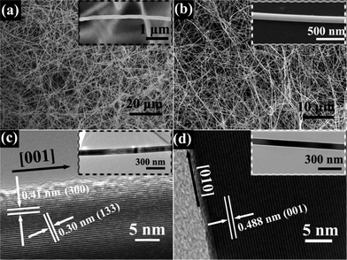
After synthesis, pure Zn2GeO4 and In2Ge2O7 nanowires were grown randomly on the silicon substrate and Fig. 1 shows the corresponding SEM and TEM results of the as-obtained products. Fig. 1(a) is a general SEM image of the as-deposited Zn2GeO4 nanowires, in the form of random nanowire mats. The length of the nanowires was measured to be about hundreds of micrometers. A magnified SEM image of a single Zn2GeO4 nanowire is shown in the inset of Fig. 1(a), where the diameter of the nanowire is calculated to be around 150 nm. Fig. 1(c) is the corresponding high resolution transmission electron microscopy (HRTEM) image of the Zn2GeO4 nanowire and the inset is a TEM image of an individual Zn2GeO4 nanowire. It is concluded that the as-synthesized Zn2GeO4 nanowires are single crystals with the growth axis along the [001] direction. Fig. 1(b) and (d) are the SEM and HRTEM images of the as-synthesized In2Ge2O7 nanowires, respectively. The insets show that the In2Ge2O7 nanowires have a size distribution with diameters of around 100–125 nm and lengths in the order of several hundred micrometers. The lattice fringe image in Fig. 1(d) indicates the single-crystalline characteristics of the nanowires with the preferred [010] growth direction.
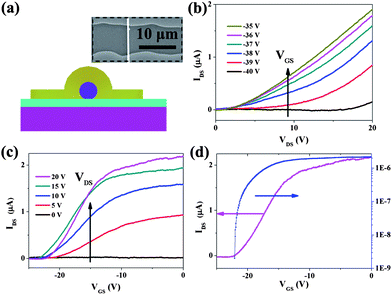
Semiconductor nanowires are often selected as the key building blocks for a variety of electronic and optoelectronic devices. A typical nanowire based nanodevice is the nanowire field-effect transistor (NW-FET). Fabricating semiconductor nanowires into FETs is an efficient way to evaluate the electronic and optoelectronic performance of the nanowires compared with their corresponding planar thin films or triaxial bulk counterparts. Fig. 2(a) shows a schematic diagram of the single nanowire based FET device on Si/SiO2, with two symmetrical Ti/Al electrodes, namely source and drain electrodes, respectively. We use the 500 nm thick SiO2 layer as the dielectric layer and the Si substrate as the gate electrode. Inset in Fig. 2(a) is the SEM image of a representative FET based on a single Zn2GeO4 nanowire. The distance between source and drain is 55.7 μm.
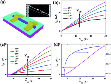 |
| | Fig. 2 (a) A schematic illustration of a single Zn2GeO4 nanowire FET. Inset is a SEM image of the device. (b) IDS–VDS curves, (c) IDS–VGS curves of a representative transistor. (d) IDS–VGS recorded for the same device plotted on linear (magenta) and logarithmic (blue) scales at VDS = 30 V. | |
The performance of the fabricated single nanowire and multi-channel FET devices was then studied in detail. Fig. 2(b–d) depict the electrical characteristics of the single Zn2GeO4 NW-FET in back-gate configuration. From the output (IDSvs. VDS) characteristics shown in Fig. 2(b), we can see that VGS shows good control of IDS and the linear curves reveal good ohmic contact between the electrodes and the nanowires. The Zn2GeO4 nanowire shows typical n-type semiconducting behaviour, as positively increasing voltages (VGS) lead to an increase in conductivity. Fig. 2(c) shows the transfer (IDSvs. VGS) characteristics of the single Zn2GeO4 NW-FET. The monotonous increase of IDSversus VGS also confirms the n-type conductivity of the Zn2GeO4 nanowire. Fig. 2(d) shows the IDS as a function of the VGS of the single Zn2GeO4 nanowire FET with VDS = 30 V in the linear and logarithmic scale, respectively. The threshold voltage and the maximum transconductance (gm) are ∼6 V and 112.8 nS, respectively. The on/off current ratio at VGS ranging from −6 V to 60 V and VDS of 30 V is about 2.51 × 10³. The field-effect mobility μ can be determined from the transconductance using eqn (1):27
| |  | (1) |
where
gm,
L, and
Ci are the transconductance (
gm = d
IDS/d
VGS), the
nanowire channel length (about 55.7 μm as shown in
Fig. 2(a)), and the capacitance of the gate dielectric, respectively. The capacitance
Ci can be calculated following
eqn (2):
28where
h is the dielectric thickness of SiO
2 (500 nm), and
r is the radius of the
nanowire (about 75 nm as confirmed by
SEM and
TEM).
ε0 and
εs are the dielectric constant of vacuum and the relative dielectric constant of gate insulator material (SiO
2 = 3.9), respectively. The effective mobility
μ is estimated to be 25.01 cm
2 V
−1 s
−1 and the electron carrier density is calculated to be 1.78 × 10
17 cm
−3 by
eqn (3):
| |  | (3) |
where
Vth is the threshold voltage.
29–33 Besides, the resistivity of the Zn
2GeO
4 nanowire can be calculated through
eqn (4):
| |  | (4) |
For a single Zn2GeO4 nanowire, the resistivity is calculated to be 0.00152 Ω m. The detailed information for the calculation is summarized in Table 1.
Table 1 A summary of the electrical properties for the single Zn2GeO4 and In2GeO7 nanowires FETs
|
|
Threshold voltage Vth (V) |
Transconductance gm (nS) |
Capacitance Ci (F) |
Mobility (cm2 V−1 s−1) |
I
on/Ioff ratio |
Carrier concentration n (cm−3) |
Resistivity (Ω m) |
| Zn2GeO4 |
6 |
112.8 |
4.66 × 10⁻¹⁵ |
25.01 |
2.51 × 10³ |
1.78 × 10¹⁷ |
0.00152 |
| In2Ge2O7 |
22 |
225 |
6.17 × 10⁻¹⁶ |
11.67 |
1.09 × 10³ |
9.38 × 10¹⁷ |
0.0149 |
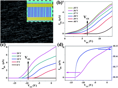
By use of the contact printing process, randomly distributed Zn2GeO4 nanowires are forced into highly ordered nanowire arrays and adhered tightly to the Si/SiO2 (500 nm) substrate. As revealed in Fig. 3(a), the Zn2GeO4 nanowires are closely assembled as parallel arrays with their longitudinal axes arranged along the sliding direction of the donor substrate. Fig. 3(b) and (c) show the output (IDSvs. VDS) and transfer (IDSvs. VGS) characteristics of the multi-channel FETs with the printed aligned Zn2GeO4 nanowire arrays as the active materials. We can see that the device shows good gate voltage modulation to the drain–source current with good saturation behavior. Compared with the single nanowire FETs, the multi-channel FETs with aligned nanowire arrays have a higher on-state current at the same gate voltage. From the linear and logarithmic plots of the IDS–VGS curves at VDS = 30 V shown in Fig. 3(d), a transconductance of 344.3 nS can be deduced. Generally speaking, the conductance of each individual Zn2GeO4 nanowire contributed equally to the multiple Zn2GeO4 nanowire FETs. So the number of nanowires actually aligned in this device is 3 and the capacitance for the multiple Zn2GeO4 nanowires FET is estimated to be 1.4 × 10⁻¹⁴ F by the sum of each individual nanowires' capacitance. Accordingly, the effective mobility is calculated to be around 25.44 cm2 V−1 s−1, which is comparable to the single Zn2GeO4 NW-FETs.
 |
| | Fig. 3 (a) SEM image of the printed aligned Zn2GeO4 nanowires arrays on the Si/SiO2 substrate. Inset is a schematic illustration of the Zn2GeO4 nanowire array based FET. (b) IDS–VDS curves and (c) IDS–VGS curves of a representative transistor. (d) IDS–VGS curves recorded for the same device plotted on linear (magenta) and logarithmic (blue) scales at VDS = 30 V. | |
Fig. 4(a) shows the side view of a back-gate FET based on individual In2Ge2O7 nanowires. The inset is the SEM image of an individual In2Ge2O7 nanowire located between the drain and source electrodes and the channel length is also measured to be about 8 μm. Representative plots of the drain–source current (IDS) versus the drain–source voltage (VDS) are shown in Fig. 4(b). With negatively increasing gate voltage (−35 V to −40 V), the conductance of the device was gradually suppressed, implying that the In2Ge2O7 nanowire also shows typical n-type semiconductor behavior. Fig. 4(c) shows plots of the drain–source current (IDS) versus the gate voltage (VGS). At the negative gate bias (VGS < 0), the source–drain currents (IDS) remain positive and monotonously increase with increased VGS, which also confirms that the single In2Ge2O7 NW-FETs exhibit n-channel depletion mode behavior. The transconductance, gm, the channel capacitance, Ci, the effective mobility, μ, and the electron concentration are then estimated to be 225 nS, 6.17 × 10⁻¹⁶ F, 11.67 cm2 V−1 s−1 and 9.38 × 1017 cm−3, respectively. The on/off current ratio at VGS ranging from −22 V to 0 V and VDS of 20 V is about 1.085 × 10³. More details about the performance of the device are summarized in Table 1.
 |
| | Fig. 4 (a) Side view illustration of a single In2Ge2O7 nanowire FET. Inset is a SEM image of the device. (b) IDS–VDS curves and (c) IDS–VGS curves of a representative transistor. (d) IDS–VGS curves recorded for the same device plotted on linear (magenta) and logarithmic (blue) scales at VDS = 20 V. | |
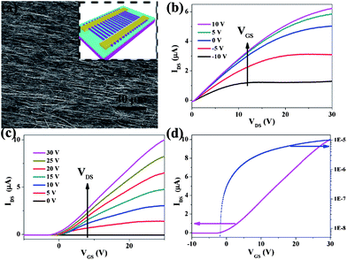
Even though the as-grown In2Ge2O7 nanowires on the donor substrate are not ordered, contact printing yielded highly oriented nanowire arrays, as shown in Fig. 5(a). The inset is the top view of a back-gate FET based on multiple nanowires. Multi-channel In2Ge2O7 NW-FETs have a higher on-state current, larger transconductance and higher voltage reliability, as shown in Fig. 5(c). These back gate structured FETs using In2Ge2O7 nanowire arrays present a threshold voltage of −13.5 V, a transconductance of 917.6 nS and a channel capacitance of 2.47 × 10⁻¹⁵ F. The effective mobility is thus determined to be 11.9 cm2 V−1 s−1 according to the transconductance calculated from the IDS–VGS curves in Fig. 5(d). The effective mobility is on a par with that of the single nanowire based FETs, indicating that contact printing did not damage the nanowires. It is believed that the superior performance of the multi-channel devices can be traced to the intrinsically high crystallinity in every single In2Ge2O7 nanowire, as well as the high degree of alignment in the nanowire arrays.
 |
| | Fig. 5 (a) SEM image of the In2Ge2O7 nanowire arrays aligned on the Si/SiO2 substrate. Inset is a schematic illustration of the In2Ge2O7 nanowire array based FET. (b) IDS–VDS curves and (c) IDS–VGS curves of a representative transistor. (d) IDS–VGS curves recorded for the same device plotted on linear (magenta) and logarithmic (blue) scales at VDS = 20 V. | |
The above results revealed that by the simple contact printing process, we are able to directly transfer and position randomly distributed Zn2GeO4 and In2Ge2O7 nanowires to form aligned nanowire arrays. Multi-channel FETs based on the printed nanowire arrays exhibited outstanding electronic performance. Such a contact printing process did not introduce any contaminants, and thus did not affect the device performance, as can be confirmed from the above discussions. Besides, the comparable device performance of the multi-channel FETs based on aligned Zn2GeO4 and In2Ge2O7 nanowire arrays indicates the advantages of the contact printing process in terms of fault tolerance.34 We suppose that the printed aligned nanowires line up in order with appropriate densities, resulting in the formation of several parallel conducting paths within the conducting channel. This means that the electron pathways will still exist, provided that some nanowires have been broken. In turn, this ensures that the performance of the multi-channel device remains almost undamaged, as can be seen from the comparable performance with single nanowire FETs.
To demonstrate the possible applications of the multi-channel FETs, we applied these FETs as high performance photodetectors. Zn2GeO4 and In2Ge2O7 nanowires have been proved to have superior response to detect ultraviolet irradiation due to their wide band gaps (4.68 eV for Zn2GeO4 and 4.43 eV for In2Ge2O7).23–26Fig. 6(a) shows typical current versus voltage (I–V) relations of the printed Zn2GeO4 nanowire array based photodetector in the dark and under illumination with ultraviolet light of different wavelengths. It is observed that the device is sensitive to ultraviolet light with both wavelengths of 254 nm and 365 nm. Shorter wavelengths surely induce higher photocurrent due to the higher energy of the photons. High photocurrents of ∼2.9 μA and ∼2.1 μA were recorded, respectively, at a bias of 10 V when the photodetector was exposed to 254 nm and 365 nm light, respectively. Fig. 6(b) shows the I–V relations of the photodetector under 254 nm light illumination with incremental intensities. Light intensity was modulated by applying a gradually increased driving voltage onto the ultraviolet light source. Clearly, the photocurrent increased with increased light intensity. Under a light intensity of 0.4 mW cm−2, the photocurrent reached 2.2 μA at 7.5 V, resulting in a photosensitivity of about 21.2 (i.e., photosensitivity = Iphoto/Idark − 1). The corresponding dependence of photocurrent on light intensity can be fitted to a power law, ΔI = APθ, where ΔI = Iphoto − Idark, P is the light intensity, A is a proportionality constant, and θ is an empirical value. Based on the experimental values, the fitting gives an exponential function with A = 4.73 and θ = 0.85. In addition, the responsivity (Rλ) of the present photodetector is calculated to be 2.11 × 10⁴ A W−1 by the relation: Rλ = ΔI/PS, where P is the light intensity irradiated on the nanowire arrays, and S is the effective illuminated area. The photoconductive gain (G, defined as the number of charges collected by electrodes due to excitation by one photon) and the quantum efficiency (QE, defined as the number of carriers circulating through a photodetector per absorbed photon and per unit time) are key parameters to evaluate the sensitivity of a photodetector. The photoconductive gain (G) and the quantum efficiency (QE) can be expressed by the following equations:25
| |  | (5) |
| |  | (6) |
where
Poptical is the light power absorbed by the effective semiconductor conductive channel,
h is Planck's constant,
hν is the energy of an incident
photon and
q is the electron charge. The photoconductive gain (
G) and the quantum efficiency (QE) of the present photodetector irradiated by 254 nm ultraviolet light at 0.4 mW cm
−2 are calculated to be 1.034 × 10
5 and 1.032 × 10
7%, respectively. These values are much higher than those of individual Zn
2GeO
4 nanowire based Schottky photodetectors (corresponding gain ∼200),
24 indicating its higher sensitivity. QE is a quantitative expression describing the process of electron–hole generation, trapping, and recombination. The lifetime of carriers (
tlife) and the transit time between electrodes (
ttran) are found to relate to the value of QE, expressed by the equation:
35–37
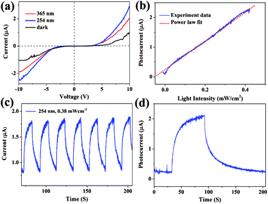 |
| | Fig. 6 (a) I–V curves of the horizontally aligned Zn2GeO4 nanowires arrays exposed to light of different wavelengths at a constant intensity of 0.38 mW cm−2. (b) The light intensity dependence of the photocurrent measured at a voltage of 7.5 V (blue line). The red dashed line shows the fitting results by the equation I = 4.73P0.85. (c) Photoresponse characteristics of the device. (d) Zoomed-in view of the middle cycle. | |
There are many factors that can largely affect tlife and ttran. First, ttran = l/ν = l/μE where l is the electrode distance, ν is the carrier drift velocity, μ is the field-effect mobility and E is the applied electric field. From our measurements, we can deduce that ttran is a very small value, which guarantees an ultrahigh quantum efficiency. Besides, the large surface-to-volume ratio of the nanowires largely increases the number of surface trap states, thus prolonging tlife. The one-dimensionality of the nanowires can confine the active area of the charge carriers and hinder the diffusion process, which result in a short ttran. Both of these two factors contribute to the ultrahigh quantum efficiency. Similar results were also found for other 1-D nanostructures.
The photoresponse switching behaviour of the horizontally aligned Zn2GeO4 nanowire array based photodetectors was measured by periodically turning on and off 254 nm light with a light intensity of 0.4 mW cm−2 at a bias of 7.5 V, as shown in Fig. 6(c) and (d). Relatively long response and relaxation times (27.6 s and 49.58 s) have been observed, which is related to the so-called persistent photoconductivity (PPC). In the photon excitation process, high-energy UV photons excite charge carriers to higher energy states and subsequently lead to a time-consuming relaxation period. It has been demonstrated that high photoconductive gain is often accompanied by a slow response time.24,25
Previously, individual In2Ge2O7 nanowire based photodetectors were demonstrated as high-performance solar-blind photodetectors.24 However, the photocurrent of the individual In2Ge2O7 nanowire based photodetectors only reached tens of nanoamperes. As we demonstrated above, a multi-channel structure exhibited a much higher photocurrent, as the active area of the device is largely increased. Here, it also applied to the multi-channel In2Ge2O7 nanowire arrays. Fig. 7(a) depicts the light intensity-dependent I–V curves of the horizontally aligned In2Ge2O7 nanowire array based photodetectors. Photocurrent rose to 3.5 μA at a bias voltage of 10 V under a 254 nm UV light illumination with an intensity of 1.6 mW cm−2. Fig. 7(b) shows the dependence of photocurrent (ΔI) on light intensity (P). Fitting the experimental data gives a relationship of ΔI = 1.91P0.85. Furthermore, the responsivity (Rλ) of the present photodetector irradiated by 254 nm light at 1.8 mW cm−2 was calculated to be 5.35 × 10⁴ A W−1. The corresponding G and QE were estimated to be 2.58 × 10⁵ and 2.617 × 10⁷%, respectively. The time-dependent photoresponse of the device was also measured and the results were shown in Fig. 7(c) and (d). Response and relaxation times were found to be around 0.86 s and 2.83 s, respectively, also indicating a trade-off between photoconductive gain and response time, similar to horizontally aligned Zn2GeO4 nanowire arrays.24,25
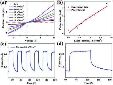 |
| | Fig. 7 (a) I–V curves of In2Ge2O7 nanowire arrays exposed to light of varied intensity. (b) The light intensity dependence of the photocurrent measured at a voltage of 7.5 V (solid squares). The solid dashed line shows the fitting results by the equation I = 1.91P0.85. (c) Photoresponse characteristics of the device. (d) Zoomed-in view of the middle cycle. | |
Conclusions
In conclusion, through the direct contact printing method, randomly distributed as-grown Zn2GeO4 and In2Ge2O7 nanowires were successfully printed into highly ordered horizontally-aligned nanowire arrays. Multi-channel FETs based on the printed nanowire arrays exhibited comparable effective mobilities with those of the single nanowire devices. Due to the multiple nanowire channels, higher transconductance, higher on-state current, and higher voltage reliability were obtained for the multi-channel FETs. The photoresponse properties of the multi-channel FETs were also studied. The Zn2GeO4 nanowire array based photodetectors exhibit excellent optoelectronic performance in terms of high responsivity (2.11 × 10⁴ A W−1), high photoconductive gain (1.034 × 10⁵) and high quantum efficiency (1.032 × 10⁷%). The In2Ge2O7 nanowire array based photodetectors also show very high responsivity (5.35 × 10⁴ A W−1), high photoconductive gain (2.58 × 10⁵) and high quantum efficiency (2.617 × 10⁷%). Our results demonstrated that the printed horizontal-aligned Zn2GeO4 and In2Ge2O7 nanowires arrays are excellent candidates for low-cost, and large-scale electronics. The continuous efforts in ternary metal oxide nanowires printing will produce promising and practicable nano-electric devices, even with the features of excellent flexibility and portability.
Acknowledgements
This work was supported by the National Natural Science Foundation (91123008, 51002059, 21001046), the 973 Program of China (2011CBA00703, 2011CB933300), the Program for New Century Excellent Talents of the University in China (grant no. NCET-11-0179), the Research Fund for the Doctoral Program of Higher Education (20100142120053) and the Natural Science Foundation of Hubei Province (2011CDB035). Special thanks to the Analytical and Testing Center of HUST and the Center of Micro-Fabrication and Characterization (CMFC) of WNLO for using their facilities.
Notes and references
- W. I. Park, J. S. Kim, G. C. Yi and H. J. Lee, Adv. Mater., 2005, 17, 1393 CrossRef CAS.
- J. Huang and Q. Wan, Sensors, 2009, 9, 9903 CrossRef.
- Z. Wang, S. Ran, B. Liu, G. Z. Shen and D. Chen, Nanoscale, 2012, 4, 3350 RSC.
- K. W. Liu, M. Sakurai and M. Aono, Sensors, 2010, 10, 8604 CrossRef CAS.
- D. Chen, Z. Liu, B. Liang, X. F. Wang and G. Z. Shen, Nanoscale, 2012, 4, 3001 RSC.
- J. M. Bao, M. A. Zimmler and F. Capasso, Nano Lett., 2006, 6, 1719 CrossRef CAS.
- M. Law, L. E. Greene, J. C. Johnson, R. Saykally and P. D. Yang, Nat. Mater., 2005, 4, 455 CrossRef CAS.
- Z. Y. Fan, J. C. Ho, Z. A. Jacobson, H. Razavi and A. Javey, Proc. Natl. Acad. Sci. U. S. A., 2008, 105, 11066 CrossRef CAS.
- B. Y. Lee, M. G. Sung, H. Lee, S. Namgung, S. Y. Park, D. S. Choi and S. Hong, NPG Asia Mater., 2010, 2, 103 CrossRef.
- A. C. Ford, J. C. Ho, Z. Y. Fan, O. Ergen, V. Altoe, S. Aloni, H. Razavi and A. Javey, Nano Res., 2008, 1, 32 CrossRef CAS.
- Y. Huang, X. F. Duan, Q. Q. Wei and C. M. Lieber, Science, 2001, 291, 630 CrossRef CAS.
- D. Whang, S. Jin and C. M. Lieber, Jpn. J. Appl. Phys., 2004, 43, 4465 CrossRef CAS.
- D. Whang, S. Jin, Y. Wu and C. M. Lieber, Nano Lett., 2003, 3, 1255 CrossRef CAS.
- Y. Z. Long, M. Yu, B. Sun, C. Z. Gu and Z. Y. Fan, Chem. Soc. Rev., 2012, 41, 4560 RSC.
- D. H. Kim, N. S. Lu, R. Ghaffari and J. A. Rogers, NPG Asia Mater., 2010, 4, 1 Search PubMed.
- A. Javey, S. Nam, R. S. Frienman, H. Yan and C. M. Lieber, Nano Lett., 2007, 7, 773 CrossRef CAS.
- T. Takahashi, K. Takei, J. C. Ho, Y. L. Chueh, Z. Y. Fan and A. Javey, J. Am. Chem. Soc., 2009, 131, 2102 CrossRef CAS.
- Z. Y. Fan, J. C. Ho, Z. A. Jacobson, R. Yerushalmi, R. L. Alley, H. Razavi and A. Javey, Nano Lett., 2008, 8, 20 CrossRef CAS.
- Z. Y. Fan, J. C. Ho, T. Takahashi, R. Yerushalmi, K. Takei, A. C. Ford, Y. L. Chueh and A. Javey, Adv. Mater., 2009, 21, 3730 CrossRef CAS.
- D. Chen, J. Xu, B. Liang, X. F. Wang, P. C. Chen, C. W. Zhou and G. Z. Shen, J. Mater. Chem., 2011, 21, 17236 RSC.
- H. T. Huang, B. Liang, Z. Liu, X. F. Wang, D. Chen and G. Z. Shen, J. Mater. Chem., 2012, 22, 13428 RSC.
- B. Liu, J. Zhang, X. Wang, G. Chen, D. Chen, C. W. Zhou and G. Z. Shen, Nano Lett., 2012, 12, 3005 CrossRef CAS.
- C. Y. Yan and P. S. Lee, Sci. Adv. Mater., 2012, 4, 241 CrossRef CAS.
- C. Li, Y. Bando, M. Y. Liao, Y. Koide and D. Golberg, Appl. Phys. Lett., 2010, 97, 161102 CrossRef.
- L. Li, P. S. Lee, C. Y. Yan, T. Y. Zhai, X. S. Fang, M. Y. Liao, Y. S. Koide, Y. Bando and D. Golberg, Adv. Mater., 2010, 22, 2145 Search PubMed.
- Z. Liu, H. T. Huang, B. Liang, X. F. Wang, Z. R. Wang, D. Chen and G. Z. Shen, Opt. Express, 2012, 10, 2982 CrossRef.
- G. Z. Shen, J. Xu, X. F. Wang, H. T. Huang and D. Chen, Adv. Mater., 2011, 23, 771 CrossRef CAS.
- G. Z. Shen, B. Liang, X. F. Wang, P. C. Chen and C. W. Zhou, ACS Nano, 2011, 5, 2155 CrossRef CAS.
- D. suh, S. Y. Lee, J. H. Hyung, T. H. Kim and S. K. Lee, J. Phys. Chem. C, 2008, 112, 1276 CAS.
- G. Z. Shen, J. Xu, X. F. Wang, H. T. Huang and D. Chen, Adv. Mater., 2011, 23, 771 CrossRef CAS.
- K. Kim, P. C. Debnath, S. Kim and S. Y. Lee, Appl. Phys. Lett., 2011, 98, 113109 CrossRef.
- Y. W. Heo, L. C. Tien, Y. Kwon, D. P. Norton and S. J. Pearton, Appl. Phys. Lett., 2004, 85, 22749 Search PubMed.
- D. Wu, J. Yang, Y. G. Zhang, J. W. Li, Y. Q. Yu, Y. P. Zhang, Z. F. Zhu, L. Wang, C. Y. Wu, L. B. Luo and J. S. Jie, J. Mater. Chem., 2012, 22, 6206 RSC.
- Z. B. He, W. J. Zhang, W. F. Zhang, J. S. Jie, L. B. Luo, G. D. Yuan, J. X. Wang, C. M. L. Wu, I. Bllo, C. S. Lee and S. T. Lee, J. Phys. Chem. C, 2010, 114, 4663 CAS.
- G. Beadie, W. S. Rabinovich, A. E. Wickenden, D. D. Koleske, S. C. Binari and J. A. Freitas, Appl. Phys. Lett., 1997, 71, 1092 CrossRef CAS.
- L. Li, P. C. Wu, X. Fang, T. Y. Zhai, L. Dai, M. Y. Liao, Y. S. Koide, H. Q. Wang, Y. Bando and D. Golberg, Adv. Mater., 2010, 22, 3161 CrossRef CAS.
- W. Tian, C. Y. Zhi, T. Y. Zhai, X. Wang, M. Y. Liao, S. L. Li, S. M. Chen, Y. Bando and D. Golberg, Nanoscale, 2012, 4, 6318 RSC.
|
| This journal is © The Royal Society of Chemistry 2013 |
Click here to see how this site uses Cookies. View our privacy policy here.