 Open Access Article
 This Open Access Article is licensed under a Creative Commons Attribution-Non Commercial 3.0 Unported Licence
Alignment of helical nanofilaments on the surfaces of various self-assembled monolayers†
Hanim
Kim
a,
Sunhee
Lee
a,
Tae Joo
Shin
b,
Yun Jeong
Cha
a,
Eva
Korblova
c,
David M.
Walba
c,
Noel A.
Clark
d,
Sang Bok
Lee
ae and
Dong Ki
Yoon
*a
aGraduate School of Nanoscience and Technology (WCU) and KINC, KAIST, Daejeon 305-701, Republic of Korea. E-mail: nandk@kaist.ac.kr; Fax: +82 42 350 1110; Tel: +82 42 350 1116
bPohang Accelerator Laboratory, POSTECH, Pohang, 790-784, Rep. of Korea
cDepartment of Chemistry and Liquid Crystal Materials Research Center, University of Colorado, Boulder, CO 80309, USA
dDepartment of Physics and Liquid Crystal Materials Research Center, University of Colorado, Boulder, CO 80309, USA
eDepartment of Chemistry and Biochemistry, University of Maryland, College Park, MD 20742, USA
First published on 4th June 2013
Abstract
We successfully prepared controlled layers of NOBOW molecules on a variety of self-assembled monolayers (SAMs) such that the layers formed oriented domain structures in which the complex chiral/polar crystalline helical nanofilaments (HNFs) were arranged to form a B4 bent-core liquid crystal (LC) phase. The alignment of the B2 phase, which formed at a higher temperature than the B4 phase, affected the direction of the HNFs. The HNFs formed on the B2 smectic layers and were aligned parallel or perpendicular, respectively, to the substrates with high or low surface energies (molecule-philic or -phobic SAM-treated substrates). The HNFs confined within rectangular microchannels modified by the SAMs were directly visualized by electron microscopy and X-ray diffraction studies. The orientations of the HNFs were found to be governed by the B2 smectic layer morphology.
1 Introduction
Bent-core liquid crystal (LC) phases composed of achiral molecules display unusual collective behaviours that result in the formation of chiral superstructures in “banana” or B phases.1–7 A detailed understanding of each B phase has been difficult to obtain4,5,7 due to the structural complexities of the macroscopic domains. Such domains are required for the preparation of second-order nonlinear optical materials, optical displays, and electro-optic responsible devices.8–10 Many smectic phases do not pass through an intervening nematic phase upon cooling from an isotropic phase; therefore, large oriented B phase domains are not easily prepared using conventional surface treatment methods that are generally effective for the alignment of conventional LCs.11–13 Although topographic patterning can successfully align the B phases,14,15 these methods are not easily applied to large domains.Among the B phases that are difficult to control, it is very difficult to obtain large single domains of helical nanofilaments (HNFs) in the B4 phase. The morphologies of these phases are driven by a local saddle splay deformation between the polar and chiral B2 smectic LC layers. The specific handedness and bouquet-like growth of nano-segregated domains are prevented in the formation of large domains (Fig. 1b and c).7 HNFs grown from a higher-temperature isotropic bent-core molecule–nematic mixture phase16 or a fluid bent-core phase (e.g., B2)7 have a well-defined width (w) (∼35 nm) and half pitch (h) (∼110 nm) (Fig. 1c). Such domains have been directly visualized using freeze-fracture TEM and atomic force microscopy (AFM) studies.7 NOBOW molecules (Fig. 1a) form B2/B3 phases in a smectic layer morphology prior to transitioning to a B4 phase upon cooling. The chevron texture induced by the tilted molecules in a smectic C phase, here a B2 (SmCP) phase, may potentially form on planar molecule-philic substrates (Fig. 1d).17 The perpendicular alignment of bent-core molecules in B2 layers may be obtained on molecule-phobic surfaces (Fig. 1e). These arrangements of NOBOW molecules and smectic layers can govern the orientations of HNFs after transiting to a B4 phase (Fig. 1f and g).
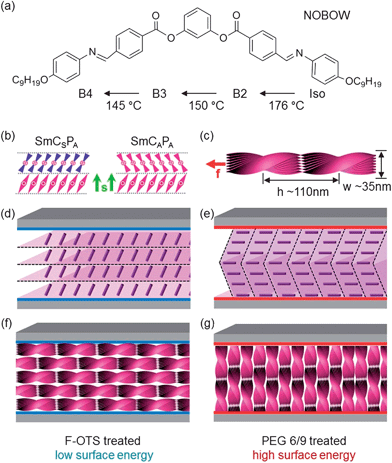 | ||
| Fig. 1 Bent-core molecule, molecular organization of B2/B4 phases and their alignment on molecule-philic/phobic substrates. (a) The chemical structure and phase transition on cooling of NOBOW molecules. (b) Smectic layers can be found at the B2 phase, and s is a layer normal vector. (c) The formation of helical nanofilaments (HNFs) at the B4 phase. The width (w) and half pitch (h) of a single filament is ∼35 nm and ∼110 nm respectively. f is the long axis of HNFs. Schematic sketches of two possible alignments of the B2 smectic phase between molecule-phobic substrates (d) and molecule-philic substrates (e). Typical chevron structure can be found in the planar aligned B2 phase. (f and g) The followed arrangements of HNFs in F-OTS and PEG6/9 treated cells. | ||
Here, we describe a method for controlling the orientation of B4 HNFs by chemically modifying solid substrates using self-assembled monolayers (SAMs) having a variety of chemical groups. Methods of grafting small molecules chemisorbed onto solid substrates are generally simple, reproducible, and create well-ordered functionalities and good chemical and thermal stability under ambient conditions.18–20 Depolarized reflection light microscopy (DRLM) and scanning electron microscopy (SEM) techniques were used to characterize the controlled HNFs and the B2 smectic layers prepared on the modified solid substrates. Grazing incidence X-ray diffraction (GIXD) methods were used to confirm the B2/B4 layering orientations as a function of the surface energy induced by each SAM. The surface energy induced thermal phase transitions in the B4 and B2 phases during cooling from an isotropic state were also characterized.
2 Results and discussion
The relative surface energies of the NOBOW layers prepared on each chemically modified substrate or bare silicon wafer were determined based on contact angle (CA) measurements from a melted NOBOW droplet at 190 °C (Fig. 2c). The surface energy value at the B2/B4 phase transition was difficult to determine with precision; however, the relative properties of the surfaces could be estimated. An LC droplet on a semi-fluorinated tri-decafluoro-1,1,2,2-tetrahydrooctyl-trichororosilane (F-OTS) SAM (Fig. 2a) showed the highest CA (the lowest surface energy), whereas the CA on a PEG6/9 (2-(methoxy(polyethylenoxy)-propyl)trimethoxysilane) surface (Fig. 2b), which presented relatively “molecule-philic” functionalities displayed a low CA. This surface yielded the highest surface energy among the three surfaces examined here.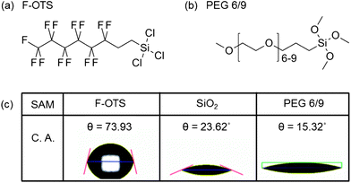 | ||
| Fig. 2 Self-assembled monolayers (SAMs) and their contact angle (CA) measurements. (a and b) The two self-assembled monolayer-forming molecules used in this study: molecule-philic (a) and molecule-phobic (b). (c) CAs of the NOBOW molecule layers prepared on each SAM at 190 °C, indicating that different surface energies resulted from the layers prepared on the different surfaces. | ||
The bent-core NOBOW molecules transitioned to a B2 phase during cooling from a higher-temperature isotropic phase prepared in a gap a few microns thick between a silicon wafer and a glass plate. The surfaces of the silicon wafer and glass plate had been functionalized by SAMs. During the thermal transition, distinct stripes running parallel to the smectic layers were observed over the majority of the sample, examples of which are shown in Fig. 3a and c. The images were recorded under isothermal conditions upon cooling from an isotropic region to a B2 phase at a rate of 5 °C min−1 (ESI, Fig. S1†). The optical textures observed on the F-OTS and SiO2 substrates were compared. Only a few nucleation points were observed on the SiO2 surface (Fig. 3a), then these domains grew and eventually coalesced into larger aggregates. By contrast, relatively many nucleation points formed very small clusters on the F-OTS surface (Fig. 3c). The NOBOW molecules formed specific surface–anchoring interactions with the differently treated substrates, and show self-stabilizing intermolecular interactions to form the preferred layering structures. These interactions competed for dominance during the iso-to-B2 transition. Differences in the substrate anchoring strengths on the various surfaces led to different anisotropic optical textures in the resulting B2 phases. For this reason, striped patterns resulted from the alternating tilt directions of the synclinic antiferroelectric polar smectic C (SmCSPA) phase in the layered structures.4 These structures were not prominent in the sample prepared on the F-rich functionalized surface under low magnification (ESI, Fig. S2†). This trend was observed within the relatively bright domains of the blue-coloured domains on the SiO2 surfaces in the B4 phases (ESI, Fig. S1†). Birefringence in the B4 phase was quite small due to averaging of the molecular orientations in the HNFs (Fig. 3b, d and f).7
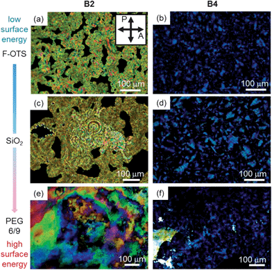 | ||
| Fig. 3 Polarization optical imaging reveals the textures of the surface layers during the phase transition from the B2 to the B4 phase on each substrate (a, c and e). The DRLM images highlight bright optical anisotropy of the B2 smectic layers, (b, d and f) whereas the mostly dark and bluish-to-yellowish coloured domains correspond to B4 phases that formed on all substrates. Under the PEG6/9 grafting conditions, an oil-on-water morphology was observed in the B2 phase, and crystal-like defects remained even after a long period of time (several hours). The left-hand legends and arrows indicate the relative surface energies of the SAMs. | ||
A DRLM image of the B2 phase on a PEG6/9 SAM revealed morphologies that were very different from those observed on the F-OTS and SiO2 surfaces. Oil-on-water-interference colours were observed over large areas (Fig. 3e), even though the B4 textures did not differ significantly from the textures of the other samples. These results indicated that the molecular arrangements in the B2 layers prepared between the PEG6/9-modified surfaces differed from the textures of the other samples. The observed birefringent colour was quite unusual for the B2 phase and originated from the close packing of the planar bent-core molecules in PEG6/9 treated cells. This structure yielded a certain value of Δn, as shown in the Michel–Lévy interference colour chart.21 The striped patterns or a simple smectic A-like morphology which is typical of the B2 phase (Fig. 3a and c) did not appear.4 Instead, long-range ordered morphologies resulting from the strong surface anchoring effects of the PEG6/9-NOBOW surface are found.
These unique optical structures observed in DRLM were directly imaged using electron microscopy techniques. The layering structures were prepared by quenching B2 phase samples by rapidly immersing them into liquid nitrogen to trap the B2 structure. The samples were then warmed back to room temperature. Deep-freezing the NOBOW sample in the B2 phase was the only way to capture this structure because under slow cooling, transitions to other phases, such as the B4 crystalline phase, occurred. Investigations of the HNFs and B4 phases did not require a deep-freeze method; instead, the samples were cooled all the way to room temperature from the isotropic phase. SEM analysis of the cross-sectioned samples was conducted to characterize the internal alignment of the smectic layers. One of the SAM treated substrates in the cell was removed and a sub 3 nm thick layer of platinum was sputter-coated to facilitate visualization of the surface topography.
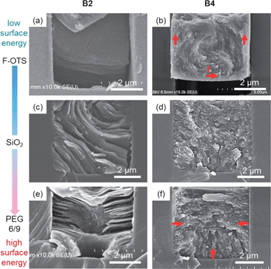
The cross-sectional SEM views of the B2 phase, typical examples of which are shown in Fig. 4, revealed many layer structures on the micron-scale. The various samples yielded parallel alignment (F-OTS), normal alignment (PEG6/9), or random alignment (SiO2) of the layers on the substrates, as shown in the layer-normal vectors (green arrows) (Fig. 4a, c and e). The NOBOW molecules were shown to form layers with homeotropic (F-OTS) or planar (PEG6/9) alignment, consistent with the DRLM imaging results (Fig. 3).
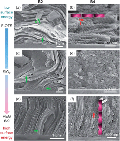 | ||
| Fig. 4 Direct visualization of the various aligned B2 layers and guided HNF layers formed between the chemically modified substrates. (a, c and e) The cross-sectional views shown in the SEM images revealed the alignment of the B2 smectic layers, in which s was mostly perpendicular (a), or parallel (e) to the substrates. s was evenly distributed on the SiO2 surface (c), indicating that the surface energy of the SAM could control the orientations of the B2 smectic layers. (b, d and f) The HNF alignment guided by the B2 phase corresponded to the director f on the different substrates. | ||
Although most of the layers were parallel to the F-OTS-treated substrate, some of the layers formed a 1/2 disclination in the middle of the sample due to the elastic contribution of the B2 smectic phase (ESI, red circle in Fig. S2†). This small region formed tiny anisotropic optical domains that formed an alternative arrangement of the SmCSPA layers due to different nucleation properties. Oriented domains with a layered structure were observed near the F-OTS-treated surfaces and formed small regions of randomly oriented layers in the middle of the film, as shown in Fig. 4a (green arrow). The bright optical signals of these B2 smectic layers with homeotropic alignment displayed biaxial optical properties and disclination-like morphologies (Fig. 3a).
The B2 layers that formed between the SiO2 substrates were mostly random, i.e., a mixture of parallel, perpendicular, and tilted orientations relative to the substrate, as shown in the cross-sectional SEM image (Fig. 4c). The focal conic domains that are usually found in smectic phases were also observed, indicating that the surface conveyed relatively weak planar orientations among the B2 layers. The orientations of the B2 layers dramatically improved on the PEG6/9 surface, which displayed the highest surface energy. The magnified view near the substrate (Fig. 4e) revealed that all of the layers were aligned perpendicular to the surface. Certain warped layers formed chevron-like structures in the smectic samples grown in thin gaps between the flat plates. These layers underwent layer shrinkage (Fig. S3 in ESI†), for example, during the SmA to SmC phase transition.17 The strong anchoring properties of the PEG6/9 functional groups and the NOBOW molecules affected B2 layer formation and created a large domain without stipe-like domains, as shown in the DRLM image (Fig. 3e).
These trends were more easily observed in the SEM images of the B4 phase, in which the direction of each HNF was determined by the B2 layer structure. For example, many of the HNF layers on the F-OTS-treated substrate displayed planar alignment with a clearly discernible polarization director,  , as shown in the model sketch presented in Fig. 1c, f and 4b. Interestingly, the director vector, s, which was determined for the B2 phase, was related to the orientation of the B4 phase. This relationship offered a method for guiding the alignment of the complex HNFs over large areas. This trend was also observed in the SiO2 and PEG6/9 samples (Fig. 4d and f). The HNFs formed between the SiO2 substrates were randomly oriented, as expected based on the SEM images of the B2 phase; however, the HNF layers formed on the PEG6/9-treated surface mainly displayed a perpendicular arrangement of molecules over a large area, as illustrated in Fig. 1g. It is difficult to say whether the layer normal director of the B2 smectic phase, s, was perpendicular or parallel to the substrates in the B4 phase because the HNFs are intrinsically twisted, and s gradually changed through the direction. Considering that the HNFs acted as simple discrete ropes, most of the layer normal vectors in the HNF layers were coincident with the B2 layer normal vector, s. This coincidence may potentially explain the correlated behaviours of the B2 and B4 phases.
This relationship was further examined by varying the boundary conditions to test silicon microchannels with different widths (3, 5, 7, 10 μm, etc.) and a fixed depth (5 μm) and length (10 mm). The 5 μm channel displayed typical properties (Fig. 5). Rectangular microchannel grooves were prepared on the surfaces of single crystal Si substrates ((100) orientation) using conventional photolithographic masking techniques, followed by reactive ion etching with CF4.22 The surfaces were then functionalized with SAMs to promote control over the orientations of the B phases, as performed in the DRLM and bulk SEM experiments. Each channel was filled with NOBOW molecules by heating the substrate surface (open to air) to a temperature in the isotropic range of the LC. A drop of the LC was then placed on one end of the channel array, and capillarity forces drew the LC into the grooves. Each sample was then cooled at a rate of 5 °C min−1 to form the B2 LC phase in the channels. The textures of the layers were then characterized by SEM after preparing cross-sectional samples after rapid freezing.
 | ||
| Fig. 5 Cross-sectional SEM images of the confined B2 and B4 phases in the 5 μm wide rectangular channels. (a, c and e) The SEM images show the topographical patterns of the B2 smectic layers. (a) All boundary conditions, including the air, bottom substrate, and two sidewalls, induced homeotropic alignment of the bent-core molecules, leading to very unstable layering structures. (b and c) Parallel alignment of the molecules on the high-energy surfaces produced focal conic domains that are typical of smectic phases.14,23 (b, d and f) The HNF growth direction was determined by the B2 smectic layers on the substrates. | ||
In a previous study, the smectic layers formed on clean silicon microchannels were found to be bent at the center of the toric focal conic domains (TFCDs) due to antagonism between the surface anchoring conditions: tangential alignment was promoted by the bottom surface, and vertical alignment was promoted near the air boundary. The cross-sectional view shown in Fig. 5e revealed the same structure. The smectic layers were oriented normal to the side walls and were curved toward the bottom plate, at which point they formed concentric circles, as expected for TFCDs.23 The formation of TFCDs in a channel results from the establishment of balance between the surface anchoring forces and the elastic energies.24 As shown in the cross-sectional view, the molecules preferred to be oriented parallel to the walls and perpendicular to the free surfaces of the smectic films. These boundary conditions could be satisfied only when the layers were bent, preferably with a minimum elastic energy cost. The latter was achieved by constructing a TFCD, in which the defects were two singular lines: a circular line at the bottom and a vertical straight line.25 The layer morphology was observed to deviate from the ideal TFCD geometry, possibly due to the roughness of the walls (Fig. 5e).
The surface anchoring properties were controlled by introducing surface modifications. The SiO2 surface formed weaker surface anchoring interactions than the PEG6/9 surface, whereas the F-OTS surface formed much weaker interactions between the functional groups on the substrates and the NOBOW molecules. The F-OTS experiments mainly revealed B2 smectic layers and B4 HNFs detached from the microchannel during the fracturing of the sample due to the weak adhesion forces. The surface anchoring was not sufficiently strong to hold the LC molecules onto the substrate. The layer direction was highly random, as shown in Fig. 5a, resulting in chaotic B2 layering structures and HNF arrangements in the channel (Fig. 5a and b). On the SiO2 surface, the layers were less ordered than the layers formed on the PEG6/9 surface; however, long-range ordered B2 smectic layers and HNFs were observed, as shown in Fig. 5c and d. The microchannel experimental results suggested the importance of surface anchoring properties on the formation of B2/B4 HNFs on a substrate. The B2 and B4 phases were found to be closely related during the thermal phase transition.
To confirm that the SAM could be used to control the orientations of the B2/B4 phases, GIXD experiments using a synchrotron radiation source were carried out. As in the SEM experiments, all samples used in the XRD experiments were quenched in the B2 phase. Following the first heating and second cooling of the sample, the oriented diffraction patterns disappeared and arc patterns appeared, indicating a loss of orientation. The peak positions of the samples differed slightly from the peak positions in the bulk B2 phase due to shrinkage of the smectic layers during the quenching procedure. The B2 and B4 phases appeared to coexist in the quenched samples examined by GIXD. Relatively sharp peaks were observed at wide angles, as shown in Fig. 6c, indicating the crystal-like packing of the NOBOW molecules. If only the B4 phase were present the center peak in the two-dimensional (2D) diffraction patterns would not have been present because the small-angle peaks of the B4 phase displayed diagonal split diffraction patterns resulting from the helically arranged smectic layers.7 The GIXD patterns indicated that a large number of B2 layered structures were present. The X-ray beam 600 μm in diameter was large relative to the microchannel width. Despite the difference in length scales, different orientations of the B2 phases were observed in the F-OTS and PEG6/9 samples. The GIXD pattern revealed the typical internal structures and orientations of the B2 smectic layers. Fig. 6c shows the 2D GIXD pattern for the PEG6/9 sample, which revealed out-of plane layer structures. The B2 smectic layers were mainly aligned parallel to the air and bottom substrate surfaces of the confining microchannel, whereas the F-OTS sample displayed relatively random orientations of the molecules. The arc shape of the 2D GIXD pattern indicated the presence of randomly oriented nano-domains. This structure was confirmed by a 1D graph plotted along the vertical (solid line) line cut in the 2D pattern. The normalized intensities were very high in the PEG6/9 sample (Fig. 6d), whereas the horizontal (dashed line) line cut showed no features above the noise level. Most of the B2 smectic layers appeared to be aligned parallel to the substrate. As expected from the SEM images, which directly visualized the surface morphologies, randomly oriented B2 smectic layers formed on the F-OTS sample, and this layer did not display a strong intensity in Fig. 6d. The intensity along the horizontal (dashed line) line cut (Fig. 6e), however, featured only weak signals due to the random orientations of the B2 phase on the F-OTS treated substrate. The 2D GIXD patterns of the B4 phase did not show any notable features because the HNF molecules formed helical layered structures such that either the in-plane or out-of plane intensities were the same, regardless of the orientations of the HFN molecules in the microchannels (not shown here).
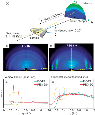 | ||
| Fig. 6 Grazing incidence X-ray diffraction (GIXD) set-up for the microchannel experiments. (a) Schematic diagram showing the GIXD configuration. The incident direction of the X-ray beam was parallel to the longitudinal axis of the microchannels. (b and c) GIXRD patterns of the microchannels are shown, in which the F-OTS and Peg6/9 results displayed distinct two-dimensional (2D) diffraction patterns. (d and e) The intensity at small angles in the vertical or horizontal line-cut graphs clearly revealed the conformations of the B2/B4 layers having distinct ordering behaviours. | ||
The orientations of the HNFs on each functionalized confined microchannel are illustrated schematically in Fig. 7. The controlled B2 phase prepared on either a molecule-philic or a molecule-phobic surface governed the directions in which the HNF molecules were aligned, which was very helpful for preparing a globally oriented single domain comprising complex HNFs.
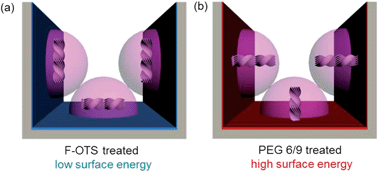 | ||
| Fig. 7 Schematic diagrams of the internal B4 phase formed in the confined geometries. (a) Circularly or randomly oriented HNFs were found on the molecule-phobic substrate, which had a low surface energy. (b) A homeotropic alignment of HNFs was prepared on the molecule-philic surface with a high surface energy. | ||
The formation of the B4 phase was sensitive to the surface functionalization chemistry. Surface anchoring interactions could adjust the phase transition to a small degree, as shown in Fig. S1.† The series of DRLM images of samples cooled from an isotropic temperature to room temperature revealed dark and bluish B4 textures at 145 °C, 143 °C, and 141 °C on the F-OTS, SiO2, and PEG6/9 surfaces, respectively. The B2/B3-to-B4 transition temperature was measured to be 145 °C in the bulk state by differential scanning calorimetry (DSC, Fig. 1a). These results could be explained in terms of the stronger surface anchoring interactions, which suppressed the saddle-splay distortion geometry of the B4-phase HNFs. The surface anchoring interactions affected the formation of lower-temperature phases and altered the alignment of the molecules on the chemically modified substrate.
3 Conclusion
In summary, we showed that the surface anchoring interaction strength could be used to control the orientations of the B2 smectic layers and the B4 HNFs. These results suggest that a variety of SAM materials may be used to control complex HNFs over large areas. Surface anchoring effects governed the initial stages of the B2 layer growth by restricting growth within a few microns of the film during the thermal phase transition. The achievement of an aligned B4 phase, which is notoriously difficult to orient using other methods, showed that the use of a variety of surface functional groups to control the molecular orientations may prove to be a powerful tool for the preparation of LC layers for use in applications that require hydrophobic surfaces, which are often difficult to align.264 Experimental
Sample preparation
The silicon wafer surface was modified using commercially available silane reagents (Gelest, Morrisville, PA). The surface was then treated with oxygen plasma. The cleaned silicon wafer and 0.5 mL as-received F-OTS (tridecafluoro-1,1,2,2-tetrahydrooctyltrichloro-silane) were placed in a cleaned and dried vial inside a desiccator under vacuum for 1 h to obtain a LC molecule-phobic surface. To prepare the LC molecule-philic surface, the silicon wafer was washed with ethanol to remove residual dust and soaked in a glass dish filled with 5% PEG6/9 (90%, 2-methoxypolyethylenoxypropyltrimethoxysilane) in a 95% ethanol–water solution. The sealed glass dish was rocked and shaken for 1 h at room temperature. Finally, the silicon wafer was washed with ethanol, dried under nitrogen, and cured at 120 °C for 1 h. A simple surface modification method using silane reagents was used as reported previously.18 The relative surface energies of the samples prepared with differently modified substrates were measured using contact angle measurement at the isotropic temperature (190 °C) (Phoenix 300 Touch, SEO). The F-OTS and PEG6/9 samples were loaded at the isotropic liquid phase (190 °C) via the capillary forces between two chemically modified substrates (a cover glass and a silicon wafer, each treated in the same manner). The spacing between the substrates was a few micrometers. The samples were then cooled to room temperature (LTS350, Linkam, UK).Characterization
The optical anisotropic textures of the LC NOBOW phases in each cell were directly visualized between crossed-polarizers using DRLM during all thermal transitions. The micro-morphological features of the B2 and B4 phases in each cell were observed using SEM (HITACHI). All samples were cross-sectioned to expose the internal structures after removing one of the substrates. The B2 layers were observed in certain samples. Some samples were analyzed after sudden quenching at 170 °C in liquid nitrogen. The microchannel experiments were conducted using the patterned substrates prepared by photolithography and reactive ion etching to have a width of 5 μm, a depth of 5 μm, and a length of 10 mm.The GIXD experiments were carried out at the 9A beamline in the Pohang Accelerator Laboratory (PAL). The size of the focused beam was 600 μm in diameter and the energy of the beam was 11 keV. The sample-to-detector distance was 220 mm, and the data were typically collected for 0.5 s at a small angle and for 1 s at a wide angle, using a two-dimensional charge-coupled device (2D CCD) detector (Rayonix SX165).
Acknowledgements
This was supported by the National Research Foundation (NRF) Grant funded by the Korean Government (MSIP & MOE) (2012R1A1A1002486, 2012R1A2A2A06046931, 2012M3A7B4049802, and R31-10071), and the MRSEC Program funded by NSF DMR-0820579. Experiments at the PLS were supported in part by MSIP and POSTECH.Notes and references
- T. Niori, T. Sekine, J. Watanabe, T. Furukawa and H. Takezoe, J. Mater. Chem., 1996, 6, 1231–1233 RSC.
- G. Pelzl, S. Diele and W. Weissflog, Adv. Mater., 1999, 11, 707–724 CrossRef CAS.
- R. A. Reddy and C. Tschierske, J. Mater. Chem., 2006, 16, 907–961 RSC.
- D. R. Link, G. Natale, R.-F. Shao, J. E. Maclennan, N. A. Clark, E. Korblova and D. M. Walba, Science, 1997, 278, 1924–1927 CrossRef CAS.
- D. A. Coleman, J. Fernsler, N. Chattham, M. Nakata, Y. Takanishi, E. Korblova, D. R. Link, R.-F. Shao, W. G. Jang, J. E. Maclennan, O. Mondainn-Monval, C. Boyer, W. Weissflog, G. Pelzl, L.-C. Chien, J. Zasadzinski, J. Watanabe, D. M. Walba, H. Takezoe and N. A. Clark, Science, 2003, 301, 1204–1211 CrossRef CAS.
- L. E. Hough, M. Spannuth, M. Nakata, D. A. Coleman, C. D. Jones, G. Dantlgraber, C. Tschierske, J. Watanabe, E. Korblova, D. M. Walba, J. E. Maclennan, M. A. Glaser and N. A. Clark, Science, 2009, 325, 452–456 CrossRef CAS.
- L. E. Hough, H. T. Jung, D. Krüerke, M. S. Heberling, M. Nakata, C. D. Jones, D. Chen, D. R. Link, J. Zasadzinski, G. Heppke, J. P. Rabe, W. Stocker, E. Körblova, D. M. Walba, M. A. Glaser and N. A. Clark, Science, 2009, 325, 456–460 CrossRef CAS.
- I. C. Pintre, J. L. Serrano, M. B. Ros, J. Martínez-Perdiguero, I. Alonso, J. Ortega, C. L. Folcia, J. Etxebarria, R. Alicante and B. Villacampa, J. Mater. Chem., 2010, 20, 2965–2971 RSC.
- T. Otani, F. Araoka, K. Ishikawa and H. Takezoe, J. Am. Chem. Soc., 2009, 131, 12368–12372 CrossRef CAS.
- A. Jákli, Liq. Cryst. Today, 2002, 11, 1–5 CrossRef.
- P. G. de Gennes and J. Prost, The Physics of Liquid Crystals, Clarendon, Oxford, 1993 Search PubMed.
- A. Rastegar, G. Wulterkens, H. Verscharen, T. Rasing and G. Heppke, Rev. Sci. Instrum., 2000, 71, 4492 CrossRef CAS.
- K. Shiromo, D. A. Sahade, T. Oda, T. Nihira, Y. Takanishi, K. Ishikawa and H. Takezoe, Angew. Chem., Int. Ed., 2005, 44, 1948–1951 CrossRef CAS.
- D. K. Yoon, R. Deb, D. Chen, E. Körblova, R.-F. Shao, K. Ishikawa, N. V. S. Rao, D. M. Walba, I. I. Smalyukh and N. A. Clark, Proc. Natl. Acad. Sci. U. S. A., 2010, 107, 21311–21315 CrossRef CAS.
- D. K. Yoon, Y. Yi, Y. Shen, E. Korblova, D. M. Walba, I. I. Smalyukh and N. A. Clark, Adv. Mater., 2011, 23, 1962–1967 CrossRef CAS.
- D. Chen, C. Zhu, R. K. Shoemaker, E. Korblova, D. M. Walba, M. A. Glaser, J. E. Maclennan and N. A. Clark, Langmuir, 2010, 26, 15541–15545 CrossRef CAS.
- N. A. Clark and T. P. Rieker, Phys. Rev. A, 1988, 37, 1053–1057 CrossRef.
- A. Papra, N. Gadegaard and N. B. Larsen, Langmuir, 2001, 17, 1457–1460 CrossRef CAS.
- A. Nan, X. Bai, S. J. Son, S. B. Lee and H. Ghandehari, Nano Lett., 2008, 8, 2150–2154 CrossRef CAS.
- R. J. Klein, D. A. Fischer and J. L. Lenhart, Langmuir, 2011, 27, 12423–12433 CrossRef CAS.
- W. C. McCrone, L. B. Delly and J. Gustav, Polarized Light Microscopy, Ann Arbor Science Oublishers Inc. and McCrone Research Institute, Ann Arbor and Chicago, 1978 Search PubMed.
- M. J. Madou, Fundamentals of Microfabrication: The Science of Miniaturization, CRC Press, 2002 Search PubMed.
- D. K. Yoon, M. C. Choi, Y. H. Kim, M. W. Kim, O. D. Lavrentovich and H.-T. Jung, Nat. Mater., 2007, 6, 866–870 CrossRef CAS.
- Y. H. Kim, D. K. Yoon, M. C. Choi, M. W. Kim, O. D. Lavrentovich and H.-T. Jung, Langmuir, 2009, 25, 1685–1691 CrossRef CAS.
- J. B. Fournier, I. Dozov and G. Durand, Phys. Rev. A: At., Mol., Opt. Phys., 1990, 41, 2252–2255 CrossRef CAS.
- H. Kim, Y. Yi, D. Chen, E. Korblova, D. M. Walba, N. A. Clark and D. K. Yoon, Soft Matter, 2013, 9, 2793–2797 RSC.
Footnote |
| † Electronic supplementary information (ESI) available. See DOI: 10.1039/c3sm50637a |
| This journal is © The Royal Society of Chemistry 2013 |