Efficiency improvement of organic bifunctional devices by applying omnidirectional antireflection nanopillars
Yu-Hsuan Hoab,
Hsun Liangc,
Shun-Wei Liud,
Wei-Cheng Tianb,
Fang-Chung Chenc and
Pei-Kuen Wei*a
aResearch Center for Applied Sciences, Academia Sinica, Taipei 115, Taiwan. E-mail: pkwei@gate.sinica.edu.tw; Fax: +886-2-2782-6672; Tel: +886-2-2652-5200
bGraduate Institute of Electronics Engineering, National Taiwan University, Taipei 10617, Taiwan
cDepartment of Photonics, National Chiao Tung University, Hsinchu 300, Taiwan
dDepartment of Electronic Engineering, Ming Chi University of Technology, New Taipei 24301, Taiwan
First published on 2nd December 2013
Abstract
OLED/OPV tandem devices have attracted great interest due to their various functions in green technology and potential sensing applications. Here we report a novel concept to improve the luminous efficiency and energy conversion efficiency of tandem bifunctional devices by integrating antireflection structures consisting of irregular nanopillars as the capping layer. The nanopillars were made on flexible polycarbonate substrates by using a nanoimprint method with an anodized aluminum oxide template. The average reflectivity of the patterned polycarbonate substrate at visible wavelengths was reduced to 3.3%. With the antireflection structures, the luminous intensity for bifunctional devices was improved by 41.9% compared to a device with a flat capping layer. The power conversion efficiency was improved from 0.48% to 0.61%, a 27.0% enhancement at normal incidence.
Introduction
Organic electronics, such as organic light-emitting diodes (OLEDs) and organic photovoltaic (OPV) cells have drawn a lot of attention due to their merits of being feasible for large area production, and for ultrathin and flexible devices.1–4 Due to the wide variety of device substrates available, organic electronics provide advantages for the use of low-cost, flexible, and roll-to-roll fabrication processes, and top light-emitting and harvesting organic optoelectronic devices, transmitting light through the top electrode. Recently, OLED/OPV tandem devices have attracted great interest due to their potential uses in display and sensing applications and use for stand-alone operation isolated from electrical power sources.5–8 For displays, the stacked OPV structure can serve as the light absorber and effectively reduce the ambient reflection from the metal cathode to achieve a high contrast ratio and energy recycling efficiency. Optical sensors are another important application for this kind of bifunctional device. The OLED component acts as the active light source in scanners and the stacked photovoltaic component serves as the photodetector, and the absorption spectrum of the photovoltaic component matches well with the luminous spectrum of the stacked OLED.9,10 These tandem devices provide significant benefits as well as superior functionality for applications in low cost sensing devices and compact information systems.However, the strong absorption of the stacked OPV structure also decreases the luminous efficiency of tandem OLED devices. It is often a trade-off between the high contrast ratio and the external quantum efficiency. In order to compensate for the loss of photons absorbed by the OPV structure, micro- or nanostructures, such as scattering layers, microlens arrays, and photonic crystals have been applied to extract the light confined in the substrate to increase the OLED luminescence.11–16 But the scattering due to surface roughness, which occurs when applying micro- or nanostructures, may influence the transmittance of the incident light and decrease the OPV efficiency.
In order to improve this kind of bifunctional device, an antireflection (AR) technique is a suitable approach to improve the luminous and energy conversion efficiencies simultaneously.17–21 The use of single-layer or multilayer AR coatings between the device substrate and air can utilize the destructive interference between the light reflected from the interfaces and effectively reduce surface reflection. However, the AR characteristics obtained with these coating methods can only be observed for a limited spectral range and optimized to a specific viewing angle. These drawbacks of the conventional coating methods can be sufficiently solved by graded index AR techniques.22 Compared with conventional coating methods, the graded-index AR methods were theoretically predicted to have improved broadband AR behavior by up to one order of magnitude and an omnidirectional AR effect. There are two approaches to make graded index AR layers. One is to coat multi-films with layers with a gradually changing refractive index, and the other is to use a tapered morphology.23–26 For tapered morphology, the porosity of a layer should be graded in a controlled manner and has a characteristic dimension which is much smaller than the wavelengths of incident light.
In this work, we used the thermal nanoimprint method to fabricate a tapered morphology with sub-wavelength nanopillars and attached it on the top electrode of a bifunctional device. The bifunctional device was made by integrating an organic light-emitting diode on top of a transparent organic solar cell. The nanoimprinted AR nanopillars formed a graded index layer between the polycarbonate (PC, n = 1.57) and air (n = 1). This antireflection layer not only improved the luminous efficiency of the OLED by diminishing the total internal reflection in the substrate, but also increased the light incidence to enhance the power conversion efficiency of the stacked OPV structure. Simultaneously, the contrast ratio also showed great improvement due to both the higher luminous intensity and the lower ambient reflection.
Experimental
As depicted in Fig. 1(a), we used a semi-transparent metal layer (Al 5 nm/Ag 15 nm) as the connecting layer to cascade the organic solar cell with the conventional tris(8-hydroxyquinolinato)aluminum (Alq3) based OLED. First, the pre-cleaned bottom glass substrate was evaporated with 100 nm-thick silver as the opaque anode. A self-assembled monolayer (SAM) of a binary mixture of n-decanethiol (HDT) and 3,3,4,4,5,5,6,6,7,7,8,8,9,9,10,10,10-heptadecafluoro-l-decanethiol (FDT) with a mole ratio of HDT![[thin space (1/6-em)]](https://www.rsc.org/images/entities/char_2009.gif) :FDT = 1:3 was stamped with a polydimethylsiloxane (PDMS) mold on the opaque silver electrode to modify its work function. After introducing the SAM layer, a subphthalocyanine (SubPc, 11 nm) thin film as the donor material, fullerene (C60, 45 nm) as the acceptor material and bathocuproine (BCP, 7 nm) as the buffer layer were deposited sequentially. Then a connection layer of thin metal film was evaporated as the cathode of the solar cell as well as the anode of the OLED. An additional SAM layer was introduced between the Ag thin film and the cascaded OLED structure in order to modify the work function of Ag and improve the hole injection ability. In the OLED fabrication process, the hole-transport layer (NPB, N,N′-di-[(1-naphthalenyl)-N,N′-diphenyl]-(1,1′-biphenyl)-4,4′-diamine) and the electron-transport layer (Alq3, tris-(8-quinolinolato)aluminum) were evaporated sequentially on the connection layer. LiF and Al were set as the semi-transparent cathode of the device. The chamber pressure of the evaporation process was controlled under ultra-high vacuum (around 5 × 10⁻⁶ torr). After the device fabrication process, we evaporated an approximately 1 μm-thick NPB film on both the organic device and the nanoimprinted PC film. The devices with antireflection structures were then merged together. Fig. 1(b) shows photos of the tandem device operated in OPV and OLED modes, respectively. We can see the photocurrent measured by a commercial volt-ohm-milliammeter under illumination by outdoor sunlight. When we increased the operation voltage, the green emission from the OLED was clear even under outdoor sunlight.
:FDT = 1:3 was stamped with a polydimethylsiloxane (PDMS) mold on the opaque silver electrode to modify its work function. After introducing the SAM layer, a subphthalocyanine (SubPc, 11 nm) thin film as the donor material, fullerene (C60, 45 nm) as the acceptor material and bathocuproine (BCP, 7 nm) as the buffer layer were deposited sequentially. Then a connection layer of thin metal film was evaporated as the cathode of the solar cell as well as the anode of the OLED. An additional SAM layer was introduced between the Ag thin film and the cascaded OLED structure in order to modify the work function of Ag and improve the hole injection ability. In the OLED fabrication process, the hole-transport layer (NPB, N,N′-di-[(1-naphthalenyl)-N,N′-diphenyl]-(1,1′-biphenyl)-4,4′-diamine) and the electron-transport layer (Alq3, tris-(8-quinolinolato)aluminum) were evaporated sequentially on the connection layer. LiF and Al were set as the semi-transparent cathode of the device. The chamber pressure of the evaporation process was controlled under ultra-high vacuum (around 5 × 10⁻⁶ torr). After the device fabrication process, we evaporated an approximately 1 μm-thick NPB film on both the organic device and the nanoimprinted PC film. The devices with antireflection structures were then merged together. Fig. 1(b) shows photos of the tandem device operated in OPV and OLED modes, respectively. We can see the photocurrent measured by a commercial volt-ohm-milliammeter under illumination by outdoor sunlight. When we increased the operation voltage, the green emission from the OLED was clear even under outdoor sunlight.
 | ||
| Fig. 1 (a) Structure of the OLED/OPV tandem device and (b) pictures of the semi-transparent tandem device under OPV (right figure) and OLED (left figure) operation. | ||
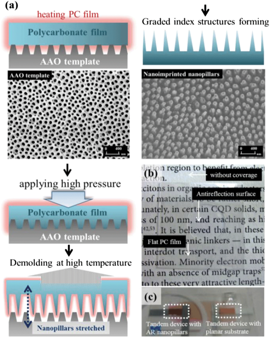
In the imprinting process, the prepared PC film is thermally-nanoimprinted by a nanoporous anodized aluminum oxide (AAO) template. The diameter of the nanoholes of AAO is about 150 nm. Its SEM image is shown in Fig. 2(a). The imprinted AR nanostructure was made on the bottom side of the PC film, which is about 200 μm-thick. The PC film was heated in a steel chamber with both top and bottom hot plates at a temperature higher than the glass transition temperature of polycarbonate (about 170 °C). The heated PC film was imprinted by an AAO template to form the antireflection nanopillars. To have a uniform air pressure on the PC film, a thin polyethylene terephthalate (PET) film was placed on the PC film and sealed by the steel chamber. The air pressure in the chamber was increased to 25 kg cm−2 so that the nanopores in the AAO were filled with molten polycarbonate. After five minutes of imprinting, the whole system was cooled down to a specified temperature (30, 50, 70, 100, 150 °C) and the air pressure was released. Then the AAO template was demolded immediately. Tapered nanopillars were formed on the PC film surface after the removal of the AAO template. The remaining aluminum layer was dissolved in a chromic acid solution for 3 hours. In general, applying a higher pressure and a longer imprint time increase the average height of the nanopillars and gives better AR effects. But these also make the AAO template tightly stick to the PC substrate and lead to damage of the transferred PC patterns during the demolding process. The optimized imprint pressure was ∼25 kg cm−2 at a temperature of 170 °C. We also increased the demolding temperature to further stretch the nanopillars by the friction force of the demolding process. More tapered nanopillars were formed due to the viscous effect of the PC film near the melting temperature.
 | ||
| Fig. 2 (a) The thermal nanoimprint process with the AAO template. Pictures of (b) a paper and (c) the bifunctional devices covered with the patterned PC film under a bright light source. | ||
Fig. 2(b) and (c) show pictures of the imprinted films taken by a CCD camera under bright light illumination. The light source was a 60 W incandescent lamp set in front of the paper and the tandem devices. Obviously, a darker image was observed for the nanopillars due to the antireflection effect.
Fig. 3 shows AFM images of the nanopillars under different fabrication conditions. It can be seen that the nanopillars did not follow the cylindrical profiles of the AAO nanopoles. They formed tapered shapes with an irregular distribution. As shown in Fig. 4(a), we found that the average height of the nanopillars was linearly proportional to the pressure applied. Moreover, we increased the demolding temperature and stretched the nanopillars using the friction force of the demolding process. A tapered surface morphology and higher nanopillars were found when the demolding temperature was higher. To check the antireflection properties of the tapered nanopillar structures, we measured the reflection spectra of PC films with and without nanostructures. Fig. 4(b) shows the average reflectivity of films with imprinted nanopillars with different average heights. The diameter of the nanopillars was 150 nm and the average height was determined by the imprinting pressure. The referenced light was incident on the sample in the normal direction, and the reflected light was measured by an integral sphere. The reflectance decreased with increasing average height. When we increased the demolding temperature to stretch the nanopillars, a more rapid decrease of average reflectance was found due to the more tapered surface morphology. Compared with the flat PC film, the average reflectivity of the patterned PC substrate was reduced from 10.2% to 3.3% in our most optimized case.
 | ||
| Fig. 3 Thermal nanoimprint results of PC films with an AAO template under different imprinting pressures and demolding conditions: (a) 5 kg cm−2, (b) 15 kg cm−2, (c) 25 kg cm−2 for room temperature demolding and (d) 25 kg cm−2 for high temperature demolding. | ||
 | ||
| Fig. 4 (a) Average height of nanopillars under different imprinting pressures and demolding temperatures. (b) Average reflectivity in the visible spectrum (400 nm–800 nm) of different AR nanopillars. | ||
Results and discussion
Comparing the J–V characteristics of the tandem device and a reference top-emission OLED (TOLED) in Fig. 5(a), it is found that the current density of the tandem device is slightly lower than the TOLED. This is due to the increased series resistance from the tandem OPV structure. In addition, the current efficiency is lower due to the strong absorption of the OPV component, as shown in Fig. 5(b). The current efficiency decreased from 3.4 cd A−1 to 1.78 cd A−1, which is about a 53.2% loss. After applying AR nanopillars on the tandem device to extract the light confined in the high-index organic layers, the luminance was improved by 43.3%. A picture of the tandem device partially covered with AR nanopillars is shown in the inset of Fig. 5(a), in which an obvious increase of the brightness can be observed. It is noted that the nanopillars have a broadband antireflection behavior. This indicates that the extraction enhancement is the same for different wavelengths. The emitting spectra would not be modified by these nanostructures. The peak wavelength was the same at 530 nm as shown in Fig. 5(c). There is no distortion in the color emitted. | ||
| Fig. 5 (a) Current density vs. voltage characteristics (inset: an image of the tandem device pixel partially covered with AR nanopillars), (b) current efficiency vs. current density curves and (c) emission spectra of the TOLED and bifunctional devices (in electroluminance-mode). | ||
Fig. 6 shows the J–V characteristics of the bifunctional device and a reference organic solar cell operated in the OPV mode under dark and light illumination conditions. The short circuit current density (JSC), open circuit voltage (VOC), fill factor (FF), and power conversion efficiency (PCE) of the bifunctional device and the reference OPV device are shown in Fig. 6. Under AM 1.5G 1-sun solar illumination, the bifunctional device gives the following performance for: short circuit current density: 1.1 mA cm−2, open circuit voltage: 1.03 V, fill factor: 42.79%, and has a power conversion efficiency of 0.48%. After integrating the AR nanopillars on the device, the power conversion efficiency was increased from 0.48% to 0.61% under irradiation from the normal direction, which is a 27.0% improvement. The improvement in PCE comes mainly from the higher short circuit current density, while the open circuit voltage remains the same with AR nanopillars. This demonstrates that the improvement in conversion efficiency is attributed to more injected light being coupled into the device by using the AR nanopillars. The relative enhancement ratios of the luminous and conversion efficiencies as a function of the incident angle are shown in Fig. 7 for the bifunctional devices covered with the AR nanopillars. The improvement in luminance becomes more significant at larger incident angles with a maximum improvement of 79.7% at 50°. In addition, the conversion efficiency ratio is enhanced at larger incident angles. It reached as high as a 44.4% relative improvement, which was due to better light transmittance and a larger effective light path at large incident angles.27
 | ||
| Fig. 6 Current density vs. voltage of the bifunctional devices with and without AR nanopillars and a reference organic solar cell, in darkness and under AM 1.5 illumination (under photovoltaic-mode operation). | ||
 | ||
| Fig. 7 Luminance and conversion efficiency enhancement ratios of the bifunctional devices with and without AR nanopillars. | ||
Increasing image contrast is another important application for this bifunctional device. In order to check the contrast enhancement, we measured the device characteristics under dark and bright conditions. The results are shown in Fig. 8. By comparing the device with the reflectance spectra of a reference device with a glass substrate, we found that reflectance between air and the glass substrate was the major problem limiting transparency in the visible wavelength. After attaching the nanopillars onto the device to reduce the ambient reflection on the substrate surface, the average reflectivity was decreased from 12.1% to 5.1%. Moreover, the luminous enhancement achieved by the additional light extraction from the device substrate can further increase the contrast ratio under bright ambient conditions. Fig. 8(b) shows the contrast ratio of devices driven by different operation voltages under normal indoor lighting. Generally, the contrast ratio in display applications can be expressed as28
 | (1) |
 | ||
| Fig. 8 Reflectance spectra (a) and contrast ratio (b) of reference TOLED and bifunctional devices with and without AR nanopillars. | ||
Conclusions
We reported a simple and inexpensive method to optimize the performance of the tandem device by using nanoimprinted AR nanopillars. The nanopillars were made on flexible polycarbonate substrates by using the nanoimprinting method with an anodized aluminum oxide template. The average reflectivity of the patterned polycarbonate substrate at visible wavelengths was reduced to 3.3% in the most optimized case. The AR nanopillars increased both the luminance and power conversion efficiency. With the AR nanopillars attached, the luminance and conversion efficiency were improved by 41.9% and 27.0%, respectively at normal incidence. Moreover, the contrast ratio was also increased up to 3.5 times.Acknowledgements
This work was supported by National Science Council, Taipei, Taiwan, under Contract no. NSC-101-2627-E-002-005, NSC-100-2120-M-007-006 and NSC-100-2221-E-001-010-MY3.Notes and references
- C. Tang and S. VanSlyke, Appl. Phys. Lett., 1987, 51, 913 CrossRef CAS PubMed.
- S. Reineke, F. Lindner, G. Schwartz, N. Seidler, K. Walzer, B. Lüssem and K. Leo, Nature, 2009, 459, 234–238 CrossRef CAS PubMed.
- G. H. Gelinck, H. E. A. Huitema, E. van Veenendaal, E. Cantatore, L. Schrijnemakers, J. B. van der Putten, T. C. Geuns, M. Beenhakkers, J. B. Giesbers and B.-H. Huisman, Nat. Mater., 2004, 3, 106–110 CrossRef CAS PubMed.
- P. Peumans, V. Bulovic and S. Forrest, Appl. Phys. Lett., 2000, 76, 2650–2652 CrossRef CAS PubMed.
- C.-J. Yang, T.-Y. Cho, C.-L. Lin and C.-C. Wu, Appl. Phys. Lett., 2007, 90, 173507 CrossRef PubMed.
- C.-Y. Yang, T.-Y. Cho, Y.-Y. Chen, C.-J. Yang, C.-Y. Meng, C.-H. Yang, P.-C. Yang, H.-Y. Chang, C.-Y. Hsueh and C.-C. Wu, Appl. Phys. Lett., 2007, 90, 233512 CrossRef PubMed.
- H. Okada, S. Naka, Y. Matsushita, H. Shimada, J. Yanagi, M. Shibata and H. Onnagawa, Jpn. J. Appl. Phys., 2007, 46, 1328 CrossRef CAS.
- H. Kang, G. Kim, I.-W. Hwang, Y. Kim, K. C. Lee, S. H. Park and K. Lee, Sol. Energy Mater. Sol. Cells, 2012, 107, 148–153 CrossRef CAS PubMed.
- J. Xue and S. R. Forrest, Appl. Phys. Lett., 2003, 82, 136–138 CrossRef CAS PubMed.
- X. Z. Wang, H. L. Tam, K. S. Yong, Z.-K. Chen and F. Zhu, Org. Electron., 2011, 12, 1429–1433 CrossRef CAS PubMed.
- T. Yamasaki, K. Sumioka and T. Tsutsui, Appl. Phys. Lett., 2000, 76, 1243–1245 CrossRef CAS PubMed.
- J. Lim, S. S. Oh, D. Y. Kim, S. H. Cho, I. T. Kim, S. Han, H. Takezoe, E. H. Choi, G. S. Cho and Y. H. Seo, Opt. Express, 2006, 14, 6564–6571 CrossRef.
- Y. Sun and S. R. Forrest, Nat. Photonics, 2008, 2, 483–487 CrossRef CAS.
- Y. R. Do, Y. C. Kim, Y. W. Song, C. O. Cho, H. Jeon, Y. J. Lee, S. H. Kim and Y. H. Lee, Adv. Mater., 2003, 15, 1214–1218 CrossRef CAS.
- J. M. Ziebarth, A. K. Saafir, S. Fan and M. D. McGehee, Adv. Funct. Mater., 2004, 14, 451–456 CrossRef CAS.
- Y.-H. Ho, K.-Y. Chen, K.-Y. Peng, M.-C. Tsai, W.-C. Tian and P.-K. Wei, Opt. Express, 2013, 21, 8535–8543 CrossRef CAS PubMed.
- K. Saxena, D. S. Mehta, V. K. Rai, R. Srivastava, G. Chauhan and M. N. Kamalasanan, J. Lumin., 2008, 128, 525–530 CrossRef CAS PubMed.
- Y.-H. Ho, C.-C. Liu, S.-W. Liu, H. Liang, C.-W. Chu and P.-K. Wei, Opt. Express, 2011, 19, A295–A302 CrossRef PubMed.
- X.-X. Fu, X.-N. Kang, B. Zhang, C. Xiong, X.-Z. Jiang, D.-S. Xu, W.-M. Du and G.-Y. Zhang, J. Mater. Chem., 2011, 21, 9576–9581 RSC.
- K. Forberich, G. Dennler, M. C. Scharber, K. Hingerl, T. Fromherz and C. J. Brabec, Thin Solid Films, 2008, 516, 7167–7170 CrossRef CAS PubMed.
- W. Luk, K. Yeung, K. Tam, K. Ng, K. Kwok, C. Kwong, A. Ng and A. Djurišíć, Org. Electron., 2011, 12, 557–561 CrossRef CAS PubMed.
- D. Chen, Sol. Energy Mater. Sol. Cells, 2001, 68, 313–336 CrossRef CAS.
- P. Clapham and M. Hutley, Nature, 1973, 244, 281–282 CrossRef.
- J.-Q. Xi, M. F. Schubert, J. K. Kim, E. F. Schubert, M. Chen, S.-Y. Lin, W. Liu and J. A. Smart, Nat. Photonics, 2007, 1, 176–179 CAS.
- K. Choi, S. H. Park, Y. M. Song, Y. T. Lee, C. K. Hwangbo, H. Yang and H. S. Lee, Adv. Mater., 2010, 22, 3713–3718 CrossRef CAS PubMed.
- X. Li, X. Yu and Y. Han, J. Mater. Chem. C, 2013, 1, 2266–2285 RSC.
- Y. Wang, R. Tummala, L. Chen, L. Q. Guo, W. Zhou and M. Tao, J. Appl. Phys., 2009, 105, 103501 CrossRef PubMed.
- Z. Wu, L. Wang and Y. Qiu, Opt. Express, 2005, 13, 1406–1411 CrossRef CAS.
| This journal is © The Royal Society of Chemistry 2014 |