Enhanced efficiency of polymer solar cells by incorporated Ag–SiO2 core–shell nanoparticles in the active layer
Wenfei Shena,
Jianguo Tang*a,
Renqiang Yang*b,
Hailin Conga,
Xichang Baob,
Yao Wanga,
Xinzhi Wanga,
Zhen Huanga,
Jixian Liua,
Linjun Huanga,
Jiqing Jiaoa,
Qingsong Xua,
Weichao Chenb and
Laurence A. Belfiore*ac
aInstitute of Hybrid Materials, The Growing Base for State Key Laboratory, Qingdao University, 308 Ningxia Road, Qingdao 266071, P. R. China. E-mail: jianguotangde@hotmail.com
bQingdao Institute of Bioenergy and Bioprocess Technology, Chinese Acadamy of Sciences, 189 Songling Road, Qingdao, 266101, P. R. China. E-mail: yangrq@qibebt.ac.cn
cDepartment of Chemical and Biological Engineering, Colorado State University, Fort Collins, Colorado 80523, USA. E-mail: belfiore@engr.colostate.edu
First published on 29th November 2013
Abstract
In this article, we creatively incorporated Ag–SiO2 core–shell nanoparticles (Ag–SiO2-NPs) into photo-/electro-active layers consisting of poly(3-hexylthiophene) (P3HT) and phenyl-C61-butyric acid methyl ester (PCBM) in polymer solar cells (PSCs). By this way, the photovoltaic performances of PSCs have largely been enhanced. The results demonstrate a 13.50% enhancement of short-circuit photocurrent density (Jsc) and a 15.11% enhancement of power conversion efficiency (PCE) as the weight percent of doped Ag–SiO2-NPs is 1.5 wt% in the active layer of corresponding PSCs. We attribute the enhancement to the localized surface plasmon resonance (LSPR) effect of Ag–SiO2-NPs, by which the incident light harvesting is enlarged. Whereas, the incorporated bare Ag nanoparticles (Ag-NPs) in the active layer of PSCs decreases the PCE, which is ascribed to the quenching of excitons at the surface of Ag-NPs and the poor dispersion of Ag-NPs in the active layer. Importantly, this work provides a new approach to enhance the performance of PSCs via the LSPR effect of Ag–SiO2-NPs other than via non-circular nanometals.
1 Introduction
Bulk heterojunction (BHJ) polymer solar cells (PSCs) based on conjugated polymers/fullerene derivatives show great potential in solar energy conversion systems by virtue of their unique characteristics, such as low cost, easy fabrication at ambient temperature, semi-transparency, and mechanical flexibility.1,2 Up to now, the reported power conversion efficiency (PCE) of BHJ-PSCs can reach to 6–8%,3–9 but it is much lower than that of inorganic solar cells. In the modules of current BHJ-PSCs devices, P3HT:PCBM combination as electron-donor/acceptor system is popular,10–14 whose PCE being reported is up to 5%.11,15,16 In fact, the prime restriction is the weak light absorption of active layer in PSCs.17 Although the thicker active layer may improve light absorption, it deteriorates the charge carrier efficiency because of the small degree of crystallinity in PSCs.18A metal nanoparticle can act as an antenna capable of increasing both the excitation rate and quantum yield of a fluorophore in close proximity to the nanoparticle, via its localized surface plasmon resonance (LSPR).
The electromagnetic (EM) field of the incident light near the surface of metallic nanoparticles (MNP) is amplified,19,20 when the electric field frequency of the incident light resonates with the oscillation of the MNP conduction electrons.21 This property thus enhances the charge carrier concentration of organic fluorophore and yields a PCE increase. Due to the tunability of LSPR, it becomes one of the best candidates for enhancing the optical absorption of the active layer.14,22–25 The published papers indicated the incorporation of MNPs into PSCs either on the top of indium tin oxide (ITO),26,27 within hole transport layer of poly(3,4-ethyl-enedioxythiophene):poly(styrenesulfonate) (PEDOT:PSS),23,28–30 or within the interconnecting layer of tandem solar cell.31 Recently, anomalous increase12,14 and decrease32,33 in PCE have been reported by incorporating metallic NPs into the active layer. W. C. H. Choy12 demonstrated an enhancement of PCE by incorporating naked silver NPs with different shapes into active layer. In contrast, D. S. Ginger33 found that silver nanoprisms accumulate long-live negative charges when they are in contact with P3HT:PCBM blend, which caused metal-mediated losses in PSCs. While, the recently published work of Vo-Van Truong34 revealed that the PCE of devices with thin active layer was enhanced by 27% due to the plasmonic effect induced by the presence of gold nanorods in active layer, its value was lowered in the devices made with the thicker active layer. As far as we know, we believe that the MNPs embedded in the active layer of PSCs is better for light absorption than that embedded in other layers, because the magnified electromagnetic field near the particle surface is strongest, and embedding MNPs directly in active layer will benefit energy transfer from MNPs to organic conjugate electro-active polymers.35 In addition, incorporated NPs in the active layer would increase the optical path and improve the light absorption within the absorbing layer via their scattering effect of incident light in the intrinsic absorbing layer. Therefore, embedding metallic NPs in active layer of PSCs will achieve better light absorption. The silica shell around the silver core plays the inert spacer to separate the direct contact between chemical active silver core and the conjugate fluorophore and to adjust the distance between them to be optimal range of 10–25 nm.36 With the same concept, Y. Yang37 etc. incorporated Au–SiO2 core–shell nanorod into the active layer of the polymer solar cell to improve its performance. Besides, Q. Wang38 etc. demonstrated an enhancement of PCE of PSCs by incorporating Au–SiO2 core–shell NPs. Considering the relatively low price and easy fabrication of Ag–SiO2 core–shell NPs compared with that of Au–SiO2, we expect that Ag–SiO2 core–shell NPs can serve as an additive of PSCs in the industrialised products of future.
In this study, we expected to enhance the performance of PSCs by incorporating Ag–SiO2 core–shell nanoparticles (Ag–SiO2-NPs) into poly(3-hexylthiophene):phenyl-C61-butyric acid methyl ester (P3HT:PCBM) layer. We systematically investigated the glaring discrepancies between incorporating Ag–SiO2-NPs and Ag-NPs and demonstrated the enhance effects of Ag–SiO2-NPs on short-circuit photocurrent density (Jsc), power conversion efficiency (PCE) and EQE values. The effectiveness of Ag–SiO2-NPs is ascribed to their LSPR to transfer the additional light energy to P3HT:PCBM active layer in PSCs.
2 Experimental
2.1 Syntheses of Ag-NPs and Ag–SiO2-NPs
Ag–SiO2-NPs and Ag-NPs were prepared according to our previously reported methods in ref. 39. In order to increase the hydrophobicity, Ag–SiO2-NPs was treated with gamma-glycidoxypropyltrimethoxysilane (KH560, 50 vol% aqueous solution). 1 ml KH560 aqueous solution was added to the 10 ml Ag–SiO2-NPs sol–gel solution, and the pH of the solution was adjusted to 8 with dilute ammonia aqueous solution and NPs solution was treated for 12 h at room temperature. The obtained Ag–SiO2-NPs were purified for 3 times by centrifugation with ethanol to remove the residual chemicals, the Ag–SiO2-NPs were dried in a vacuum drying chamber at a low temperature. Ag-NPs were purified and dried with the same method.2.2 Fabrication of PSCs
We selected poly(3-hexylthiophene) (P3HT, 98% regioregularity, luminescence Ch) and phenyl-C61-butyric acid methyl ester (PCBM, 99.5%, American Dye Sources Inc) as photovoltaic materials. The device structure of polymer solar cells in this work is shown as the following module: glass/ITO/poly(3,4-ethyl-enedioxythiophene):poly(styrenesulfonate) (PEDOT:PSS)/poly(3-hexylthiophene):phenyl-C61-butyric acid methyl ester (P3HT:PCBM)/Ca/Al.1 Fig. 1 shows the schematic diagram of PSCs. The details of fabrication processes are shown as follows: | ||
| Fig. 1 Schematic of normal structure polymer solar cell with Ag–SiO2-NPs or Ag-NPs in the active layer, glass/ITO/PEDOT:PSS/P3HT:PCBM:NPs/Ca/Al. | ||
ITO-coated glass substrates with a nominal sheet resistance of 15 Ω sq−1 were ultrasonically cleaned with detergent, de-ionized water, acetone and iso-propyl alcohol for 20 min in each round, and subsequently dried in an oven at 110 °C.25,29 The substrates were treated in a UV ozone chamber for 6 min prior to the deposition of the hole selective materials. The PEDOT:PSS solution (Clevios PVP Al4083, HC Starck) was spin-coated at 4000 rpm for 30 s to form a hole transport layer and then annealed at 150 °C for 20 min. The thickness of the PEDOT:PSS film was about 50 nm. To change the concentration of Ag–SiO2-NPs in the active layer, different weight of Ag–SiO2-NPs was added to P3HT:PCBM (1![[thin space (1/6-em)]](https://www.rsc.org/images/entities/char_2009.gif) :1) chlorobenzene solution of 30 mg ml−1. The blend solution was fully mixed by ultrasonics. Ag-NPs was mixed in P3HT:PCBM chlorobenzene solution by the same method. The substrates with PEDOT:PSS and blend solutions were then transferred into a nitrogen-filled glove box, and the P3HT:PCBM (1:1) chlorobenzene solutions were spin-coated on PEDOT:PSS layer at 1000 rpm for 40 seconds to form ∼150 nm thick active layers. The device fabrication parameters were optimized prior to this preparation of PSC. The fabricated PSC active layer was then subjected to thermal annealing at 150 °C for 10 min. The thickness of the active layer is about 150 nm. At last, Ca/Al electrodes were thermally evaporated onto the active layer with a thickness of 5 nm and 100 nm respectively, to form a cathode, at a vacuum (≤10−6 Torr) condition.
:1) chlorobenzene solution of 30 mg ml−1. The blend solution was fully mixed by ultrasonics. Ag-NPs was mixed in P3HT:PCBM chlorobenzene solution by the same method. The substrates with PEDOT:PSS and blend solutions were then transferred into a nitrogen-filled glove box, and the P3HT:PCBM (1:1) chlorobenzene solutions were spin-coated on PEDOT:PSS layer at 1000 rpm for 40 seconds to form ∼150 nm thick active layers. The device fabrication parameters were optimized prior to this preparation of PSC. The fabricated PSC active layer was then subjected to thermal annealing at 150 °C for 10 min. The thickness of the active layer is about 150 nm. At last, Ca/Al electrodes were thermally evaporated onto the active layer with a thickness of 5 nm and 100 nm respectively, to form a cathode, at a vacuum (≤10−6 Torr) condition.
2.3 Characterization
The transmission electron microscopy (TEM) images of Ag-NPs and Ag–SiO2-NPs were obtained on a JEM-2000 Ex. Size distribution of Ag-NPs and Ag–SiO2-NPs were obtained by Microtrac particle size analyzer. The current density–voltage (J–V) characteristics were measured under AM 1.5 solar illumination at an intensity of 100 mW cm−2 with Newport solar simulator by a Keithley 2420 source measurement in air. The scanning electron microscopy (SEM) images of the doped P3HT:PCBM films by Ag-NP or Ag–SiO2-NPs were measured by a FE-SEM Hitachi S-4800. Atomic force microscopy (AFM) measurements were carried out on an Agilent 5400 AFM at ambient temperature. The X-ray diffraction (XRD) spectra were taken by a Mac Science, equipped with Cu Kα source. The UV-Vis absorption spectra of pristine P3HT:PCBM film and P3HT:PCBM films with Ag–SiO2-NPs or Ag-NPs were taken on a Varian Cary 50 UV-Vis spectrometer. The thickness of P3HT:PCBM films was acquired using a Veeco Dektak 150 surface profiler. The external quantum efficiencies (EQE) of PSCs were analyzed using a certified Newport incident photon conversion efficiency (IPCE) measurement system.3 Results and discussion
The TEM images of synthesized Ag-NPs and Ag–SiO2-NPs are shown in Fig. 2. In Fig. 2a and b, the diameter of Ag-NPs is about 20 nm and the thickness of silica shell of Ag–SiO2-NPs is about 15 nm, while in Fig. 2c, the magnified image of Ag–SiO2-NPs indicates the porous structure of silica shell with about 1 nm pore diameters. There is a publication that porous structure40 benefits the light transmittance through the shell, and thereby the shell does not screen the enhanced electromagnetic (EM) field of Ag–SiO2-NPs to be transferred outside. Fig. 2d and e show the size distribution of Ag-NPs and Ag–SiO2-NPs, we can see that Ag-NPs show a relative narrow size distribution and the size distribution of Ag–SiO2-NPs becomes larger after silica encapsulation. | ||
| Fig. 2 The TEM images of (a) the size-controllable Ag-NPs, (b) the core–shell structure Ag–SiO2-NPs synthesized by wet-chemistry approach, the magnified TEM image of Ag–SiO2-NPs; size distributions of Ag-NPs (d) and Ag–SiO2-NPs (e). | ||
To investigate the changes of photo-/electro-characteristics caused by the silica shell of Ag–SiO2-NPs, the absorption spectra of Ag–SiO2-NPs and Ag-NPs were measured, as shown in Fig. 3. The result indicates the significant red shift of the maximum absorption peaks from 426 nm to 439 nm because of SiO2 encapsulation around Ag-core in Ag–SiO2-NPs, which makes Ag–SiO2-NPs absorbs more visible light. On the other hand, the width of absorption peak of Ag–SiO2-NPs at half-height is larger than that of Ag-NPs. These spectra characteristics promise a better absorption performance. Therefore, they will definitely enhance the light absorption property of P3HT:PCBM blend in PSCs when Ag–SiO2-NPs is incorporated into this active layer. B. Gu35 also reported the porous shell of Ag–SiO2-NPs and Rhodamine 6G (R6G) molecules diffused into porous shell of Ag–SiO2-NPs. He confirmed that Raman scattering (SERS) enhancement effect of Ag–SiO2-NPs is higher than that of Ag-NPs. These incidences revealed Ag–SiO2-NPs could serve as novel additive for organic photo-/electro-active components. In this work, the different weight percent of Ag–SiO2-NPs was incorporated into the active layer of P3HT:PCBM. The optimized PSC performance with various concentrations of Ag–SiO2-NPs in the active layers was shown in Table 1, and the corresponding current density–voltage (J–V) characteristics under illumination were shown in Fig. 4. The results demonstrate the concentration of Ag–SiO2-NPs effect on the performance of PSCs. At low concentration (i.e., 0.75 wt% Ag–SiO2-NPs), the Jsc of the PSCs increases to 9.06 mA cm−2 from 8.37 mA cm−2, and PCE increases to 3.62% from 3.44%, compared with the optimized reference device. At high concentration (i.e., 5 wt% Ag–SiO2-NPs), the Jsc of PSCs dramatically decreases to 7.51 mA cm−2, and PCE decrease to d 2.25%.
 | ||
| Fig. 3 The UV-Vis absorption spectra of Ag-NPs and Ag–SiO2-NPs in water. | ||
| Device | Voc (V) | Jsc (mA cm−2) | FF (%) | PCE (%) |
|---|---|---|---|---|
| Reference device | 0.63 | 8.37 | 64.81 | 3.44 |
| 0.75 wt% Ag–SiO2-NPs device | 0.64 | 9.06 | 62.08 | 3.62 |
| 1.5 wt% Ag–SiO2-NPs device | 0.64 | 9.50 | 64.85 | 3.96 |
| 3 wt% Ag–SiO2-NPs device | 0.62 | 9.20 | 62.42 | 3.52 |
| 5 wt% Ag–SiO2-NPs device | 0.64 | 7.51 | 45.74 | 2.25 |
 | ||
| Fig. 4 Current density–voltage (J–V) characteristics of PSCs with different incorporated Ag–SiO2-NPs concentrations in active layer. | ||
It is easy to see (Table 1) the optimal Ag–SiO2-NPs concentration in the active layer is 1.5 wt%, at which the Jsc and PCE of PSC reach to the maximum values at 9.50 mA cm−2 and 3.96%, respectively. Accordingly, as the concentration was set at 3%, the lower Jsc and PCE of the PSC are 9.20 mA cm−2 and 3.52%, respectively. The Jsc values of devices with 0.75 wt%, 1.5 wt%, 3 wt% Ag–SiO2-NPs show various enhancements compared with that of reference devices, and we accredit to that the enhancement is caused by the increased light absorption induced by the LSPR effect of Ag–SiO2-NPs. However, it is not hard to see that the Jsc values of devices do not increase with the increase of Ag–SiO2-NP concentration in PSCs but decrease at higher concentration. We believe that excessively incorporated Ag–SiO2-NPs will occupy the domain place of conjugate polymer, thus cause the Jsc value decreases relatively. The Voc values of Ag–SiO2-NP doped devices remain similar to reference devices as the concentration varies from 0.75 wt% to 5 wt%, which demonstrates that the incorporation of Ag–SiO2-NPs would not bring in new excited energy levels in the P3HT:PCBM system. The optimal fill factor (FF) of PSC device at optimal Ag–SiO2-NPs concentration (1.5 wt%) is 64.81%, but it goes down dramatically to 45.74% when the concentration of Ag–SiO2-NPs is up to 5 wt%, which demonstrates that the excessive incorporation of Ag–SiO2-NPs deteriorates the interpenetrating structure between P3HT and PCBM in active layer of PSCs.41 It is well known that the FF is closely related to series resistance of the photovoltaic device. In our devices, the FF of the device with 1.5 wt% Ag–SiO2-NPs is equivalent to that of reference device without NPs, which demonstrates that the electrical property of PSCs can't be affected by the incorporation of Ag–SiO2-NPs. Our results are obviously different from that of V. V. Truong.34 V. V. Truong reported that the performance of Au nanorods doped devices decrease with thick active layer (∼100 nm), whereas the PCE performance of devices doped with Ag–SiO2-NPs remains higher value than that of reference devices even with 150 nm thick active layer. We believe that it is the exciton blocking effect of silica shell. Ag–SiO2-NPs homogeneously dispersed in the active layer and their plasmon effect works without affecting the electronic properties of devices. Hence, the devices with optimized concentrations of Ag–SiO2-NPs enhance the comprehensive performance of PSCs dramatically.
As comparison, the incorporation of Ag-NPs in the active layer of P3HT:PCBM blend has been investigated. When the addition of Ag-NPs is at 1.5 wt% in P3HT:PCBM blend, the Jsc, FF and PCE drastically decrease to 5.91 mA cm−2, 51.47% and 1.89%, respectively (Table 2). Fig. 5 shows the corresponding J–V characteristics under AM 1.5G illumination at 100 mW cm−2. The result shows that the added Ag-NPs in the active layer deteriorates the performance of PSCs significantly, even at optimized concentration of 1.5 wt%.
| Device | Voc (V) | Jsc (mA cm−2) | FF (%) | PCE (%) |
|---|---|---|---|---|
| Reference device | 0.63 | 8.37 | 64.81 | 3.44 |
| 1.5 wt% Ag-NPs device | 0.62 | 5.91 | 51.47 | 1.89 |
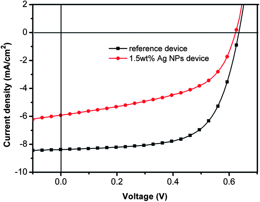 | ||
| Fig. 5 Current density–voltage (J–V) characteristics of the device with 1.5 wt% Ag-NPs in the active layer along with reference device. | ||
Based on the two-phase structure of interpenetrated P3HT and PCBM in nano-scale in active layer of PSCs, we conclude two factors that influence the efficiency of PSC. The first one is the improved dispersity status of Ag–SiO2-NPs in active layer by coated SiO2 shell. Fig. 6a and Fig. 6b show SEM top-view images of the active layer that contain 1.5 wt% Ag–SiO2-NPs and 1.5 wt% Ag-NPs. From Fig. 6a, one can see the unique dispersed Ag–SiO2-NPs in the active layer, which should scarcely deteriorate the two-phase structure of interpenetrated P3HT and PCBM in active layer of PSCs. However, the aggregated Ag-NPs, indicated in Fig. 6b, will seriously deteriorate the two-phase structure of interpenetrated P3HT and PCBM. The large aggregated particle can cut off the exciton transport tunnels that formed by interpenetrated continuous nano-phase network of P3HT and PCBM. Comparing the SEM and TEM images of NPs, one can see that size of Ag–SiO2-NPs is larger in SEM image than that shown in TEM image. The reason should be that after silica encapsulation and modification, the compatibility of NPs with polymer in active layer becomes better, thus, the absorbance of polymer chains on the surface of silica-encapsulated NPs makes the size of nanoparticles indicated by SEM image larger.
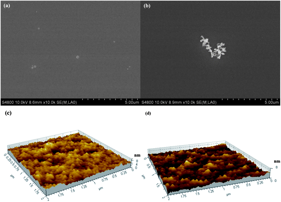 | ||
| Fig. 6 The SEM picture of P3HT:PCBM film with 1.5 wt% Ag–SiO2-NPs (a) and P3HT:PCBM film with 1.5 wt% Ag-NPs (b). 3D images of: pristine P3HT:PCBM (c) and P3HT:PCBM with 1.5 wt% Ag–SiO2-NPs (d). | ||
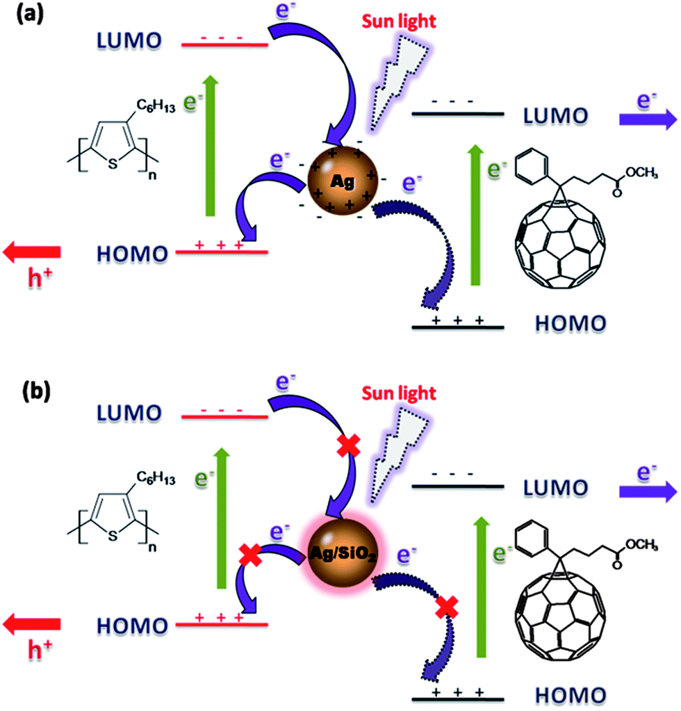
The second important factor should be that the coated SiO2 shell will prevent the excited electrons at silver nanoparticle surface transferring to active materials in PSCs. As shown in Fig. 8a, we believe that excited electrons in the outer orbit of silver atoms at the surface of silver nanoparticles may directly transfer to P3HT or PCBM in the vicinity of the nanoparticles, thus this process quenches the excitons in active layer. However, in the P3HT:PCBM: Ag–SiO2-NPs blend system, exciton quenching would be blocked by the SiO2 shell as in Fig. 8b, but the energy induced by the LSPR effect at silver nanoparticle surface can go through the thin porous SiO2 shell and transfer to P3HT:PCBM active material layer. So the energy transfer process from Ag–SiO2-NPs cores to photo-electric active materials is established instead of electron transfer process shown in Fig. 8a. At the same time, there are reports25,28,42 to support this point of view that incorporated bare metallic NPs in active layer should cause the exciton quenching.
Besides, the influence of incorporated nanoparticles on the morphological structure of active layer is also important to photovoltaic performance. We took AFM measurement to study the morphology changes after incorporating Ag–SiO2-NPs into active layer. Fig. 6c and d show the surface morphological structures of P3HT:PCBM active layer with or without Ag–SiO2-NPs. As a result, the root-mean-square roughness of pristine P3HT:PCBM film and the P3HT:PCBM film with 1.5 wt% Ag–SiO2-NPs are 1.16 nm and 1.28 nm, respectively, which indicates the incorporated Ag–SiO2-NPs in the active layer do not have obvious influence on the film morphology. Cheng-Si Tsao41 etc. incorporated ∼4 nm Cu2S nanoparticles to tune the phase separation in the P3HT:PCBM film. Based on the description of Heeger's publication,15 the thermal annealing has an enhancing effect on P3HT crystallization. In order to estimate the effect of Ag–SiO2 NPs on the crystallization of P3HT, the comparable results of the thermal annealing (curve b) and unannealing (curve b) samples were investigated by XRD measurements (Fig. 7). The increased intensity of the peak at 2θ ≈ 5° can be observed in annealing P3HT:PCBM layer. This is corresponding to the increased crystallization of P3HT.15 But there is weak intensity difference between pristine annealed P3HT:PCBM layer (curve b) and annealed P3HT:PCBM layer incorporated with Ag–SiO2-NPs (curve c). Therefore, we think that the incorporated Ag–SiO2-NPs will not affect the crystallization of P3HT. In conclude, we are sure that the improved performance is not caused by the changes of film morphology.
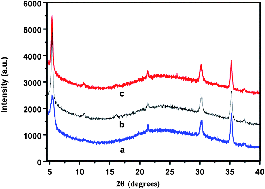 | ||
| Fig. 7 XRD patterns of unannealed P3HT:PCBM layer (curve a), annealed P3HT:PCBM layer (curve b) and P3HT:PCBM layer with Ag–SiO2-NPs (curve c). | ||
 | ||
| Fig. 8 (a) Schematic illustration of charge transfer mechanism between Ag-NPs and P3HT:PCBM blend; (b) schematic illustration of charge transfer mechanism been prevented by silica spacer outside Ag-NPs. | ||
In order to further investigate reasons that cause the performance discrepancy of PSCs incorporating Ag–SiO2-NPs and Ag-NPs, we took their absorption spectra. As shown in Fig. 9, the spectra shapes of P3HT:PCBM films incorporated by Ag–SiO2-NPs and Ag-NPs show small differences. The absorption intensity of P3HT:PCBM layer with 1.5 wt% Ag–SiO2-NPs is almost equal to that of P3HT:PCBM film with 1.5 wt% Ag-NPs, and their absorption intensities are obviously stronger than that of pristine P3HT:PCBM layer. In order to confirm the cause, the thicknesses of films were measured and the results were listed in Table 3. It is not difficult to see the film thicknesses of the pristine P3HT:PCBM, P3HT:PCBM with 1.5 wt% Ag–SiO2-NPs and P3HT:PCBM with 1.5 wt% Ag-NPs are 163 nm, 159 nm and 165 nm, respectively. Obviously, the additions of Ag–SiO2-NPs and Ag-NPs do not change the thicknesses of films. Hence, we certify that the enhancement of the absorptions corresponds to LSPR effect of metallic NPs, and it is easy to find that the PCE enhancement is caused by the enhanced light absorption of PSCs with Ag–SiO2-NPs.
 | ||
| Fig. 9 UV-Vis absorption spectra of pristine P3HT:PCBM film, 1.5 wt% Ag-NPs doped P3HT:PCBM film and 1.5 wt% Ag–SiO2-NPs doped P3HT:PCBM film. | ||
| Sample | Pristine P3HT:PCBM film | P3HT:PCBM film with 1.5 wt% Ag–SiO2-NPs | P3HT:PCBM film with 1.5 wt% Ag-NPs |
|---|---|---|---|
| Thickness (nm) | 163 | 159 | 165 |
The external quantum efficiency (EQE) can confirm the better photovoltaic efficiency of PSCs, which reaches 100% when all incident photons generate electron–hole excitons. However, EQE is obviously less than 100% which is caused by the reflection of incident light, weak absorption of polymers and the recombination of charge carriers in devices. The EQE of devices with 1.5 wt% Ag–SiO2-NPs, 1.5 wt% Ag-NPs and 0 wt% nanoparticles were measured respectively. As shown in Fig. 10a, although all shapes of EQE figures are similar, the EQE values are different obviously. The device with 1.5 wt% Ag–SiO2-NPs shows a maximal EQE value, and the device with 1.5 wt% Ag-NPs shows a minimal EQE value. Integrated photocurrent current curves (Fig. 10b) were calculated by the EQE curves.
 | ||
| Fig. 10 (a) The EQE spectra of PSCs with 1.5 wt% Ag–SiO2-NPs, 1.5 wt% Ag-NPs and the EQE spectra of reference PSC. (b) Photocurrent calculated from corresponding EQE curves and integrated photocurrent densities of corresponding devices. | ||
The integrated photocurrent densities of devices with 1.5 wt% Ag–SiO2-NPs, 1.5 wt% Ag-NPs and 0% nanoparticles are 9.39, 8.09 and 5.66 mA cm−2, which are in good agreement with the measured photocurrent densities of 9.50, 8.37 and 5.91 mA cm−2, respectively. There are about 5% errors between integrated current densities and measured current densities, which is the consequence of the spectra mismatch between xenon lamp and sun. Compare the result of UV-vis spectra and EQE curves, it's interesting to find that the relatively stronger light absorption of devices with 1.5 wt% Ag-NPs does not lead to higher EQE values. Considering EQE values are mainly determined by light absorption and charge carries recombination, we are sure that Ag-NPs caused much more charge carries recombination in devices. Hence, we further testify that incorporating Ag-NPs in the devices would cause excitons quenching, and incorporating Ag–SiO2-NPs would not cause excitons quenching, and we can conclude that the observed absorption enhancement via LSPR effects contributes significantly to the enhancement of Jsc, EQE and PCE. It's worthy to note that incorporated Ag–SiO2-NPs other than bare Ag-NPs in the active layer achieving an PCE enhancement of 15.11%. Most importantly, our work contributes to a new approach of using metallic NPs to increase the PCE of PSCs.
All in all, Ag–SiO2-NPs exhibit great advantages for application in polymer solar cells: (1) the transparence dielectric silica spacer in Ag–SiO2-NPs prevents the charge transfers between Ag-NPs and active layer of P3HT:PCBM, and thus provide the structural environment to keep the high efficient transfer of plasmon energy of Ag-NPs to active layer of P3HT:PCBM; (2) the dispersion of Ag–SiO2-NPs in the active layer is obviously better than that of Ag-NPs due to the capsulation of SiO2 around the silver nanoparticles, which keeps the perfect interpenetrating network between P3HT and PCBM nano-phases that is the necessary structure of BHJ-PSCs; (3) the synthesis of Ag–SiO2-NPs is easy and inexpensive, which is good for the industrialization of PSCs.
4 Conclusions
Considering the very thin active layer in polymer solar cells, efficient light absorption of active layer is critical for high photovoltaic performances. In this paper, a PCE enhancement of 15.11% in the PSCs has been achieved by incorporating Ag–SiO2-NPs into the active layer of solar cells. The intensity of light absorption in the P3HT:PCBM films with 1.5 wt% Ag–SiO2-NPs increased significantly as a result of LSPR induced localized electromagnetic field enhancement. Moreover, the discrepancy between incorporating Ag-NPs and Ag–SiO2-NPs were discussed. The performance of devices with 1.5 wt% (optimized concentration) Ag-NPs decreased dramatically compared with that of control devices, and we ascribe the decrease to the quenching of excitons and the poor dispersibility of Ag-NPs in P3HT:PCBM film. We believe that the result of this study provides an easy approach of using MNPs to enhance the performance of PSCs, and this might be applied to the commercial process of PSCs.Acknowledgements
The authors appreciate the financial supports from: (1) The National One-Thousand Foreign Expert Program (WQ20123700111); (2) Natural Scientific Foundation of China, Grant #51273096; (3) Natural Scientific Foundation of China, Grant #51373081; (4) International Collaborative Program of Qingdao Science & Technology Bureau, Grant #10-1-4-97-hz; (5) Shandong Province Project: Tackle Key Problem in Key Technology, #2010GGX10327; (6) program of Qingdao Science & Technology, #12-1-4-2-(8)-jch.Notes and references
- S. Gunes, H. Neugebauer and N. S. Sariciftci, Chem. Rev., 2007, 107, 1324–1338 CrossRef PubMed.
- P. G. Nicholson and F. A. Castro, Nanotechnology, 2010, 21, 492001 CrossRef PubMed.
- Z. He, C. Zhong, X. Huang, W. Y. Wong, H. Wu, L. Chen, S. Su and Y. Cao, Adv. Mater., 2011, 23, 4636–4643 CrossRef CAS PubMed.
- Z. He, C. Zhong, S. Su, M. Xu, H. Wu and Y. Cao, Nat. Photonics, 2012, 6, 593–597 CrossRef CAS.
- J. H. Seo, A. Gutacker, Y. Sun, H. Wu, F. Huang, Y. Cao, U. Scherf, A. J. Heeger and G. C. Bazan, J. Am. Chem. Soc., 2011, 133, 8416–8419 CrossRef CAS PubMed.
- R. Service, Science, 2011, 332, 293 CrossRef CAS PubMed.
- T. Yang, M. Wang, C. Duan, X. Hu, L. Huang, J. Peng, F. Huang and X. Gong, Energy Environ. Sci., 2012, 5, 8208 CAS.
- B. Ray, P. R. Nair and M. A. Alam, Sol. Energy Mater. Sol. Cells, 2011, 95, 3287–3294 CrossRef CAS PubMed.
- J. U. Lee, J. W. Jung, T. Emrick, T. P. Russell and W. H. Jo, Nanotechnology, 2010, 21, 105201 CrossRef PubMed.
- M. T. Dang, L. Hirsch and G. Wantz, Adv. Mater., 2011, 23, 3597–3602 CrossRef CAS.
- G. Li, V. Shrotriya, J. Huang, Y. Yao, T. Moriarty, K. Emery and Y. Yang, Nat. Mater., 2005, 4, 864–868 CrossRef CAS.
- X. Li, W. C. H. Choy, H. Lu, W. E. I. Sha and A. H. P. Ho, Adv. Funct. Mater., 2013, 21, 2728–2735 CrossRef.
- W. E. I. Sha, W. C. H. Choy, Y. G. Liu and W. Cho Chew, Appl. Phys. Lett., 2011, 99, 113304 CrossRef PubMed.
- F.-X. Xie, W. C. H. Choy, C. C. D. Wang, W. E. I. Sha and D. D. S. Fung, Appl. Phys. Lett., 2011, 99, 153304 CrossRef PubMed.
- W. Ma, C. Yang, X. Gong, K. Lee and A. J. Heeger, Adv. Funct. Mater., 2005, 15, 1617–1622 CrossRef CAS.
- M. Reyes-Reyes, K. Kim and D. L. Carroll, Appl. Phys. Lett., 2005, 87, 083506 CrossRef PubMed.
- J.-M. Nunzi, C. R. Phys., 2002, 3, 523–542 CrossRef CAS.
- A. Moliton and J. M. Nunzi, Polymer Int., 2006, 55, 583–600 CrossRef CAS.
- M. L. Juan, M. Righini and R. Quidant, Nat. Photonics, 2011, 5, 349–356 CrossRef CAS.
- A. Gabudean, D. Biro and S. Astilean, Nanotechnology, 2012, 23, 485706 CrossRef CAS PubMed.
- R. A. Pala, J. White, E. Barnard, J. Liu and M. L. Brongersma, Adv. Mater., 2009, 21, 3504–3509 CrossRef CAS.
- A. P. Kulkarni, K. M. Noone, K. Munechika, S. R. Guyer and D. S. Ginger, Nano Lett., 2010, 10, 1501–1505 CrossRef CAS PubMed.
- H. S. Noh, E. H. Cho, H. M. Kim, Y. D. Han and J. Joo, Org. Electron., 2013, 14, 278–285 CrossRef CAS PubMed.
- D. H. Wang, D. Y. Kim, K. W. Choi, J. H. Seo, S. H. Im, J. H. Park, O. O. Park and A. J. Heeger, Angew. Chem., 2011, 123, 5633–5637 CrossRef.
- B. Wu, T. Z. Oo, X. Li, X. Liu, X. Wu, E. K. L. Yeow, H. J. Fan, N. Mathews and T. C. Sum, J. Phys. Chem. C, 2012, 116, 14820–14825 CAS.
- X. Chen, L. Zuo, W. Fu, Q. Yan, C. Fan and H. Chen, Sol. Energy Mater. Sol. Cells, 2013, 111, 1–8 CrossRef CAS PubMed.
- B. Parvathy Devi, K.-C. Wu and Z. Pei, Sol. Energy Mater. Sol. Cells, 2011, 95, 2102–2106 CrossRef CAS PubMed.
- D. D. S. Fung, L. Qiao, W. C. H. Choy, C. Wang, W. E. I. Sha, F. Xie and S. He, J. Mater. Chem., 2011, 21, 16349 RSC.
- A. Y. Mahmoud, J. Zhang, D. Ma, R. Izquierdo and V.-V. Truong, Org. Electron., 2012, 13, 3102–3107 CrossRef CAS PubMed.
- X. Zhu, W. C. H. Choy, F. Xie, C. Duan, C. Wang, W. He, F. Huang and Y. Cao, Sol. Energy Mater. Sol. Cells, 2012, 99, 327–332 CrossRef CAS PubMed.
- J. Yang, J. You, C.-C. Chen, W.-C. Hsu, H.-r. Tan, X. W. Zhang, Z. Hong and Y. Yang, ACS Nano, 2011, 5, 6210–6217 CrossRef CAS PubMed.
- D. D. Fung, L. Qiao, W. C. Choy, C. Wang, E. Wei, F. Xie and S. He, J. Mater. Chem., 2011, 21, 16349–16356 RSC.
- M. Salvador, B. A. MacLeod, A. Hess, A. P. Kulkarni, K. Munechika, J. I. Chen and D. S. Ginger, ACS Nano, 2012, 6, 10024–10032 CrossRef CAS PubMed.
- A. Y. Mahmoud, J. Zhang, D. Ma, R. Izquierdo and V.-V. Truong, Sol. Energy Mater. Sol. Cells, 2013, 116, 1–8 CrossRef CAS PubMed.
- W. Wang, Z. Li, B. Gu, Z. Zhang and H. Xu, ACS Nano, 2009, 3, 3493–3496 CrossRef CAS PubMed.
- K. Aslan, Z. Leonenko, J. R. Lakowicz and C. D. Geddes, J. Fluoresc., 2005, 15, 643–654 CrossRef CAS PubMed.
- V. Jankovic, Y. Yang, J. You, L. Dou, Y. Liu, P. Cheung and J. P. Chang, ACS Nano, 2013, 7, 3815–3822 CrossRef CAS PubMed.
- Y.-F. Huang, Z.-L. Zhang, K.-B. Kang, M. Zhao, T. Wen, Y.-X. Liu, X.-P. Zhai, S.-K. Lv, Q. Wang, W.-Y. Qiu and D. Qiu, RSC Adv., 2013, 3, 16080 RSC.
- R. Wang, J. Tang, J. Liu, Y. Wang and Z. Huang, J. Dispersion Sci. Technol., 2011, 32, 532–537 CrossRef CAS.
- S. Chattopadhyay, Y. F. Huang, Y. J. Jen, A. Ganguly, K. H. Chen and L. C. Chen, Mater. Sci. Eng., R, 2010, 69, 1–35 CrossRef PubMed.
- H.-C. Liao, C.-S. Tsao, T.-H. Lin, M.-H. Jao, C.-M. Chuang, S.-Y. Chang, Y.-C. Huang, Y.-T. Shao, C.-Y. Chen and C.-J. Su, ACS Nano, 2012, 6, 1657–1666 CrossRef CAS PubMed.
- J.-Y. Lee and P. Peumans, Opt. Express, 2010, 18, 10078–10087 CrossRef CAS PubMed.
| This journal is © The Royal Society of Chemistry 2014 |