 Open Access Article
 This Open Access Article is licensed under a
 Creative Commons Attribution 3.0 Unported Licence
Facile multifunctional plasmonic sunlight harvesting with tapered triangle nanopatterning of thin films†
Giulia Tagliabue,
Hadi Eghlidi* and
Dimos Poulikakos*
Laboratory of Thermodynamics in Emerging Technologies, Institute of Energy Technology, Department of Mechanical and Process Engineering, ETH Zürich, CH-8092 Zürich, Switzerland. E-mail: hadi.eghlidi@ltnt.iet.mavt.ethz.ch; dpoulikakos@ethz.ch; Fax: +41 44 632 11 76; Tel: +41 44 632 06 77 Tel: +41 44 632 27 38
First published on 8th August 2013
Abstract
Plasmonic absorbers have recently become important for a broad spectrum of sunlight-harvesting applications exploiting either heat generation, such as in thermal photovoltaics and solar thermoelectrics, or hot-electron generation, such as in photochemical and solid state devices. So far, despite impressive progress, combining the needed high performance with fabrication simplicity and scalability remains a serious challenge. Here, we report on a novel solar absorber concept, where we demonstrate and exploit simultaneously a host of absorption phenomena in tapered triangle arrays integrated in a metal–insulator–metal configuration to achieve ultrabroadband (88% average absorption in the range of 380–980 nm), wide-angle and polarization-insensitive absorption. Furthermore, this absorber is subwavelength in thickness (260 nm) and its fabrication is based on a facile, low-cost and potentially scalable method. In addition, the geometry of our design makes it compatible for both heat and hot electron generation.
Introduction
During the past few years, plasmonic structures have been increasingly employed in various solar light harvesting applications, e.g. as light management structures in solar cells,1,2 nano-scale heat sources in thermal photovoltaic or thermoelectric systems3,4 and hot-electron generators for photochemical reactions5,6 or solid-state devices.7,8 The main promise of plasmonics is the unique capability to fulfill the demanding requirements of such devices which need to be broadband as well as insensitive to light polarization and angle of incidence, and for several novel applications, sub-wavelength in thickness.9 In addition, a facile10 and controllable nanofabrication technique is required for realistic applications. Unlike polymer–metal nano-composites,11–13 which can fulfill some of these requirements, well-defined nanopatterns usually provide access to hot-spots where energy is strongly concentrated and subsequently exploited.6–8 Aydin et al.14 first introduced a plasmonic broadband absorber taking advantage of multiple resonances in a metal–insulator–metal (MIM) stack with a top silver film consisting of crossed trapezoidal arrays and achieved 71% average absorption within the visible spectrum (400–700 nm).While different geometries showed further improvements15 their small scale structuring is attained with difficulty and the upscaling of fabrication methods seems improbable. A different theoretical approach based on conformal transformations has exploited non-resonant nano-focusing at the end of sharp tips or grooves to achieve plasmonic nanostructures with very large absorption cross-sections over a broad spectral range.16–18 Following a similar principle, Sondergaard et al.19,20 realized a broadband absorber consisting of an array of ultra-sharp convex grooves. Despite impressive results (>87% absorption over 450–850 nm) their design requires extremely narrow features, which are achieved by a cumbersome combination of electron-beam lithography and focused ion-beam milling (also practically impossible to upscale). Moreover, the structure is not subwavelength in thickness and the focusing hot-spots are deeply buried into the structure, therefore inaccessible for several light harvesting applications. In this paper, we address these issues by a concept, which exploits various plasmonic absorption phenomena in an array of tapered triangles within an MIM structure. While achieving a near-ideal solar absorber, we are able to fabricate the device with a potentially low-cost and easily accessible method, a must if plasmonic solar harvesting is to become a reality outside the research laboratory.
Results and discussion
The schematic representation of the absorber is given in Fig. 1a and b, where all the relevant geometrical parameters are introduced. The MIM structure is composed of three layers (see Fig. 1a). A 100 nm gold back-reflector and a 60 nm SiO2 layer were coated successively on a glass coverslip using electron-beam evaporation and plasma-enhanced chemical vapor deposition, respectively. A front hexagonal gold pattern was fabricated using nano-sphere lithography (NSL)21–24 and reactive ion etching (RIE).‡ The schematic top-view of the front pattern is shown in Fig. 1b. R is defined as the radius of curvature of the pattern, and Rbead is the radius of the spheres (beads) which are used in the NSL and constitute a closely packed hexagonal array. ΔR is defined as the difference between R and Rbead. For ΔR > 0, the front pattern consists of an array of disconnected gold triangles with curved sides. The neighbouring tapered triangles touch each other at a single point when ΔR = 0. Due to overshadowing,24 experimentally ΔR > 0 can be obtained and fine-adjusted by varying the etching time of the RIE process mentioned above. By doing this we can vary the size of the triangles and the tapering of their tips (2θ, see Fig. 1b). A top view scanning electron micrograph of a created structure is shown in Fig. 1c.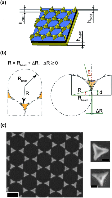 | ||
| Fig. 1 Geometry of the proposed absorber. (a) Schematic representation of the MIM absorber consisting of a gold back reflector, a SiO2 dielectric spacer, and a patterned gold front layer with thicknesses hAuBR, hSiO2, and hAuFP, respectively. (b) Definition of the in-plane geometrical parameters of the front gold pattern: Rbead is the radius of the spherical beads used in the NSL, and R is defined as the radius of curvature of the pattern. ΔR represents the difference between R and Rbead and can be adjusted in the fabrication. 2θ and 2d are the tip tapering angle and the distance between two neighboring tips, respectively. (c) Left: top-view scanning electron micrograph of a fabricated structure. Scale bar is 200 nm. Right: magnified top views of single tapered triangles. Scale bars are 50 nm. | ||
The performance of the proposed absorber is illustrated in Fig. 2b–j, where the measured and calculated absorption spectra are plotted for different values of ΔR. The other geometrical parameters are fixed at Rbead = 150 nm and hSiO2 = 60 nm (see Fig. 2a), and the thickness of the back reflector and the gold triangles are both equal to 100 nm. The overall structure is only 260 nm thick. The numerical simulations are carried out using the COMSOL Multiphysics package (RF Module)‡ and the absorption measurements were performed using a home-built inverted microscope. Collimated white light was used for excitation and the absorption spectrum, A, was calculated as A = (I − R)/I, where I and R are the incident (excitation) and reflected spectra, respectively. The light transmitted through the absorber was negligible.‡
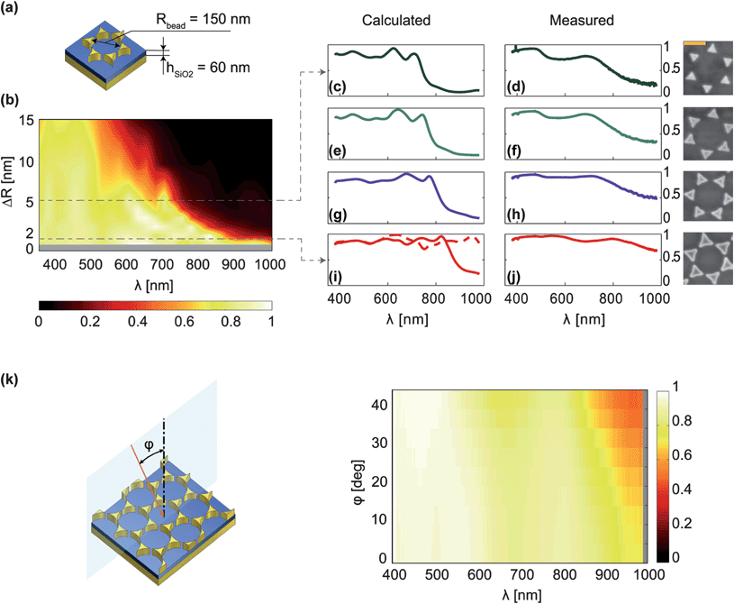 | ||
| Fig. 2 Measured and calculated absorption spectra of the absorbers. (a) Schematic representation of a unit cell of the absorber. In all studied cases Rbead and hSiO2 are kept constant while ΔR is varied. (b) Simulated absorption plotted as a function of wavelength λ and ΔR. The absorption bandwidth is very large for small positive ΔR's. Simulations for ΔR between 0 nm and 1 nm turned out to be very challenging and beyond our capabilities (gray area). (c–j) Calculated (left column) and measured (right column) absorption spectra for different values of ΔR; from top to bottom: ΔR = 6 nm (c and d), 4 nm (e and f), 3 nm (g and h), 2 and 1 nm (i and j). The spectral response for the case of small ΔR becomes very sensitive to slight changes in this value. Therefore, the ultra-broadband absorption behavior observed in (j) can be viewed as the result of a superposition of different cases with slightly different ΔR values, two typical values of which are calculated in (i): solid (ΔR = 2 nm) and dashed (ΔR = 1 nm) lines. The SEM pictures on the right show unit cells of the fabricated structure for each case. Scale bar is 200 nm. (k) Left: schematic drawing of the absorber with light incident at an angle φ. Right: experimentally measured absorption plotted as a function of wavelength λ and angle of incidence φ. The objective used for excitation (NA = 0.75) allowed excitation angles up to φ = 48°. | ||
Both simulation and experimental data suggest that decreasing ΔR (equivalently decreasing 2θ) increases the absorption bandwidth while maintaining reasonably high absorption within the bandwidth. The best experimental result in terms of broadness is obtained at ΔR ≈ 2 nm (see Fig. 2j), for which the neighbouring tapered triangles' tips are at the closest distance but still separated. Here, absorption stays above 85% within the spectral range of 380–850 nm and slowly drops to 70% at 980 nm. We reach an average absorption slightly higher than 88% within the spectral range of 380–980 nm. The numerical results in Fig. 2b show a rapid increase in the absorption bandwidth as ΔR approaches zero (equivalently, the distance between the tips of neighbouring triangles as well as θ decrease). As mentioned above, ΔR can be controlled with nanometer resolution by using a slow enough etching process. While the fabrication relies on a facile method, the results show the potential of the proposed concept to easily adjust the absorption bandwidth and achieve a near-ideal absorber.
Angular insensitivity is one of the important properties of an ideal absorber. To assess the angular sensitivity of our absorber we illuminated it with plane waves at different angles of incidence. We obtained this by focusing the excitation light at different positions on the back-focal plane of the objective with which we were able to reach angles up to 48 degrees (numerical aperture, NA = 0.75). The measured absorption spectra for the best experimental case (Fig. 2j) for incidence angles from 0 to 45 degrees are summarized in Fig. 2k. The results show that a broad absorption spectrum is preserved even at large angles of incidence.26 Finally, our design concept is inherently polarization insensitive at normal incidence. This is due to the geometrical planar symmetries that it contains. In addition, the measurements, which are performed with unpolarized light, and the simulations (not shown for brevity) confirm a similar insensitivity for angles away from the normal.
The broadband absorption behaviour of our design is the collective result of a number of plasmonic absorption events. These events occur at different locations of the spectrum and, after appropriate choice of the geometrical dimensions, piece together a continuous absorption band. To assess the impact of the dielectric spacer thickness, in Fig. 3a we show the calculated absorption spectra for different values of hSiO2. All of the other geometrical parameters are kept constant (Rbead = 150 nm, hAu,FP = 100 nm, ΔR = 2 nm, see Fig. 2a). The horizontal dashed line shows the situation that we have in the experiment, hSiO2 = 60 nm (Fig. 2j), which leads to very high absorption over the entire absorption spectrum. Moving away from this optimal thickness leads to the appearance of spectral bands with high reflection in the visible range. To understand the origin of the broadband absorption, we studied the field distributions inside the dielectric layer on two horizontal cross-sections, close to the top pattern and close to the back reflector. Fig. 3d shows magnetic field enhancement profiles at four absorption peaks indicated by P1–P4 in Fig. 3a.
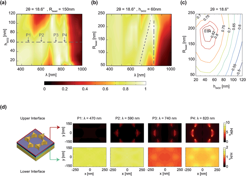 | ||
| Fig. 3 Absorption spectra vs. geometrical parameters and field profiles. (a) Simulated absorption spectrum as a function of hSiO2 for Rbead = 150 nm and hAuBR = hAuFP = 100 nm. The dashed line indicates the best case, which also corresponds to the experimentally realized absorber. The arrows P1–P4 indicate the position of the main absorption peaks. (b) Simulated absorption spectrum as a function of Rbead for hSiO2 = 60 nm and hAuBR = hAuFP = 100 nm. The eye-guiding dotted and dotted-dashed lines show the change in the absorption peaks corresponding to P3 and P4, respectively. (c) Contour plot showing total absorption of sunlight, Atot, as a function of geometrical parameters Rbead and hSiO2. In order to compare similar tip geometries, ΔR/Rbead is kept constant and equal to 0.0133 (2θ = 18.6°). Absorption is calculated within the spectral range of 350–1000 nm assuming the solar irradiance for the standard AM1.5 (air mass) spectrum. (d) Normalized magnetic field (H) profiles at two cross-sections within the SiO2 layer for the cases specified by P1–P4 in (a) (upper cross-section: interface between the front Au pattern and the SiO2 layer; lower cross-section: interface between the SiO2 layer and the gold back reflector). | ||
At P1 (λ = 470 nm) we note that the electromagnetic energy is concentrated close to the back-reflector. This indicates that the absorption at this wavelength originates from the grating-mediated coupling of electromagnetic field to the surface plasmon polariton (SPP) excited at the interface between the SiO2 layer and the gold back reflector.27 Our analytical calculations for the simplified three-layer (air–SiO2–gold) structure predict the grating coupled SPP (corresponding to the grating period = 2Rbead = 300 nm) at λ = 498 nm (see ESI, Fig. S2†), which is close to the observed resonance. This absorption resonance only slightly blue-shifts as the value of hSiO2 increases. The absorption peak at P2 (λ = 590 nm) is substantially influenced by hSiO2 and becomes weaker for SiO2 thicknesses away from 60 nm. This peak red-shifts as hSiO2 increases and is a result of a dipole–dipole interaction between the triangles and the gold back reflector.28 The field profiles in Fig. 3d (P2) verify the contribution of both triangles and the back reflector to this resonance. The absorption event at P3 mainly originates from the localized surface plasmon (LSP) resonance of the individual tapered triangles. Our simulations of an isolated tapered triangle on a glass substrate reveal a dominant absorption peak for λ close to 720 nm (see ESI, Fig. S3†) which complies with the observed resonance at P3. The position of this absorption peak is only slightly influenced by hSiO2 and the weak field enhancement on the back reflector confirms the dominant contribution of the individual triangles to the resonance (see Fig. 3d (P3)). Absorption at P4 originates from the presence of the tips where energy is accumulated and dissipated. This is evident from the strong field enhancement at the tips shown in Fig. 3d (P4).
Further evidence for the above-mentioned attributes is given in Fig. 3b, where calculated absorption spectra are plotted as a function of Rbead. Here, by maintaining the ratio ΔR/Rbead constant, we are able to keep the tip angle, 2θ, constant and equal to 18.6°. Other geometrical values are hSiO2 = 60 nm and hAu,FP = 100 nm. The two eye-guiding lines show the variation of the position of the resonances corresponding to P3 and P4 (see Fig. 3a). The resonance corresponding to P3 (dotted line) red-shifts as Rbead increases. This is in agreement with the expected red-shift of the LSP resonance of the triangles as their size (or equivalently Rbead) increases.29 On the other hand, the invariance of 2θ ensures a practically unchanged spectral position of the absorption peak corresponding to P4 (dashed-dotted line), although Rbead and 2d (see Fig. 1b) vary over a large range. As expected from previous studies,30 the focusing of the electromagnetic energy at the end of tapered tips is sensitive only to the tip opening angle. The spectral position of this absorption peak determines the upper cut-off of the absorption band and as seen in Fig. 2b can be greatly increased by decreasing the tip angle, 2θ.
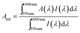
In order to assess the performance of our concept in absorbing the solar spectrum, we calculate the total absorption as
Conclusions
In conclusion, exploiting a combination of different plasmonic absorption phenomena in an array of tapered triangles integrated in an MIM configuration, we introduced a novel ultra-broadband plasmonic absorber with average absorption 88% within the spectral range of 380–980 nm. In addition, this absorber is insensitive to both light polarization and angle of incidence. While aspects of light absorption by arrays of tapered triangles have been studied before, our results contain significant novelty based on exploiting simultaneously four distinct absorption phenomena (each of different nature) two of which are accessible only through the MIM configuration. By suitably selecting a host of geometrical dimensions, we managed to harvest the collective benefit of these absorption events and pieced together a continuous absorption band. Our simulations show that one could go even beyond these high values, in terms of broadness and total absorption, by fine-tuning the geometrical parameters, specifically the tip regions of the tapered triangles in the pattern. Importantly, in contrast to previous successful designs, the fabrication of our concept is based on NSL which is a low-cost and easily accessible method.21,23 Although monocrystallinity is not a stringent requirement in our design, achieving large defect-free crystals with NSL remains a challenge. This bottleneck has been addressed in recent studies31,32 and significant improvements are foreseen. To this end, and based on the nano-scale thickness (260 nm) of our design, we envision the up-scaling of the absorber on flexible substrates even in a roll-to-roll manner. Being ultra-thin, the absorber can efficiently and rapidly elevate the temperature within a nano-scale layer, which can be exploited in various applications such as micro-fluidics,33 solar thermoelectrics4,9,34 and high temperature chemical reactions.35 In addition, efficiently absorbing the extremely broad solar light and concentrating it at the very end of the tips renders the present concept an interesting candidate for enhancing solar-based photochemistry and improving the efficiency of solid-state devices.5–8References
- H. A. Atwater and A. Polman, Nat. Mater., 2010, 9, 205–213 CrossRef CAS PubMed.
- J. V. van de Groep, P. Spinelli and A. Polman, Nano Lett., 2012, 12, 3138–3144 CrossRef CAS PubMed.
- C. H. Wu, B. Neuner, J. John, A. Milder, B. Zollars, S. Savoy and G. Shvets, J. Opt., 2012, 14, 024005 CrossRef.
- Y. J. Xiong, R. Long, D. Liu, X. L. Zhong, C. M. Wang, Z. Y. Li and Y. Xie, Nanoscale, 2012, 4, 4416–4420 RSC.
- S. C. Warren and E. Thimsen, Energy Environ. Sci., 2012, 5, 5133–5146 CAS.
- S. Linic, P. Christopher and D. B. Ingram, Nat. Mater., 2011, 10, 911–921 CrossRef CAS PubMed.
- F. M. Wang and N. A. Melosh, Nano Lett., 2011, 11, 5426–5430 CrossRef CAS PubMed.
- M. W. Knight, H. Sobhani, P. Nordlander and N. J. Halas, Science, 2011, 332, 702–704 CrossRef CAS PubMed.
- D. Kraemer, B. Poudel, H. P. Feng, J. C. Caylor, B. Yu, X. Yan, Y. Ma, X. W. Wang, D. Z. Wang, A. Muto, K. McEnaney, M. Chiesa, Z. F. Ren and G. Chen, Nat. Mater., 2011, 10, 532–538 CrossRef CAS PubMed.
- A. Moreau, C. Ciraci, J. J. Mock, R. T. Hill, Q. Wang, B. J. Wiley, A. Chilkoti and D. R. Smith, Nature, 2012, 492, 86–89 CrossRef CAS PubMed.
- M. K. Hedayati, M. Javaherirahim, B. Mozooni, R. Abdelaziz, A. Tavassolizadeh, V. S. K. Chakravadhanula, V. Zaporojtchenko, T. Strunkus, F. Faupel and M. Elbahri, Adv. Mater., 2011, 23, 5410–5414 CrossRef CAS PubMed.
- M. Elbahri, S. Homaeigohar, R. Abdelaziz, T. Dai, R. Khalil and A. U. Zillohu, Adv. Funct. Mater., 2012, 22, 4771–4777 CrossRef CAS.
- A. De Luca, N. Depalo, E. Fanizza, M. Striccoli, M. L. Curri, M. Infusino, A. R. Rashed, M. La Deda and G. Strangi, Nanoscale, 2013, 5, 6097–6105 RSC.
- K. Aydin, V. E. Ferry, R. M. Briggs and H. A. Atwater, Nat. Commun., 2011, 2, 517 CrossRef PubMed.
- M. G. Nielsen, A. Pors, O. Albrektsen and S. I. Bozhevolnyi, Opt. Express, 2012, 20, 13311–13319 CrossRef.
- A. Aubry, D. Y. Lei, A. I. Fernandez-Dominguez, Y. Sonnefraud, S. A. Maier and J. B. Pendry, Nano Lett., 2010, 10, 2574–2579 CrossRef CAS PubMed.
- J. B. Pendry, A. Aubry, D. R. Smith and S. A. Maier, Science, 2012, 337, 549–552 CrossRef CAS PubMed.
- E. E. Narimanov and A. V. Kildishev, Appl. Phys. Lett., 2009, 95, 041106 CrossRef.
- T. Sondergaard, S. M. Novikov, T. Holmgaard, R. L. Eriksen, J. Beermann, Z. H. Han, K. Pedersen and S. I. Bozhevolnyi, Nat. Commun., 2012, 3, 969 CrossRef PubMed.
- T. Sondergaard and S. I. Bozhevolnyi, New J. Phys., 2013, 15, 013034 CrossRef.
- J. C. Hulteen and R. P. Vanduyne, J. Vac. Sci. Technol., A, 1995, 13, 1553–1558 Search PubMed.
- B. J. Y. Tan, C. H. Sow, T. S. Koh, K. C. Chin, A. T. S. Wee and C. K. Ong, J. Phys. Chem. B, 2005, 109, 11100–11109 CrossRef CAS PubMed.
- X. Y. Zhang, A. V. Whitney, J. Zhao, E. M. Hicks and R. P. Van Duyne, J. Nanosci. Nanotechnol., 2006, 6, 1920–1934 CrossRef CAS PubMed.
- S. R. Ye, A. L. Routzahn and R. L. Carroll, Langmuir, 2011, 27, 13806–13812 CrossRef CAS PubMed.
- E. D. Palik and G. Ghosh, Handbook of optical constants of solids, Academic Press, San Diego, 1998 Search PubMed.
- N. Liu, M. Mesch, T. Weiss, M. Hentschel and H. Giessen, Nano Lett., 2010, 10, 2342–2348 CrossRef CAS PubMed.
- Y. Z. Chu and K. B. Crozier, Opt. Lett., 2009, 34, 244–246 CrossRef CAS.
- W. Rechberger, A. Hohenau, A. Leitner, J. R. Krenn, B. Lamprecht and F. R. Aussenegg, Opt. Commun., 2003, 220, 137–141 CrossRef CAS.
- K. L. Kelly, E. Coronado, L. L. Zhao and G. C. Schatz, J. Phys. Chem. B, 2003, 107, 668–677 CrossRef CAS.
- Y. Luo, J. B. Pendry and A. Aubry, Nano Lett., 2010, 10, 4186–4191 CrossRef CAS PubMed.
- G. D. Moon, T. I. Lee, B. Kim, G. Chae, J. Kim, S. Kim, J. M. Myoung and U. Jeong, ACS Nano, 2011, 5, 8600–8612 CrossRef CAS PubMed.
- C. C. Ho, P. Y. Chen, K. H. Lin, W. T. Juan and W. L. Lee, ACS Appl. Mater. Interfaces, 2011, 3, 204–208 CAS.
- J. S. Donner, G. Baffou, D. McCloskey and R. Quidant, ACS Nano, 2011, 5, 5457–5462 CrossRef CAS PubMed.
- K. Moth-Poulsen, D. Coso, K. Borjesson, N. Vinokurov, S. K. Meier, A. Majumdar, K. P. C. Vollhardt and R. A. Segalman, Energy Environ. Sci., 2012, 5, 8534–8537 CAS.
- C. Fasciani, C. J. B. Alejo, M. Grenier, J. C. Netto-Ferreira and J. C. Scaiano, Org. Lett., 2011, 13, 204–207 CrossRef CAS PubMed.
Footnotes |
| † Electronic supplementary information (ESI) available: Detailed geometry description; set-up description; literature comparison; surface plasmon polariton dispersion curve; absorption efficiency of an isolated tapered triangle on glass. See DOI: 10.1039/c3nr03273f |
‡ Fabrication procedure details. Clean glass coverslips (18 × 18 mm) were coated first with a 100 nm gold back reflector (electron beam evaporation) and successively with a 60 nm SiO2 layer (plasma enhanced chemical vapor deposition). The thickness of the dielectric spacer and optical properties of SiO2 and gold layers were always measured using ellipsometry. After cleaning with a 6![[thin space (1/6-em)]](https://www.rsc.org/images/entities/char_2009.gif) :1:1 solution of H2O:NH4OH:H2O2 in an ultrasonic bath for 10 min, the samples were stored for 24 h in ethanol to ensure full hydrophilicity of the glass surface. The hexagonal gold patterns are fabricated using nanosphere lithography (NSL) and etching techniques. First, a closely packed monolayer of polystyrene beads (Sigma Aldrich, diameter 300 nm) is created using dip-coating (see ESI S2† for the set-up): the sample is quickly immersed into a diluted bead solution (1 wt%, 10−3 M SDS) and then withdrawn with controlled velocity (≈2.5 μm s−1). The humidity is kept constant at ≈50%. Then, reactive ion etching is used to reduce the bead size (100 sccm Ar, 10 sccm O2, 50 W, 100 μbar). The bead size is controlled by adjusting the etching time. Due to overshadowing in the NSL,24 zero or short etching times result in disconnected curved triangles (ΔR > 0). The final pattern is created by evaporating 100 nm of gold (after 2 nm Cr adhesion layer) through the bead mask and by successively removing the beads by low power ultrasonication.Optical Measurements. Absorption measurements are performed using a home-built inverted microscope equipped with an air objective (numerical aperture 0.75) for exciting the sample and collecting the reflected and scattered light and a spectrometer (Princeton Instruments). White light is generated by a xenon lamp and is brought to the set-up with an optical fiber (105 μm core size) in order to improve its spatial coherence. Plane wave excitations with different angles of incidence are achieved by focusing the light beam at different positions on the back focal plane of the objective. The relation A = (I − R)/I was used to calculate the absorption spectrum, where A, I and R are the absorption, incident (excitation) and reflected spectra, respectively. The light transmitted through the absorber was negligible. I was measured using the reflected spectrum from a broadband silver mirror. This ensures accounting for excitation spectral non-uniformity and loss along the detection path. Furthermore, dark counts of the spectrometer and background spectra were subtracted from all the measured spectra.Simulations. Primary estimation of optimal dimensions was achieved by performing a large series of full-wave simulations with Lumerical, a commercially available finite-difference time-domain (FDTD) software package, which is very efficient for broadband simulations. However, due to the staircasing errors of FDTD at sharp edges, the final simulations (which include all the results shown in this manuscript) were performed using the COMSOL Multiphysics package (RF module), which is based on the finite element method (FEM). By using symmetry and periodic (for normal excitation) or Floquet (for oblique excitation) boundary conditions the computational domain was reduced to one-fourth of a unit-cell. To model gold in the simulations, we used the optical properties tabulated in Palik's Handbook25 which agree well with our ellipsometry measurements (see Fabrication procedure details). :1:1 solution of H2O:NH4OH:H2O2 in an ultrasonic bath for 10 min, the samples were stored for 24 h in ethanol to ensure full hydrophilicity of the glass surface. The hexagonal gold patterns are fabricated using nanosphere lithography (NSL) and etching techniques. First, a closely packed monolayer of polystyrene beads (Sigma Aldrich, diameter 300 nm) is created using dip-coating (see ESI S2† for the set-up): the sample is quickly immersed into a diluted bead solution (1 wt%, 10−3 M SDS) and then withdrawn with controlled velocity (≈2.5 μm s−1). The humidity is kept constant at ≈50%. Then, reactive ion etching is used to reduce the bead size (100 sccm Ar, 10 sccm O2, 50 W, 100 μbar). The bead size is controlled by adjusting the etching time. Due to overshadowing in the NSL,24 zero or short etching times result in disconnected curved triangles (ΔR > 0). The final pattern is created by evaporating 100 nm of gold (after 2 nm Cr adhesion layer) through the bead mask and by successively removing the beads by low power ultrasonication.Optical Measurements. Absorption measurements are performed using a home-built inverted microscope equipped with an air objective (numerical aperture 0.75) for exciting the sample and collecting the reflected and scattered light and a spectrometer (Princeton Instruments). White light is generated by a xenon lamp and is brought to the set-up with an optical fiber (105 μm core size) in order to improve its spatial coherence. Plane wave excitations with different angles of incidence are achieved by focusing the light beam at different positions on the back focal plane of the objective. The relation A = (I − R)/I was used to calculate the absorption spectrum, where A, I and R are the absorption, incident (excitation) and reflected spectra, respectively. The light transmitted through the absorber was negligible. I was measured using the reflected spectrum from a broadband silver mirror. This ensures accounting for excitation spectral non-uniformity and loss along the detection path. Furthermore, dark counts of the spectrometer and background spectra were subtracted from all the measured spectra.Simulations. Primary estimation of optimal dimensions was achieved by performing a large series of full-wave simulations with Lumerical, a commercially available finite-difference time-domain (FDTD) software package, which is very efficient for broadband simulations. However, due to the staircasing errors of FDTD at sharp edges, the final simulations (which include all the results shown in this manuscript) were performed using the COMSOL Multiphysics package (RF module), which is based on the finite element method (FEM). By using symmetry and periodic (for normal excitation) or Floquet (for oblique excitation) boundary conditions the computational domain was reduced to one-fourth of a unit-cell. To model gold in the simulations, we used the optical properties tabulated in Palik's Handbook25 which agree well with our ellipsometry measurements (see Fabrication procedure details). |
| This journal is © The Royal Society of Chemistry 2013 |