Templated assembly of Co–Pt nanoparticles via thermal and laser-induced dewetting of bilayer metal films†
Yong-Jun
Oh
*a,
Jung-Hwan
Kim
a,
Carl V.
Thompson
b and
Caroline A.
Ross
*b
aDepartment of Advanced Materials Science and Engineering, Hanbat National University, 125, Dongseo-daero, Yuseong-gu, Daejeon 305-719, Korea. E-mail: yjoh@hanbat.ac.kr
bDepartment of Materials Science and Engineering, Massachusetts Institute of Technology, Cambridge, MA 02139, USA. E-mail: caross@mit.edu
First published on 23rd November 2012
Abstract
Templated dewetting of a Co/Pt metal bilayer film on a topographic substrate was used to assemble arrays of Co–Pt alloy nanoparticles, with highly uniform particle size, shape and notably composition compared to nanoparticles formed on an untemplated substrate. Solid-state and liquid-state dewetting processes, using furnace annealing and laser irradiation respectively, were compared. Liquid state dewetting produced more uniform, conformal nanoparticles but they had a polycrystalline disordered fcc structure and relatively low magnetic coercivity. In contrast, solid state dewetting enabled formation of magnetically hard, ordered L10 Co–Pt single-crystal particles with coercivity >12 kOe. Furnace annealing converted the nanoparticles formed by liquid state dewetting into the L10 phase.
Introduction
Poorly wetting metallic thin films on solid surfaces are unstable to agglomeration at high temperature, which has led to the emergence of “dewetting” techniques for the intentional creation of particles of metal (or other materials) from continuous thin films. Recently, dewetting (or agglomeration) has received renewed attention due to its ability to control the locations and sizes of the nanoparticles if the rupture and agglomeration of the films is templated by substrate features.1–6 Dewetting techniques can potentially be used to synthesize metal particles for a variety of nanotechnology-based applications including patterned magnetic recording media,3,7 plasmon resonance wave guides,8,9 and plasmon-enhanced photovoltaic devices10–13 and as catalysts for nanowire growth.14 Recently, dewetting has been studied in films of several pure metals (Au,4,15,27 Ag,16,17 Ni,14 Co,3,18 or Pt19), alloy systems (Co–Pd,20 Au–Ag,21,22 and Cu–Ni23,24) and immiscible systems (Au–Ni25 and Ag–Co26–29). Templated dewetting has mostly been explored for a single layer of pure metal,3,4,30,31 and templated dewetting in alloys or bilayer metals is not well explored, apart from a recent report for Au–Ag.22 In this work we describe templated dewetting in the Co–Pt bilayer system.Dewetting can occur in two fundamentally different regimes: liquid-state dewetting (LSD) which is governed by hydrodynamic flow of the liquid melted film, and solid-state dewetting (SSD), which generally occurs through capillary-driven diffusion on the surface of the film, which remains solid during the dewetting process. Theories on the dewetting instability in LSD have primarily been based on hydrodynamic considerations2,28,32–34 and refined based on empirical observations of polymer and metallic films dewetted by thermal annealing and pulsed-laser irradiation, respectively.29,35,36 From these considerations, two mechanisms in the dewetting evolution of a metastable liquid film in LSD can be identified:37,38 nucleation and spinodal dewetting. Very thin continuous films sometimes undergo spinodal dewetting, which occurs when attractive dispersion forces between the film's surfaces amplifies thickness fluctuations, leading to a bicontinuous pattern of hills and valleys and eventual film rupturing. In contrast, when films are thick, dewetting can be initiated heterogeneously by the nucleation of holes at surface defects, followed by hole expansion and fragmentation of ligaments to form isolated droplets.
Dewetting solid metallic films by SSD can also proceed through a nucleation-like process in which holes form at locations of crystalline or other defects.3–5 Commonly, polycrystalline solid metallic films are known to dewet through formation of holes at grain boundary triple junctions, followed by retraction of the hole edges through capillary-driven surface diffusion, formation of ligaments due to instabilities of the rims of the retracting edges, and formation of particles due to a Rayleigh-like instability of the ligaments.5,39 In SSD, the phase and orientation of the particles are directly linked to the crystal structure and preferred crystal orientation of the original film. In this respect, we expect that SSD would be the more suitable method for controlling the crystal structure and orientation of dewetted metal particles compared with LSD using a laser.
In either regime, there are currently two main approaches for controlling dewetting and achieving a designed particle pattern on a solid surface: creating regular topography on the substrate on which the film is deposited, or physically constraining the area of the film to a certain geometry by patterning it before dewetting. Periodically patterned topographic substrates impose undulations in an as-deposited film, giving rise to a modulation in the film curvature.3,4 In SSD, this curvature modulation induces atomic diffusion toward the locations with the lowest local excess chemical potential and leads to an ordered dewetting process. For example, Giermann and Thompson dewetted solid Au films on a (100)-silicon template (coated with thin silicon oxide) with ordered inverted pyramidal pits, and showed that the particles developed a <100> crystallographic texture4 attributed to the minimization of the interfacial energy between the as-deposited fcc-Au and all four of the silicon oxide surfaces in the inverted pyramidal pit.
Pre-patterning of films to create to make regular arrays of film edges (e.g. holes or patches) can also be used to direct the dewetting process in LSD or SSD;1,24,40–42 when annealed at high temperature or heated above the melting threshold, a sufficiently narrow thin film strip retracts and breaks up to form a single line of droplets. An artificial perturbation of the strip edge, which is designed to tune the amplitude and period of destabilization, can dramatically enhance the quality of self-assembly during LSD.1 Ye and Thompson dewetted single-crystal Ni films patterned into patches with a variety of shapes via SSD, and showed that the edge retraction velocity during SSD could be controlled by the initial in-plane orientation of the edge.41,42
Arrays of magnetic alloy nanoparticles have received considerable attention for high-density data storage and magneto-optical applications.43 In patterned media systems, where the magnetization direction of each particle represents one bit of information, the storage density is determined directly by the areal density of nanoparticles. Most notably, a great deal of effort has been made to form Co–Pt and Fe–Pt particles in the L10 phase because these alloys have high anisotropy and are therefore magnetically thermally stable even at extremely small sizes (<10 nm), promising increased storage density in patterned media where each particle stores one bit. Particles with such a small size can be achieved via a chemical synthesis.44–46 However, significant challenges remain to be solved to enable the use of these materials, as outlined by Terris and Thomson.43 Typically, the crystal structure of as-synthesized nanoparticles is a disordered fcc phase which has a lower magnetic anisotropy than the ordered phase, and the magnetic easy axes are randomly oriented. Consequently the particles require annealing for conversion into the L10 phase and to control the easy axis direction, which involves a considerable risk of disrupting the particle size distribution.43,47 Templated dewetting techniques may offer solutions for these challenges.
This article reports the assembly of ordered arrays of Co–Pt particles via the dewetting of Co/Pt bilayer films on a topographic template. Two dewetting methods – SSD by furnace annealing and LSD by irradiation with a pulsed-UV laser – were studied, and their influences on the shape, crystal structure and orientation, and collective magnetic properties of the resulting nanoparticle arrays are compared. Since dewetting of bilayer films involves chemical mixing concurrently with the film agglomeration, bilayer systems are expected to show an interesting range of contrasting behavior during SSD and LSD.
Results and discussion
The Co–Pt compositions of the alloys used in this study were 48%Co–52%Pt (CP52) and 64%Co–36%Pt (CP36) in atomic%, which are located within the ordered L10 face centered tetragonal (fct) and the disordered face centered cubic (fcc) phase regions of the Co–Pt phase diagram at room temperature, respectively. The order–disorder phase transition temperature in bulk Co–50 at.%Pt alloy is 825 °C. The targeted chemical compositions of the alloy nanoparticles were obtained by adjusting the layer thickness ratios in the deposited bilayer films. The total thickness of the Co/Pt bilayer film was 12 nm and the chemical composition of CP52 was obtained from the films with a Pt to Co thickness ratio of 4.5 nm/7.5 nm.Fig. 1 shows the morphology of Co–Pt samples formed by SSD furnace-annealing at 800 and 900 °C on both smooth substrates and on substrates patterned with inverted pyramids. The metal particles are clearly defined and assembled into the inverted pyramidal pits of Fig. 1(a) and (b) with only a small amount of metal remaining on the mesas that separate the pits. In Fig. 1(e) the perforated nitride layer used as an etch mask to make the inverted pyramids was not removed prior to metal deposition and annealing. This template created an array of particles with diameters of 45 nm (Fig. 1(e)) inside the pits that formed below the perforations in the nitride. Additional particles of poorer uniformity were located on the widest parts of the nitride mesas. The distributions of the chemical compositions and sizes of the particles are shown in Fig. 1(d) and (f), respectively. For comparison, particles dewetted on a smooth silica substrate are shown in Fig. 1(c).
 | ||
| Fig. 1 SEM images of Co–52 at.%Pt particles formed by annealing at (a) 800 °C for 5 h, or (b), (c) and (e) 900 °C for 2 h. Image (c) was obtained using a smooth silica substrate, and image (e) used a template with a perforated silicon nitride top-layer that was undercut by inverted pyramids etched into the underlying silicon. (d) The distribution of Pt content in the particles from samples shown in (b) and (c). (f) Size distribution of the particles in images (a), (b), (c) or (e). The size distribution for image (e) was obtained only for the particles in the pits. | ||
The particles formed by SSD on the topographic template exhibited an excellent uniformity in both chemical composition and size compared to those formed on the smooth template. Based on the compositional variation of NPs formed on the smooth substrate, we postulate that the metal bilayers were not significantly intermixed before they ruptured and fragmented to form nanoparticles. As noted previously, metallurgical defects such as grain boundaries initiate a SSD process in relatively thick metallic films. If this occurred in different locations for the Co and Pt layers it would lead to particles with different average compositions. However, on the template with inverted pyramidal pits, the two metal films are assumed to have ruptured preferentially at the narrow mesas between the pits, leading to much less variation in chemical composition and particle volume.
The crystal structure and orientation of the agglomerated nanoparticles were investigated by collecting plane-view and cross-sectional TEM images. Fig. 2 illustrates in plane view the CP52 and CP36 NPs formed via SSD at 900 °C in the inverted pyramids. Twin boundaries are visible, but the particles are mainly single crystals, as shown in the selected area diffraction (SAD) pattern. The crystal structure was identified as ordered fct L10 for CP52 with strong superlattice reflections in the diffraction pattern and disordered fcc for CP36, as predicted from the equilibrium phase diagram. In addition to the particles in the apices, tiny particles with sizes of a few nanometers were scattered on the silica as shown in Fig. 2(a). TEM pattern analysis of those particles revealed that they were a mixture of ordered fct and disordered fcc Co–Pt phases, despite having formed from the CP52 film. This result could be caused by suppression of the ordering reaction that occurs in such small particles. Alloyeau et al. showed that for 3 nm Co–Pt particles the transition temperature could be reduced by at least 175 °C.48 A lowered ordering temperature would promote formation of the disordered phase during the furnace annealing step.
 | ||
| Fig. 2 TEM images of (a) Co–52 at.%Pt and (b) Co–36 at.%Pt particles formed by annealing at 900 °C for 2 h. | ||
Fig. 3 shows a typical high-resolution TEM image and diffraction pattern obtained at the [001] and [110] zone axis of CP52 particles formed by SSD. The high-resolution image at the edge of the particle showed a disordered fcc crystalline region with a thickness of 3–4 nanometers, suggesting that the ordering reaction was suppressed at the particle surface. In spite of this, the CP52 particles mostly displayed faceted surfaces. A crystallographic analysis revealed that the facets preferentially consisted of (111), (220) and (200) low-index planes (Fig. 3(b)).
 | ||
| Fig. 3 High-resolution TEM images along the edges of Co–52 at.%Pt particles formed by annealing at 900 °C for 2 h. The majority of particles were transformed into fct crystals, but the surface regions retained the fcc crystal structure. The indices in (b) indicate the side surface planes. | ||
The preferred crystal orientation was determined by obtaining diffraction patterns for individual CP52 particles after SSD. For magnetic recording applications, it is desirable for the magnetic easy axis [001] of the L10 phase to be oriented perpendicular to the substrate plane. To simplify the analysis, we counted the number of particles with low-index zone axes oriented perpendicular to the substrate within a tolerance angle of 10°. This analysis was conducted for 30 particles in each sample to yield statistically significant results. Additional data is given in the ESI.† For the majority of the observed particles, one of the zone axes along the [110], [001] and [112] directions was oriented normal to the substrate, and less than 10% of the observed particles were oriented in other directions. The proportions of each of the three major crystal orientations are plotted against the annealing temperature in Fig. 4. After annealing at 800 °C, the [110] and [112] orientations prevailed, but increasing the annealing temperature increased the prevalence of [110] and reduced the prevalence of [112]. The highest frequency of the [001] texture was obtained for annealing at 900 °C. However, the [001] intensity was weak compared with that of Au particles formed using the same type of topographic silicon template.4
 | ||
| Fig. 4 Relative amount of various crystal orientations of Co–52 at.%Pt particles oriented normal to the silica substrate within a tolerance angle of 10° for particles prepared at different annealing temperatures. | ||
For metallic films with a cubic structure, a perfect [001] texture can be achieved when the {111} facets of the dewetted particle are parallel to the side surfaces of the inverted pyramidal pits in the silicon template.2 However, as observed in Fig. 4, the CP52 particles formed by SSD developed {220} and {200} facets as well as {111}. The Co–Pt fct-L10 structure has a and c-axes of 3.803 and 3.684 Å, respectively, so the {111} facets make a different angle compared to that in a cubic structure (68.82° for fct and 70.53° for cubic) and cannot fit into the inverted pyramidal pits on silicon substrate without undergoing strain. This presumably reduced the frequency of the [001] orientation.
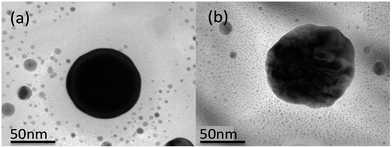
NP arrays were also created by LSD via pulsed-laser irradiation of metal films. Unlike the SSD process, LSD necessarily requires a stacking sequence of Pt bottom (higher melting point) and Co top layers on the substrate to avoid delamination of metal films due to the difference in melting point. Fig. 5 shows the appearance of the CP52 film after 100 pulses at 85 mJ cm−2. The shape of the agglomerated particles conformed to the inverted pyramidal pits in the template (see ESI†), there were fewer particles on the mesas, and, as shown in the bottom in Fig. 5, the size uniformity was further improved compared with the Co–Pt particles formed by SSD in Fig. 1(a) and (b). As previously simulated for Co by Trice et al.,35 the metal film melts for a few nanoseconds and cools to room temperature in ∼1 ms when irradiated by a laser pulse with an energy above the melt threshold. The liquid film contains no metallurgical defects such as grain boundaries, and the partition of the film on the template is thus entirely determined by the template topography, with the film splitting along the tops of the mesas, where the local excess chemical potential is the highest due to film curvature, and forming an array of particles of uniform volume, one within each inverted pyramid.
 | ||
| Fig. 5 SEM image of Co–52 at.%Pt particles after irradiation with 100 pulses of a UV laser at 85 mJ cm−2. The bottom-left is a TEM plan-view image of a particle and the graph is the size distribution of the particles in SEM image. | ||
Fig. 5 inset illustrates the TEM microstructure of a pyramidal particle formed by LSD via laser irradiation. The microstructure is polycrystalline with an fcc structure, showing lattice distortion and crystallographic defects, indicating that the rapid cooling from melt suppressed the formation of the L10 phase and instead retained the high-temperature fcc phase. More detailed TEM data is given in the ESI.†
Fig. 6 shows the microstructure of CP52 particles irradiated by a pulsed laser, followed by furnace annealing at 950 or 700 °C for 2 h. The particle shape was changed from pyramidal after laser irradiation to equiaxed after furnace annealing. Annealing at 950 °C produced particles with a single crystal fct phase, Fig. 6(a), whereas annealing at 700 °C, which is below the order–disorder transition temperature, did not cause the defective polycrystalline structure to coarsen into a single crystal, and the particle showed contrast due to strain, Fig. 6(b). The particles produced by two-step annealing did not exhibit a preferred crystal orientation regardless of whether they were single crystal or not. The highly defective strained structure of the particles obtained using LSD may inhibit the development of preferred orientation in the pits during subsequent annealing.
 | ||
| Fig. 6 TEM image of Co–52 at.%Pt particles irradiated by a pulsed laser followed by furnace annealing at (a) 950 °C or (b) 700 °C for 2 h. | ||
Magnetic properties of the particle arrays formed by SSD were analyzed using a SQUID magnetometer measurement shown in Fig. 7. The CP36 particle array was magnetically soft with very small in-plane and out-of-plane coercivities, corresponding to the disordered fcc Co–Pt phase. However, the coercivity and remanence of the CP52 particles were dramatically increased in both in-plane and out-of-plane measurements. Upon annealing at 800 °C, the array was magnetically isotropic with coercivity of ∼12 kOe. This is consistent with single-domain L10 Co–Pt particles with strong magnetocrystalline anisotropy49,50 but with a distribution of easy axes. Annealing at 900 °C led to an out-of-plane coercivity of 14 kOe and an in-plane value of 10 kOe, as shown in Fig. 7(c). This finding is consistent with the fact that annealing at 900 °C yielded the strongest (001) texture, which enables the easy axis (c-axis) of the ordered Co–Pt crystal to be out of plane. The saturation magnetization Ms was ∼500 emu cm−3 which is lower than the bulk value of ∼800 emu cm−3. The reason for this lower value is not clear but post-annealing oxidation or disorder at the surfaces may contribute. Liou et al. reported Ms = 668 and 586 emu cm−3 for 5 nm thick Co–Pt films annealed at 700 °C for 3 and 12 hours respectively, remarking that the variation may be due to the order and disorder of the Co–Pt phase.51 The samples annealed at 800 and 900 °C show a low-field shoulder in the hysteresis loop. This possibly originates from the small particles of Co–Pt. Disordered fcc Co–Pt or even Co–Pt nanoparticles transformed to the L10 phase can be superparamagnetic due to their small size.
 | ||
| Fig. 7 Magnetic hysteresis loops from Co–36 at%Pt (a) and Co–52 at.%Pt particle arrays (b–d) formed by annealing at (a and c) 900 and (b) 800 °C, and (d) 100 pulses of a UV laser irradiation. | ||
In contrast, Fig. 7(d) shows the M–H loops for the CP52 particles formed by LSD via laser irradiation. The loops show coercivity below 1 kOe and were easier to saturate in plane, similar to the CP36 particles. This behavior is consistent with the rapidly quenched microstructure which retained the high-temperature disordered phase and contained nanocrystalline material. Particles on a smooth substrate showed a similar loop shape and saturation magnetization (see ESI†).
Conclusion
In summary, this study demonstrated that thin-film dewetting using a topographic substrate can be successfully used to assemble alloy nanoparticle arrays from metal bilayers in a similar manner to the assembly of nanoparticle arrays of pure metals. Templated dewetting was striking for producing not just a more uniform size and shape distribution compared to untemplated dewetting, but producing a more uniform composition as a result of the individual Co and Pt layers rupturing at the same locations along the edges of the topography. The comparative dewetting studies showed that solid-state dewetting via furnace annealing was more suitable than liquid-state dewetting via laser irradiation for producing magnetically hard, single-crystal particles with L10 structure and with a temperature-dependent preferred orientation. However, liquid-state dewetting produced alloy particles with greater conformity to the topography and a more uniform size. Appropriate combinations of dewetting and furnace annealing processes applied to multilayer films will enhance the application of ordered alloy nanoparticle assemblies to many functional devices that utilize the magnetic, optoelectrical, and plasmonic properties of metal alloy nanoparticles.Experimental section
Topographic templates consisting of 200 nm period square arrays of inverted pyramidal pits on silicon wafers were prepared from (100) silicon wafers coated with a 40 nm thick silicon nitride layer. Interference lithography with a 325 nm wavelength laser was used to pattern a negative resist to form a square array of holes. The holes in the photoresist were transferred to the silicon nitride layer by wet etching in a concentrated HF solution. A periodic array of pits was formed by anisotropic etching through the nitride holes using a KOH solution. Remaining nitride was removed in HF solution and annealed at 800 °C for 1.5 h to grow 12 nm thick silicon oxide. Other samples were not etched so the nitride was retained, forming a mesa with circular holes undercut by the inverted pyramids. The details of this procedure are described elsewhere.3 Metallic bilayer films were deposited on the templates by RF magnetron sputtering. The films were then annealed in forming gas (Ar + 4%H2), typically for 1–5 h, to induce solid-state dewetting. Liquid-state dewetting was performed using an Nd-YAG laser with a wavelength of 266 nm, a frequency of 10 Hz and a pulse time of 4 ns. Samples were laser annealed for 100 pulses in an atmosphere of Ar + 4%H2 flowing at 50 sccm and several samples were then further annealed at 900 or 700 °C for 2 h in forming gas. The input energy density was determined as the value sufficient to induce complete dewetting at 100 pulses, which was 85 mJ cm−2 for 12 nm thick Co/Pt bilayer films. TEM samples were prepared by wafer back-grinding and ion milling, and cross-sectional samples were cut by a focused ion beam. Composition was measured in TEM using energy dispersive X-ray spectroscopy (EDS). To ensure accuracy, the specimen tilting angle in the TEM was fixed for all EDS measurements, a reference Co–Pt sample was used for calibration before all EDS measurements on nanoparticles, and chemical analysis was conducted with the beam probe focused at the center of the particle. The compositional deviation was below 1.2 at.%Pt when the same Co–Pt particle was repeatedly measured. Magnetic measurements were performed with superconducting quantum interference device (SQUID) magnetometry.Acknowledgements
We thank Profs. H. I. Smith and K. Berggren for interference lithography facilities. This work was partly supported by the Singapore-MIT Alliance and the National Research Foundation of Korea (NRF) grant funded by the Korea government (MEST) (no. 2010-0010001).References and Notes
- J. D. Fowlkes, L. Kondic, J. Diez, Y. Wu and P. D. Rack, Nano Lett., 2011, 11, 2478 CrossRef CAS.
- J. Becker, G. Grun, R. Seemann, H. Mantz, K. Jacobs, K. R. Mecke and R. Blossey, Nat. Mater., 2003, 2, 59 CrossRef CAS.
- Y. J. Oh, C. A. Ross, Y. S. Jung, Y. Wang and C. V. Thompson, Small, 2009, 5, 860 CrossRef CAS.
- A. L. Giermann and C. V. Thompson, Appl. Phys. Lett., 2005, 86, 121903 CrossRef.
- D. Kim, A. L. Giermann and C. V. Thompson, Appl. Phys. Lett., 2009, 95, 251903 CrossRef.
- C. V. Thompson, Annu. Rev. Mater. Res., 2012, 42, 399 CrossRef CAS.
- C. A. Ross, Annu. Rev. Mater. Res., 2001, 31, 203 CrossRef CAS.
- S. A. Maier, P. G. Kik and H. A. Atwater, Phys. Rev. B: Condens. Matter Mater. Phys., 2003, 67, 205402 CrossRef.
- A. Femius Koenderink, Nano Lett., 2009, 9, 4228 CrossRef.
- E. Moulin, J. Sukmanowski, P. Luo, R. Carius, F. X. Royer and H. Stiebig, J. Non-Cryst. Solids, 2008, 354, 2488 CrossRef CAS.
- K. R. Catchpole and S. Pillai, J. Lumin., 2006, 121, 315 CrossRef CAS.
- Yu. A. Akimov, K. Ostrikov and E. P. Li, Plasmonics, 2009, 4, 107 CrossRef CAS.
- T. L. Temple, G. D. K. Mahanama, H. S. Reehal and D. M. Bagnall, Sol. Energy Mater. Sol. Cells, 2009, 93, 1978 CrossRef CAS.
- Y. F. Guan, R. C. Pearce, A. V. Melechko, D. K. Hensley, M. L. Simpson and P. D. Rack, Nanotechnology, 2008, 19, 235604 CrossRef CAS.
- F. Silly and M. R. Castell, Phys. Rev. Lett., 2006, 96, 086104 CrossRef.
- H. Krishna, R. Sachan, J. Strader, C. Favazza, M. Khenner and R. Kalyanaraman, Nanotechnology, 2010, 21, 155601 CrossRef CAS.
- K. Thürmer, E. D. Williams and J. E. Reutt-Robey, Phys. Rev. B: Condens. Matter Mater. Phys., 2003, 68, 155423 CrossRef.
- C. Favazza, J. Trice, H. Krishna and R. Kalyanaraman, Appl. Phys. Lett., 2006, 88, 153118 CrossRef.
- X. Hu, D. G. Cahill, R. S. Averback and R. C. Birtcher, J. Appl. Phys., 2003, 93, 165 CrossRef CAS.
- R. Esterina, X. M. Liu, C. A. Ross, A. O. Adeyeye and W. K. Choi, J. Appl. Phys., 2012, 112, 024312 CrossRef.
- D. Wang and P. Schaaf, J. Mater. Chem., 2012, 22, 5344 RSC.
- D. Wang, R. Ji, A. Albrecht and P. Schaaf, Beilstein J. Nanotechnol., 2012, 3, 651 CrossRef.
- Y. Wu, J. D. Fowlkes and P. D. Rack, J. Mater. Res., 2011, 26, 277 CrossRef CAS.
- J. D. Fowlkes, Y. Wu and P. D. Rack, ACS Appl. Mater. Interfaces, 2010, 2, 2153 CAS.
- D. Wang and P. Schaaf, Mater. Lett., 2012, 70, 30 CrossRef CAS.
- R. Sachan, S. Yadavali, N. Shirato, H. Krishna, V. Ramos, G. Duscher, S. J. Pennycook, A. K. Gangopadhyay, H. Garcia and R. Kalyanaraman, Nanotechnology, 2012, 23, 275604 CrossRef CAS.
- H. Krishna, N. Shirato, S. Yadavali, R. Sachan, J. Strader and R. Kalyanaraman, ACS Nano, 2011, 5, 470 CrossRef CAS.
- M. Khenner, S. Yadavali and R. Kalyanaraman, Phys. Fluids, 2011, 23, 122105 CrossRef.
- S. Yadavali, H. Krishna and R. Kalyanaraman, Phys. Rev. B: Condens. Matter, 2012, 85, 235446 CrossRef.
- D. Wang and P. Schaaf, J. Mater. Sci.: Mater. Electron., 2011, 22, 1067 CrossRef CAS.
- W. K. Choi, T. H. Liew, H. G. Chew, F. Zheng, C. V. Thompson, Y. Wang, M. H. Hong, X. D. Wang, L. Li and J. Yun, Small, 2008, 4, 330 CrossRef CAS.
- A. Sharma and R. Khanna, Phys. Rev. Lett., 1998, 81, 3463 CrossRef CAS.
- S. P. Singh, Adv. Condens. Matter Phys., 2011, 2011, 526397 Search PubMed.
- A. Oron, S. H. Davis and S. G. Bankoff, Rev. Mod. Phys., 1997, 69, 931 CrossRef CAS.
- J. Trice, C. Favazza, D. Thomas, H. Garcia, R. Kalyanaraman and R. Sureshkumar, Phys. Rev. Lett., 2008, 101, 017802 CrossRef.
- R. Xie, A. Karim, J. F. Douglas, C. C. Han and R. A. Weiss, Phys. Rev. Lett., 1998, 81, 1251 CrossRef CAS.
- F. B. Wyart and J. D. Can, J. Phys., 1990, 68, 1084 CAS.
- J. Bischof, D. Scherer, S. Herminghaus and P. Leiderer, Phys. Rev. Lett., 1996, 77, 1536 CrossRef CAS.
- R. Saxena, M. J. Frederick, G. Ramanath, W. N. Gill and J. L. Plawsky, Phys. Rev. B: Condens. Matter Mater. Phys., 2005, 72, 115425 CrossRef.
- J. Ye and C. V. Thompson, Acta Mater., 2011, 59, 582 CrossRef CAS.
- J. Ye and C. V. Thompson, Phys. Rev. B: Condens. Matter Mater. Phys., 2010, 82, 193408 CrossRef.
- J. Ye and C. V. Thompson, Adv. Mater., 2011, 23, 1567 CrossRef CAS.
- B. D. Terris and T. Thomson, J. Phys. D: Appl. Phys., 2005, 38, R199 CrossRef CAS.
- S. H. Sun, C. B. Murray, D. Weller, L. Folks and A. Moser, Science, 2000, 287, 1989 CrossRef CAS.
- T. Hyeon, Chem. Commun., 2003, 927 RSC.
- S. Sun, Adv. Mater., 2006, 18, 393 CrossRef CAS.
- H. Zeng, S. H. Sun, R. L. Sandstrom and C. B. Murray, J. Magn. Magn. Mater., 2003, 266, 227 CrossRef CAS.
- D. Alloyeau, C. Ricolleau, C. Mottet, T. Oikawa, C. Langlois, Y. Le Bouar, N. Braidy and A. Loiseau, Nat. Mater., 2009, 8, 940 CrossRef CAS.
- K. Sato, B. Bian, T. Hanada and Y. Hirotsu, Scr. Mater., 2001, 44, 1389 CrossRef CAS.
- S. Stavroyiannis, I. Panagiotopoulos, D. Niarchos, J. A. Christodoulides, Y. Zhang and G. C. Hadjipanayis, Appl. Phys. Lett., 1998, 73, 3453 CrossRef CAS.
- S. H. Liou, S. Huang, E. Klimek and R. D. Kirby, J. Appl. Phys., 1999, 85, 4334 CrossRef CAS.
Footnote |
| † Electronic supplementary information (ESI) available. See DOI: 10.1039/c2nr32932h |
| This journal is © The Royal Society of Chemistry 2013 |