Large physisorption strain and edge modification of Pd on monolayer graphene
Haiqing
Zhou†
ad,
Fang
Yu†
abd,
Dongsheng
Tang
*c,
Minjiang
Chen
ad,
Huaichao
Yang
ad,
Gang
Wang
ad,
Yanjun
Guo
a and
Lianfeng
Sun
*a
aNational Centre for Nanoscience and Technology, Beijing 100190, China. E-mail: slf@nanoctr.cn; Fax: +86-10-62656765; Tel: +86-10-82545584
bAcademy for Advanced Interdisciplinary Studies, Peking University, Beijing 100871, China
cCollege of Physics and Information Science, Hunan Normal University, Changsha 410081, China. E-mail: dstang@hunnu.edu.cn; Tel: +86-731-88873055
dGraduate School of Chinese Academy of Sciences, Beijing 100049, China
First published on 25th October 2012
Abstract
Using Raman spectroscopic studies, we firstly report that Pd film deposition can induce a tensile strain at the interface between Pd and n-layer graphenes, which results in the splitting of the G peak and a red Raman shift of the 2D peak in monolayer graphene, and red Raman shifts of G and 2D peaks for other n-layer graphenes. In particular, this kind of tensile strain can be used as an effective way for edge modification or strain engineering in monolayer graphene.
Graphene, a single-layer graphite sheet, has attracted increasing attention because of its potential applications in “beyond-silicon” electronics.1–3 In order to investigate the electrical transports through a graphene sheet, making it contact with metal electrodes is necessary.4 Especially, a high-quality metal–graphene junction is very essential for high-performance field effect transistors (FETs) with high carrier mobility, since the metal–graphene contact resistance always exists and depends on the kind of metal electrodes used in the FETs. Recently, due to its importance in graphene-based FETs, both four-probe5–7 and transfer length7,8 measurements have been introduced to investigate the contact resistance. What's more, both first-principles calculations4,9 and electrical transport measurements of graphene devices8 strongly support that the palladium (Pd)–graphene junction is very distinguished compared with other metal species. Even so, it is still an open question to explain the dependence of the metal–graphene contact resistance on contact area, temperature, applied gate potential and the number of graphene layers. In this sense, experimental verification of the interactions among metal and n-layer graphenes is still necessary to give full insight into the physical origin at the metal–graphene interfaces.
In complementary metal oxide semiconductor (CMOS) devices, making use of strain-induced effects is regarded as one of the promising approaches to enhance the carrier mobility of silicon and keep its good electrical performance.10–12 For example, due to the existence of lattice mismatch-induced strain at the interface of SiGe source or drain electrodes, the hole mobility of p-doped silicon devices is greatly boosted. Correspondingly, for graphene, strain also has a profound influence on modulating the electronic structures13–15 and growth of graphene on transition metal surfaces,16,17 or the catalytic activities of metal nanoclusters supported by graphene.18,19 At present, tensile or biaxial strains can be introduced in experiments by designing the supported substrate roughness or transferring graphene samples onto transparent flexible substrates. There are several drawbacks in these two techniques. For the first one, reactive ion etching is usually selected to pattern silicon substrates prior to graphene exfoliation, which is low throughput and expensive. On the other hand, if graphene samples are transferred onto plastic substrates, a tensile strain can be accurately controlled by stretching the flexible substrate in one direction, but the optical contrast of n-layer graphenes on these substrates is very poor compared with that of n-layer graphenes on Si substrates with a 300 nm SiO2 layer. Thus, the poor contrast makes it very difficult to find monolayer graphene by an optical microscope.
Motivated by the above mentioned experiments8 and theoretical calculations,4,9 the objective of the present work is to address whether it is possible to induce a tensile strain in graphene just by depositing metal films onto two sides of graphene as source and drain electrodes, since the mismatch between the lattices of n-layer graphene and metal always exists. Another critical question is how can we detect this kind of tensile strain in cases where metal atoms are thermally deposited onto n-layer graphenes. In this work, we report that due to the lattice mismatch between graphene and Pd, thermal evaporation of a Pd film onto n-layer graphenes can be used as an alternative technique to induce a tensile strain at the interface between n-layer graphene and Pd, which can be efficiently detected using Raman spectroscopy. In particular, this strain has the tendency to modify graphene edges with a larger one due to the stronger interactions of carbon atoms with Pd atoms at graphene edges than that on the graphene surface.
The n-layer graphenes studied in this work were obtained by micromechanical cleavage of natural graphite (Alfa Aesar), and then transferred onto silicon substrates with a 300 nm SiO2 layer.20 Subsequently, optical microscopy (Leica DM4000) and Micro-Raman spectroscopy (Renishaw inVia Raman Spectroscope) were applied to identify the number of graphene layers definitely. To investigate the tensile strain of Pd on graphene, a Pd film was thermally deposited onto graphene samples in a vacuum thermal evaporator at a deposition rate of 1.0 Å s−1 under a vacuum of 10−4 Pa. The film thickness can be well controlled in the range 0.4–1.6 nm by a film thickness monitor (FTM-V). The Pd morphologies on graphenes were characterized by scanning electron microscopy (SEM). As shown in Fig. 1, the morphologies of a Pd film on graphenes are greatly related to the number of graphene layers. With the increase of graphene thickness, single Pd grain size becomes larger, and the Pd film becomes rougher, suggesting thickness-dependent morphologies of Pd on graphenes, which are well consistent with the situation of gold on graphenes.20,21 These phenomena can be attributed to different surface properties of n-layer graphenes or surface diffusion barriers of Pd on n-layer graphenes. Even so, it is quite interesting for us to note that Pd film morphologies are distinctly different on the central and edge regions of n-layer graphenes. Namely, the deposited Pd grains tend to nucleate and grow (or aggregate) at the edges of n-layer graphenes, resulting in the formation of Pd nanowires at the edges of n-layer graphenes, which can be attributed to the short-ranged chemical forces.22 Consequently, it is reasonable for us to suspect that there may be some properties of graphene edges that are different from its surface.
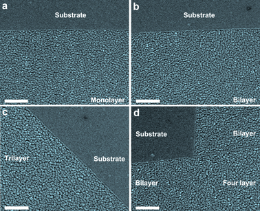 | ||
| Fig. 1 Thickness-dependent morphologies of a 1.6 nm Pd film on n-layer graphenes. Scale bar: 200 nm. (a) Pd film on substrate (top) and monolayer graphene (down). (b) Pd film on substrate (top) and bilayer graphene (down). (c) Pd film on trilayer graphene (left) and substrate (right). (d) Pd film on substrate (top left), bilayer (top and down left) and four layer (right) graphene. It is obviously observable that Pd film morphologies on n-layer graphenes exhibit thickness-dependent behaviors. | ||
As is mentioned above, experimental measurements on the contact resistance of a graphene–Pd junction show an anomalous temperature dependence,8 and a tensile strain is induced in the graphene–Pd junction predicted by theoretical calculations.9
One of the important issues here is how to detect this kind of tensile strain at the interface between graphene and Pd from an experimental point of view. As far as we are concerned, Raman spectroscopy has been proven to be an alternative, efficient and nondestructive technique to attain this goal, since Raman scattering of few-layer graphene is very sensitive to artificial tensile strains.13–15,23–25 For example, when a tensile strain around 0.5% is applied in monolayer graphene, the 2D peak frequency shows red Raman shifts, and the G peak splits into two components (G+ and G− sub-bands).13–15
To identify the presence of a tensile strain in graphene induced by Pd film deposition, we have performed systematic Raman spectroscopic studies to investigate Raman shifts of G and 2D peaks in few-layer graphene, especially G peak splitting for monolayer graphene. The Raman measurements were carried out under ambient conditions with 633 nm (1.96 eV) laser excitation. To avoid laser-induced heating,26,27 we have set the laser power to be below 1.0 mW. Several Raman spectra of pristine or Pd-decorated n-layer graphenes were collected to ensure the repeatability of the results.
The corresponding Raman spectra of Pd film-deposited n-layer graphenes are shown in Fig. 2 and 3. We can find that, compared with other n-layer graphenes and graphite, the G peak of monolayer graphene has split into two distinct G+ (∼1580.3 cm−1) and G− (∼1568.5 cm−1) sub-bands because of the symmetry breaking induced by the strain (Fig. 2a). This means that monolayer graphene is especially vulnerable or sensitive to the Pd deposition-induced tensile strain, which results in the red Raman shifts of the 2D peak (Fig. 3a) and splitting of the G peak (Fig. 2). The elongation of the C–C bonds is commonly accepted as the reason for the red shifts of the 2D band. Since the laser power is always unchanged, and no defect-related Raman peaks are detected during Raman measurements, the G peak splitting and red Raman shifts of the 2D peak can be attributed to the tensile strain induced by Pd deposition, rather than the effects of local heating,26,27 electron-beam radiation28,29 and substrate influence on the Raman spectra of graphene.30,31 Meanwhile, no obvious G peak splitting has been observed on Pd-deposited trilayer, four layer and five layer graphene or graphite. This may be due to the fact that the interaction between graphene and Pd is directly short-ranged with a limited distance level below 1 nm,32 so the tensile strain is very difficult to transfer to thicker graphene samples.13 Furthermore, as shown in Fig. 1, Pd atoms tend to aggregate at the edges of n-layer graphenes, indicating the stronger interaction of Pd atoms with carbon atoms at graphene edges than with the central regions of graphene. Thus, investigating their relevant Raman features may be very interesting, since the electronic properties of graphene would be largely governed by its edge structure.33,34 To reveal the strain effects on graphene edges, we have also performed Raman measurements, which are shown in Fig. 2b. The G peak of monolayer graphene also has split into two components (G+, G−), which is very similar to that collected on the graphene surface. The prominent Raman feature at graphene edges is that the difference values (ΔωG = ωG+ − ωG−, up to 15.1 cm−1) between G+ and G− sub-bands are much larger than those on central regions (∼11.5 cm−1), suggesting that Pd deposition results in a larger tensile strain at graphene edges, which will be discussed below. In sharp contrast, these larger difference values at graphene edges than central regions haven't yet been observed and reported experimentally.14 Therefore, this technique via metal deposition possesses the advantage of detecting the different effects of tensile strains on graphene edge and central regions, and stronger interactions of Pd with carbon atoms at graphene edges than on the graphene surface.
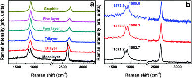 | ||
| Fig. 2 Raman spectra of 1.6 nm Pd-decorated n-layer graphenes (a), and the comparison of Raman spectra collected at the central (black-marked) and edge (red or blue-marked) regions of monolayer graphene after 1.6 nm Pd film deposition. These spectra were excited by 633 nm laser excitation. Compared with other n-layer graphenes, monolayer graphene seems to be much more susceptible to the tensile strain induced by Pd deposition. | ||
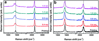 | ||
| Fig. 3 Pd film thickness-dependent physisorption strain effects on Raman spectra of monolayer (a) and bilayer graphene with Pd film thickness from 0.4–1.6 nm. | ||
According to theoretical calculations,9 the film thickness has a serious impact on the average distance of the Pd and graphene layer at the interface. To check this important effect, we have thermally deposited more metal layers on the surface of n-layer graphenes with film thickness ranging from 0.4 nm (∼1 metal monolayer (ML)) to 1.6 nm (∼5 ML). Using a Raman spectroscopy-based technique, the following Raman features can be found for monolayer graphene, as shown in Fig. 3. For one thing, the G peak splits into two components (G+, G−) after 1–5 ML Pd film deposition, indicating the credibility and repeatability of the experimental results reported here. In particular, when the thickness increases to 0.8 nm (around 2 ML), G peak splitting becomes much more distinct, and the 2D peak shows a larger red shift than that for 1 ML Pd on graphene (Fig. 4). For another thing, when more metal layers than 2 ML are deposited onto the graphene surface, obvious G peak splitting is still observable, but the difference values (ΔωG) between the G+ and G− sub-bands and the 2D peak frequency shifts are almost the same as that of 2 ML Pd on monolayer graphene, which are well consistent with the theoretical calculations reported by Wang et al.9 Based on the calculations, we can well understand these Raman features in this way: considering that the atomic radius of a Pd atom is around 1.80 Å, one Pd monolayer is nearly 0.4 nm, and the average distance between the contacting Pd and graphene layer is about 2.49 Å. When more Pd layers are deposited onto graphene, the average distances are almost unchanged for 2–5 ML Pd on graphene, and 0.2 Å smaller than 1 ML Pd on graphene, meaning that 2 ML Pd induces a larger tensile strain at the interface of graphene and Pd than 1 ML Pd on graphene, and very few changes have taken place in the induced tensile strain for more than 2 ML Pd on graphene. For bilayer graphene, both G and 2D peaks exhibit obvious red Raman shifts, but the G peak splitting is almost undetectable, which are in good accordance with recently reported results. Hence, it is evident that the Pd deposition-induced tensile strain in graphene has been detected by the technique of Raman spectroscopy.
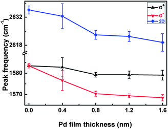 | ||
| Fig. 4 The great changes in the peak frequencies of G+, G− and 2D bands in Raman spectra of monolayer graphene with the increase of Pd film thickness from 0.0 nm to 1.6 nm. | ||
The second important issue here is how to determine the strength of this tensile strain using Raman spectroscopy. In order to evaluate the value of the tensile strain, we have analyzed the changes of peak frequencies of G+, G− and 2D bands with Pd film thickness, which are shown in Fig. 4. To the best of our knowledge, by transferring graphene samples onto transparent flexible substrates, a tensile strain can be introduced into graphene just by stretching the flexible substrate in one direction with a determined distance, so the strain strength can be pre-determined,13–15 which can be further scaled by Raman spectroscopy on the basis of G peak splitting and red Raman shifts of 2D peak. In view of this standpoint, it is not difficult for us to evaluate the strength of Pd-induced strain in graphene based on the difference values (ΔωG = ωG+ − ωG−) between G+ and G− sub-bands as well as 2D peak frequency shifts. Since the difference values ΔωG and Raman shifts of the 2D peak are dependent on Pd film thickness, and have almost no changes with Pd film thickness ranging from 0.8–1.6 nm, we select the mean difference values (∼10.0 cm−1) and red Raman shifts of the 2D peak (∼18.0 cm−1) on the graphene surface as a rough estimation. On one hand, according to the linear relationships of G+ and G− peak frequencies with the applied strain reported by Yoon et al.,25 the following equations can be deducted: (ωG+ − ω0)/ε ≈ −13.7 cm−1/%, (ωG− − ω0)/ε ≈ −33.2 cm−1/%, so we can get the equation to describe the relationship between the difference values and the applied strain: ΔωG/ε = (ωG+ − ωG−)/ε ≈ 19.5 cm−1/%, ε is the strength of strain. Thus, the Pd-induced strain ε is calculated to be around 0.5% just using the difference value 10.0 cm−1. On the other hand, 2D peak frequency shift is another route to obtain the strain strength. Due to the linear relationship between 2D peak frequency and the applied strain:25 Δω2D/ε ≈ 50.0 cm−1/%, the strain strength ε is around 0.4%, which is a little less than that obtained from the difference values ΔωG. This difference in these two values is not avoided, because the reported shift rates of G+, G− and 2D bands are still a matter of scientific dispute. Even so, it is reasonable for us to draw a conclusion that, after thermal evaporation of a Pd film onto graphene, the strength of the tensile strain in graphene is around 0.5%, which is analogous to recently reported results about the physisorption strain between graphene and Cu.16 Meanwhile, at graphene edges, the G peak is also splitting, and the difference value (ΔωG) between G+ and G− sub-bands is above 11.5 cm−1, suggesting that a tensile strain of 0.6% or more at graphene edges is induced by Pd adsorption.
In summary, we have provided an alternative technique to induce a tensile strain in graphene by thermal evaporation of a Pd film onto n-layer graphenes, and performed a systematic Raman study to investigate the strain effects induced at the interface between graphene and Pd, which results in different Raman features among n-layer graphenes. Especially, via Raman spectroscopy-based technique, it is the first time for us to observe the different strain effects between graphene edges (around 0.6%) and central (around 0.5%) regions. This study is of crucial importance for understanding the metal–graphene contact resistance, and the development of high-performance graphene devices.35,36
Acknowledgements
This work was supported by National Science Foundation of China (Grant no. 10774032, 90921001).Notes and references
- A. K. Geim and K. S. Novoselov, Nat. Mater., 2007, 6, 183 CrossRef CAS.
- X. Du, I. Skachko, A. Barker and E. Andrei, Nat. Nanotechnol., 2008, 3, 491 CrossRef CAS.
- A. H. C. Neto, F. Guinea, N. M. R. Peres, K. S. Novoselov and A. K. Geim, Rev. Mod. Phys., 2009, 81, 109 CrossRef CAS.
- G. Giovannetti, P. A. Khomyakov, G. Brocks, V. M. Karpan, J. van den Brink and P. J. Kelly, Phys. Rev. Lett., 2008, 101, 026803 CrossRef CAS.
- K. Nagashio, T. Nishimura, K. Kita and A. Toriumi, Appl. Phys. Lett., 2010, 97, 143514 Search PubMed.
- P. Blake, et al. , Solid State Commun., 2009, 149, 1068 CrossRef.
- A. Venugopal, L. Colombo and E. Vogel, Appl. Phys. Lett., 2010, 96, 013512 CrossRef.
- F. N. Xia, V. Perebeinos, Y. M. Lin, Y. Q. Wu and P. Avouris, Nat. Nanotechnol., 2011, 6, 179 Search PubMed.
- Q. J. Wang and J. G. Che, Phys. Rev. Lett., 2009, 103, 066802 CrossRef CAS.
- E. R. Hsieh and S. S. Chung, Appl. Phys. Lett., 2010, 96, 093501 Search PubMed.
- F. Hüe, M. Hÿtch, H. Bender, F. Houdellier and A. Claverie, Phys. Rev. Lett., 2008, 100, 156602 Search PubMed.
- Y. M. Niquet, C. Delerue and C. Krzeminski, Nano Lett., 2012, 12, 3545 Search PubMed.
- Z. H. Ni, T. Yu, Y. H. Lu, Y. Y. Wang, Y. P. Feng and Z. X. Shen, ACS Nano, 2008, 2, 2301 CrossRef CAS.
- T. Yu, Z. H. Ni, C. L. Du, Y. M. You, Y. Y. Wang and Z. X. Shen, J. Phys. Chem. C, 2008, 112, 12602 CrossRef CAS.
- M. Y. Huang, H. G. Yan, C. Y Chen, D. H. Song, T. F. Heinz and J. Hone, Proc. Natl. Acad. Sci. U. S. A., 2009, 106, 7304 CrossRef CAS.
- R. He, L. Y. Zhao, N. Petrone, K. S. Kim, M. Roth, J. Hone, P. Kim, A. Pasupathy and A. Pinczuk, Nano Lett., 2012, 12, 2408 Search PubMed.
- P. Merino, M. Švec, A. L. Pinardi, G. Otero and J. A. Martín-Gago, ACS Nano, 2011, 5, 5627 CrossRef CAS.
- M. Mavrikakis, B. Hammer and J. K. Nørskov, Phys. Rev. Lett., 1998, 81, 2819 CrossRef.
- M. Zhou, A. H. Zhang, Z. X. Dai, Y. P. Feng and C. Zhang, J. Phys. Chem. C, 2010, 114, 16541 CrossRef CAS.
- H. Q. Zhou, C. Y. Qiu, Z. Liu, H. C. Yang, L. J. Hu, J. Liu, H. F. Yang, C. Z. Gu and L. F. Sun, J. Am. Chem. Soc., 2010, 132, 944 CrossRef CAS.
- Z. T. Luo, L. A. Somers, Y. P. Dan, T. Ly, N. J. Kybert, E. J. Mele and A. T. C. Johnson, Nano Lett., 2010, 10, 777 CrossRef CAS.
- M. J. McAllister, J. L. Li, D. H. Adamson, H. C. Schniepp, A. A. Abdala, J. Liu, M. Herrera-Alonso, D. L. Milius, R. Car, R. K. Prud'homme and I. A. Aksay, Chem. Mater., 2007, 19, 4396 CrossRef CAS.
- T. M. G. Mohiuddin, A. Lombardo, R. R. Nair, A. Bonetti, G. Savini, R. Jalil, N. Bonini, D. M. Basko, C. Galiotis, N. Marzari, K. S. Novoselov, A. K. Geim and A. C. Ferrari, Phys. Rev. B: Condens. Matter Mater. Phys., 2009, 79, 205433 CrossRef.
- L. M. Malard, M. A. Pimenta, G. Dresselhaus and M. S. Dresselhaus, Phys. Rep., 2009, 473, 51 CrossRef CAS.
- D. Yoon, Y. W. Son and H. Cheong, Phys. Rev. Lett., 2011, 106, 155502 CrossRef.
- I. Calizo, A. A. Balandin, W. Bao, F. Miao and C. N. Lau, Nano Lett., 2007, 7, 2645 CrossRef CAS.
- A. A. Balandin, Nat. Mater., 2011, 10, 569 CrossRef CAS.
- D. Teweldebrhan and A. A. Balandin, Appl. Phys. Lett., 2009, 94, 013101 CrossRef.
- G. X. Liu, D. Teweldebrhan and A. A. Balandin, IEEE Trans. Nanotechnol., 2011, 10, 865 Search PubMed.
- I. Calizo, W. Z. Bao, F. Miao, C. N. Lau and A. A. Balandin, Appl. Phys. Lett., 2007, 91, 201904 CrossRef.
- I. Calizo, I. Bejenari, M. Rahman, G. X. Liu and A. A. Balandin, J. Appl. Phys., 2009, 106, 043509 CrossRef.
- E. J. Zeman, K. T. Carron, G. C. Schatz and R. P. V. Duyne, J. Chem. Phys., 1987, 87, 4189 CrossRef CAS.
- Z. H. Zhang, C. F. Chen and W. L. Guo, Phys. Rev. Lett., 2009, 103, 187204 CrossRef.
- P. Lu, Z. H. Zhang and W. L. Guo, Phys. Lett. A, 2009, 373, 3354 CrossRef CAS.
- Z. X. Zhang, Z. Z. Sun, J. Yao, D. V. Kosynkin and J. M. Tour, J. Am. Chem. Soc., 2009, 131, 13460 Search PubMed.
- H. J. Song, M. Son, C. Park, H. Lim, M. P. Levendorf, A. W. Tsen, J. Park and H. C. Choi, Nanoscale, 2012, 4, 3050 RSC.
Footnote |
| † These authors contributed equally to this work. |
| This journal is © The Royal Society of Chemistry 2013 |