Quantum transport through an array of quantum dots
Shuguang
Chen
a,
Hang
Xie
a,
Yu
Zhang
a,
Xiaodong
Cui
b and
Guanhua
Chen
*a
aDepartment of Chemistry, Centre of Theoretical and Computational Physics, The University of Hong Kong, China. E-mail: ghc@everest.hku.hk; Fax: +852 29155176; Tel: +852 28592164
bDepartment of Physics, Centre of Theoretical and Computational Physics, The University of Hong Kong, China
First published on 12th November 2012
Abstract
The transient current through an array of as many as 1000 quantum dots is simulated with two newly developed quantum mechanical methods. To our surprise, upon switching on the bias voltage, the current increases linearly with time before reaching its steady state value. And the time required for the current to reach its steady state value is proportional to the length of the array, and more interestingly, is exactly the time for a conducting electron to travel through the array at the Fermi velocity. These quantum phenomena can be understood by a simple analysis on the energetics of an equivalent classical circuit. An experimental design is proposed to confirm the numerical findings.
Quantum transport has been an important research subject as the feature size of transistors inches towards 10 nm. Much has been understood for the steady state current,1–9 while relatively few investigations have been carried out for time-dependent quantum transport. As it is now common to measure the electric response with nanosecond resolution and with amplitude as little as a few pico-amperes, time-dependent current through nanodevices is becoming a research focus. Several numerical approaches have been developed to simulate the transient currents through molecular and nanoscopic devices.10–15 Most of the studies have been confined to small systems. For instance, a two-terminal one-level device was studied16 and persistent oscillations are observed before the steady state current is reached. It would be interesting to study the transient currents through extensive structures and to investigate the corresponding size effects. Recently the hierarchical equation of motion (HEOM) approach based on the single-particle Liouville–von Neumann equation was proposed.17 As the single-particle Liouville–von Neumann equation is based on the equation of motion (EOM) for the reduced single-electron density matrix (RSDM) rather than the reduced density matrix of the system, its numerical solution is expected to be very efficient so that it can be applied to simulate the transient currents through large devices. In this work, we implement numerically two algorithms proposed in ref. 17, and apply them to study the occurrence of transient current through an extended one-dimensional array of up to one thousand quantum dots (QDs).
We describe briefly the numerical methods before proceeding to the simulation of transient current. The HEOM of the single-particle liouville–von Neumann equation for an electronic device coupled to the electrodes (α) reads,12,17
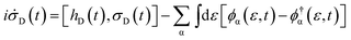 | (1) |
 | (2) |
i![[small phi, Greek, dot above]](https://www.rsc.org/images/entities/i_char_e0a3.gif) α,α′(ε,ε′,t) = −[ε + Δα(t) − ε′ − Δα′(t)]ϕα,α′ + Λα′(ε′)ϕα(ε,t) − ϕ†α′(ε′,t)Λα(ε) α,α′(ε,ε′,t) = −[ε + Δα(t) − ε′ − Δα′(t)]ϕα,α′ + Λα′(ε′)ϕα(ε,t) − ϕ†α′(ε′,t)Λα(ε) | (3) |
According to ref. 17 and 18, the linewidth matrix Λα(ε) of the electrode α can be expanded in terms of multiple Lorentzians as follows,
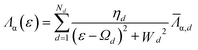
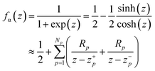
![[capital Lambda, Greek, macron]](https://www.rsc.org/images/entities/i_char_e0bb.gif) α,d is a matrix of the same rank. Fermi distribution function can be expanded via Padé spectrum decomposition,
α,d is a matrix of the same rank. Fermi distribution function can be expanded via Padé spectrum decomposition,where z = β(ε − μα), z+p and z−p are the pth Padé pole in the upper and lower complex plane, respectively. Rp is the corresponding residue in the Padé spectrum decomposition.
With these expansions, the integrals in eqn (1) and (2) can be replaced by the residue summations using the residue theorem, and eqn (1)–(3) become
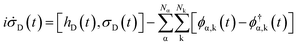 | (4) |
 | (5) |
| iαk,α′k′(t) = −[iγ+α,k + Δα(t) + iγ−α,k − Δα′(t)]ϕαk,α′k′(t) + i[A>−α′,k′ − A<−α′,k′]ϕα,k(t) − iϕ†α′,k′(t)[A>+α,k − A<+α,k] | (6) |
![[small sigma, Greek, macron]](https://www.rsc.org/images/entities/i_char_e0d2.gif) (t) = I − σ(t). ϕα,k(t) and ϕαk,α′k′(t) are the first- and second-tier discrete auxiliary RSDMs, respectively, as defined in ref. 17 and 18. Nα is the number of the electrodes, Nk = Np + Nd is the total number of Lorentzian and Padé spectrum decomposition. A>+α,k, A>−α,k, A<+α,k and A<−α,k are the matrices of the same rank as α,d; γ+α,k and γ−α,k are the coefficients; and their expressions or values are given in ref. 18. We term the solution of eqn (4)–(6) as the Lorentzian–Padé decomposition (LPD) scheme.
(t) = I − σ(t). ϕα,k(t) and ϕαk,α′k′(t) are the first- and second-tier discrete auxiliary RSDMs, respectively, as defined in ref. 17 and 18. Nα is the number of the electrodes, Nk = Np + Nd is the total number of Lorentzian and Padé spectrum decomposition. A>+α,k, A>−α,k, A<+α,k and A<−α,k are the matrices of the same rank as α,d; γ+α,k and γ−α,k are the coefficients; and their expressions or values are given in ref. 18. We term the solution of eqn (4)–(6) as the Lorentzian–Padé decomposition (LPD) scheme.
According to ref. 17, under the wide-band-limit (WBL) approximation, eqn (1)–(3) become
 | (7) |
 | (8) |
 | (9) |
 . This is referred to as the WBL scheme.
Both schemes are implemented. To test their validities, we employ them to simulate the transient current through a single quantum dot (QD), which was previously investigated by Maciejko et al.16 In their work, the linewidth matrix is expressed as a single Lorentzian function, i.e., Λα(ε) = Λ0αW2/(ε2 + W2), where Λ0α is the linewidth amplitude and W is the bandwidth. For comparison, we adopt exactly the same linewidth function or using WBL. At t = 0, an external bias voltage is switched on between the two electrodes L and R, resulting in the transient current through the QD. Denote ΔεL(t), ΔεR(t) and δhD(t) as the energy shifts of L, R and the QD, respectively. Following Maciejko et al.,16 we set δhD(t) = 1/2[ΔεL(t) + ΔεR(t)], and ΔεL(t) = 0 with ΔεR(t) being a step function which is zero for t < 0.
We compare the results of our calculations with those in ref. 16. For the LPD scheme, we set W = 2.5Λ0 and compare the resulting transient current with the corresponding result in ref. 16. For the WBL scheme, we compare its result with the WBL result in ref. 16. As Fig. 1 shows, the transient currents obtained from both schemes reproduce perfectly the results in ref. 16. This confirms the accuracy of both schemes. It is important to point out that both schemes are numerically efficient, and their computation times are proportional to the simulated time. This is obvious as the computational time to integrate each of eqn (4)–(9) is proportional to the simulated time. To integrate eqn (4)–(9) in the time domain, matrix products are required. Computational time scales thus as O(N3) with N being the number of orbitals. Therefore, it is now feasible to simulate the dynamics of the open systems containing thousands of orbitals over a long simulated time.
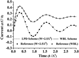 | ||
| Fig. 1 Comparison between the calculated transient currents through a single QD with the LPD and WBL schemes and the results in ref. 16. The current is in the unit of eΛ0/ℏ and time is in the unit of ℏ/Λ0. ΔεR(t) = 10Λ0, kBT = 0.1Λ0, where Λ0 = Λ0L + Λ0R. For the LPD scheme, Lorentzian bandwidth W = 2.5Λ0, and the calculated results (the dashed line) are compared with the corresponding results (filled squares) in ref. 16. For the WBL scheme, its results (solid line) are compared with the corresponding WBL approximation results (open triangles) in ref. 16. | ||
After verifying the validities of both schemes, we apply them to simulate the transient currents through one-dimension array of QDs, which can be described by a tight-binding (TB) Hamiltonian. In the TB system, we consider only the nearest neighbor coupling. The on-site energy is set to zero, and the nearest neighbor coupling matrix element γ is tuned to 10 μeV by varying the voltage of the gate between two neighboring QDs.19 The schematic diagram is shown in Fig. 2. For convenience, we select different numbers of QDs in the middle of an infinite long chain as the device (D), leaving other two semi-infinite parts as the left and right electrodes (L and R). For energy shift, we set ΔεL(t) = 0 and ΔεR(t) as a step function with the bias voltage amplitude of 2 μV (i.e., ΔεR(t < 0) = 0 and ΔεR(t ≥ 0) = 2 μV). Temperature is set to 1.5 mK. Potential varies linearly across the device region.20 All systems containing 1 to 100 QDs in the device region are treated with WBL scheme. For 10 and 100 QDs cases, LPD scheme calculations are also carried out. The results obtained are shown in Fig. 3(a) and (b).
 | ||
| Fig. 2 Schematic diagram of the quantum dots array. The quantum dots are labeled as Dot, and P represents the gate probes used to control the interdots coupling. D, L and R are Device region, left and right side electrode, respectively. QDs of the device region are indexed from 1 to N. | ||
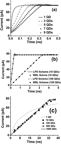 | ||
| Fig. 3 Calculated transient current through the left electrode. (a) Results obtained using WBL scheme for 1, 3, 5, 7, 9 QDs; (b) results obtained using both LPD and WBL schemes for 10 and 100 QDs and (c) rescaled results obtained using the WBL scheme for 1, 10, 100, 500 and 1000 QDs with the horizontal coordinates multiplied by 1000, 100, 10, 2 and 1, respectively. | ||
According to the Landauer–Büttiker formula, the quantum conductance of a single conducting channel is e2/h, where h is the Planck constant and e is the electronic charge. When bias voltage 2 μV is applied, it should result in a steady state current of 77.4 pA. This is exactly what we obtained from both schemes when the steady state current is reached. As shown in Fig. 3(b), because the bias voltage is small and the system is in the linear response region, the two schemes yield almost the same time-dependent currents, which confirms again the accuracy and validity of both schemes.
To our surprise, the transient current grows linearly with respect to time before reaching its steady states value for 100 QDs. This is quite different from the situation of the devices containing a few QDs, as shown in Fig. 3(a). Note that the bias voltage applied here for 1 QD is much smaller than that in Fig. 1, hence the two results differ. The linear relationship between the initial current and time is indeed a size effect. Moreover, longer the array is, more the switch-on time is. In Fig. 3(c), we extend our calculations to as many as 1000 QDs and rescale the simulated times for the array of 1, 10, 100 and 500 QDs by multiplying the corresponding values by 1000, 100, 10 and 2, respectively. It is found that the rescaled results of 100 and 500 QD cases fall onto the same linear line for the 1000 QDs result. This confirms that the switch-on time is exactly proportional to the length of the QD array for a large system. The I–t (current versus time) curve is linear for very long QD arrays while it is exponential-like (i.e. I(t) ≈ I0(1 − e−at)) for the 1 QD system. The I–t curve of 10 QDs case is quite linear with some slight deviation as compared to those of 100, 500 and 1000 QDs. Fig. 3(c) clearly shows the discrepancy between the small and large systems in terms of increasing transient current.
It should be pointed out that the current oscillation is related to the bias voltage and the coupling strength. For the 1 QD system, as shown in Fig. 4(a), when the bias voltage is enhanced to an extremely high value over 2 mV, current oscillations begin to occur. Since all our previous calculations in Fig. 3 are carried out under low bias voltages, the current oscillation is small. To explore the generality of the linear relationship between current and time for large systems, we increase the bias voltage for 100 QDs, and the results are shown in Fig. 4(b). The initial linear relationship between current and time survives for a very high bias voltage V = 0.4 mV with its characteristic electron energy being 40 times of the linewidth. This confirms that the linear relationship between current and time is a general phenomenon. When the bias voltage is further enhanced to an extremely high value over 0.8 mV, oscillations begin to occur. However, in such circumstances, the electronic structure is distorted so much by the extremely strong external field that the transmission coefficients become very small and the I–t curve becomes drastically different from those with the bias voltages less than 0.4 mV. As shown in Fig. 4(b), larger bias voltage results in higher oscillation frequency and hence undermines the linearly increasing phenomenon. The reason will be discussed at the end of this article. To further investigate the generality of the linear relationship between current and time, an interface scattering is introduced by decreasing or increasing the coupling strength between the device and electrodes. As shown in Fig. 4(c), oscillations could be observed in I–t curves of the 100 QDs system when coupling strength is too high or too low. However, the linear relationship between current and time survives before the maximum value of the current is reached.
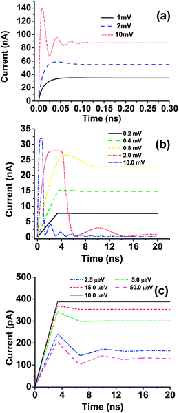 | ||
| Fig. 4 Transient current obtained by using WBL scheme with different bias voltages and coupling strengths between the device and electrode. (a) Transient currents of single QD system with bias voltage equals to 1 mV, 2 mV and 10 mV, respectively; (b) transient currents of 100 QDs system with bias voltage equals to 0.2 mV, 0.4 mV, 0.8 mV, 2.0 mV and 10.0 mV, respectively and (c) transient currents of 100 QDs system with coupling strength between device and electrodes equals to 2.5 μeV, 5.0 μeV, 15.0 μeV and 50 μeV, respectively. The result of the original 10 μeV case is also plotted. | ||
The linear relationship between the initial current and time is robust and survives for very high bias voltages and varying device-electrode couplings or interface scattering between the device and electrodes. This is indeed a size effect, and holds only for longer QD arrays. It can be understood by a simple analysis of energetics involved. As pointed out in ref. 20 and 21, the dynamic electric response of a coherent metallic wire can be mapped onto an equivalent circuit consisting of a kinetic inductor with the inductance L = (Nℏ2π)/(e2γ). The energy of the current passing the metallic wire is stored in the inductor, and can be expressed as

On the other hand, the current passes through a bias voltage V, and the power it requires is P = IV. Equating the changing rate of the energy stored in the inductor with the electric power P, we have
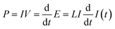
 | (10) |
When a step-shaped bias voltage is applied, the RHS of eqn (10) is a constant after the bias voltage is switched on, and as a result, the time derivative of the transient current is also a constant, which explains the linear relationship between current and time. Here, energy conservation plays a crucial role in the above derivations and guarantees the linearly increasing phenomenon.
According to the Landauer–Büttiker formula, the steady state current of a single channel system under small bias voltage is expressed as

The switch-on time τswitch can be calculated as
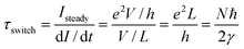 | (11) |
As N is the number of QDs, the switch-on time is proportional to the length, which explains the finding shown in Fig. 3(c).
For the one-dimensional tight-binding system above, the dispersion relation is as follows:
| E(k) = −2γcos(ka) |
where kf is the wave number corresponding to the Fermi energy. As the QDs are half-filled, kf can be determined as follows,
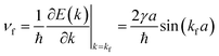
| 0 = E = −2γcos(kfa) |
Thus, we have

As there are N QDs in the array, the first passage time τfp, i.e., the time that a conducting electron needs to travel through the system, can be expressed as
 | (12) |
This is exactly the switch-on time τswitch [see eqn (11)]. Take 100 QDs for example, τfp = 3.3 ns, which is the same with the switch-on time shown in Fig. 3(b). Note that the energy analysis presented here applies to the low frequency or long time dynamics where energy conservation holds over the time period of interest. When an array is short enough, the first passage time τfp is small. According to the Heisenberg uncertainty principle, the time-energy uncertainty relationship can be expressed as δEδt ∼ ℏ/2. Since the feature time for the short arrays (i.e. first passage time) is small, the inequality in the above relationship results in a large quantity of uncertainty of the energy, hence rendering energy conservation invalid. This explains the difference between small and large systems. Similarly, for long QDs arrays, when bias voltage is high enough, the period of the current oscillation becomes so short that it replaces the relatively long τfp to be the feature time of the system, which renders the energy conservation invalid according to the uncertainty principle, and therefore undermines the linearly increasing phenomenon as shown in Fig. 4(b).
Previous research reveals that when confined to a small system, the transient current occurs in a nonlinear way with respect to time. While our work indicates that when the metallic array or wire is long enough, the linear relationship between the coherent current and time emerges. The qualitative difference between the short and long metallic wires is striking, and the size does matter! This is precisely what many researchers in the field of nanoscience are looking for. This kind of size effect, if can be experimentally testified, may help us understand more about the electrical properties of nanostructures thus benefiting the development of nanodevices with new features. In the proposed experiment setup, the current amplitude can be tuned as well by adjusting the bias voltage. To effectively measure the transient current shown in Fig. 3(c), equipment with current resolution of tens of pA with time resolution of ns is required. Such resolutions can be achieved by employing existing commercial instruments. For example, with a combination of an ultrahigh bandwidth current–voltage converter (FEMTO HAS) and a high speed voltage amplifier (ORTEC FTA820A), the current signal of 10 pA can be transferred into 0.1 mV voltage, at the effective bandwidth of 2 GHz, which could be easily detected by ultra high-speed oscilloscopes.
Support from the Hong Kong Research Grant Council (Contract Nos. HKU7009/09P, 7008/08P, 7007/11P, and HKUST 9/CRF/08) and the University Grant Council (Contract no. AoE/P-04/08) is gratefully acknowledged.
References
- R. Landauer, IBM J. Res. Dev., 1957, 1, 223 CrossRef.
- S. Datta, Electronic Transport in Mesoscopic Systems, Cambridge University Press, 1997 Search PubMed.
- Y. Q. Xue, S. Datta and M. A. Ratner, J. Chem. Phys., 2001, 115, 4292 CrossRef CAS.
- J. Taylor, H. Guo and J. Wang, Phys. Rev. B: Condens. Matter Mater. Phys., 2001, 63, 245407 CrossRef.
- H. J. Dai, E. W. Wong and C. M. Lieber, Science, 1996, 272, 523 CAS.
- M. Bütiker, Y. Imry, R. Landauer and S. Pinhas, Phys. Rev. B: Condens. Matter Mater. Phys., 1985, 31, 6207 CrossRef.
- P. Guyot-Sionnest, J. Phys. Chem. Lett., 2012, 3, 1169 CrossRef CAS.
- D. Mann, A. Javey, J. Kong, Q. Wang and H. J. Dai, Nano Lett., 2003, 3, 1541 CrossRef CAS.
- Z. Xu, Q.-S. Zheng and G. Chen, Appl. Phys. Lett., 2007, 90, 223115 CrossRef.
- A.-P. Jauho, N. S. Wingreen and Y. Meir, Phys. Rev. B: Condens. Matter Mater. Phys., 1994, 50, 5528 CrossRef CAS.
- S. Kurth, G. Stefanucci, C. O. Almbladh, A. Rubio and E. K. U. Gross, Phys. Rev. B: Condens. Matter Mater. Phys., 2005, 72, 035308 CrossRef.
- X. Zheng, F. Wang, C. Y. Yam, Y. Mo and G. Chen, Phys. Rev. B: Condens. Matter Mater. Phys., 2007, 75, 195127 CrossRef.
- J. Yuen-Zhou, D. G. Tempel, C. A. Rodriguez-Rosario and A. Aspuru-Guzik, Phys. Rev. Lett., 2010, 104, 043001 CrossRef.
- S.-H. Ke, R. Liu, W. Yang and H. U. Baranger, J. Chem. Phys., 2010, 132, 234105 Search PubMed.
- V. Moldoveanu, V. Gudmundsson and A. Manolescu, Phys. Rev. B: Condens. Matter Mater. Phys., 2007, 76, 085330 CrossRef.
- J. Maciejko, J. Wang and H. Guo, Phys. Rev. B: Condens. Matter Mater. Phys., 2006, 74, 085324 CrossRef.
- X. Zheng, G. H. Chen, Y. Mo, S. K. Koo, H. Tian, C. Yam and Y. J. Yan, J. Chem. Phys., 2010, 133, 114101 CrossRef.
- H. Xie, F. Jiang, H. Tian, X. Zheng, Y. Kwok, S. chen, C. Yam, Y. Yan and G. Chen, J. Chem. Phys., 2012, 137, 044113 CrossRef.
- F. R. Waugh, M. J. Berry, D. J. Mar, R. M. Westervelt, K. L. Campman and A. C. Gossard, Phys. Rev. Lett., 1995, 75, 705 CrossRef CAS.
- C. Y. Yam, Y. Mo, F. Wang, X. B. Li, G. H. Chen, X. Zheng, Y. Matsuda, J. Tahir-Kheli and W. A. Goddard, Nanotechnology, 2008, 19, 495203 CrossRef.
- P. J. Burke, IEEE Transactions on Nanotechnology, 2003, 2, 55 CrossRef.
| This journal is © The Royal Society of Chemistry 2013 |