Graphene nanoribbon electrical decoupling from metallic substrates
Ivo
Borriello
a,
Giovanni
Cantele
*b and
Domenico
Ninno
ab
aUniversità di Napoli “Federico II”, Dipartimento di Scienze Fisiche, Complesso Universitario Monte Sant'Angelo, Via Cintia, I-80126 Napoli, Italy
bCNR-SPIN, Complesso Universitario Monte Sant'Angelo, Dipartimento di Scienze Fisiche, Via Cintia, I-80126 Napoli, Italy. E-mail: giovanni.cantele@spin.cnr.it
First published on 2nd October 2012
Abstract
We address the structural and electronic properties of graphene nanoribbons (GNRs) covalently immobilized on a metallic substrate by means of an organic layer. The GNR–organic layer and organic layer–metal interfaces can be thought of as constituents of a nanodevice and have been accurately studied using large-scale density functional theory calculations. Our results demonstrate the possibility of combining nanopatterned metal–organic layer substrates with selected GNRs to obtain well ordered and stable structures while preserving the GNR energy band gap, an essential requirement for any switching nanodevice.
1 Introduction
Because of the remarkable and unprecedented properties related to its honeycomb lattice, graphene has emerged as a fascinating system for fundamental studies in condensed matter physics, as well as a promising candidate material for applications in nanoelectronics.1–5 However, graphene, unlike standard semiconductors, has a zero energy band gap making the realization of a switching device impossible. One route to circumvent this problem is to shape graphene into strips known as nanoribbons (GNRs). Quantum confinement in GNR channels about 1 nm wide induces band gaps of the order of ∼1 eV. Tunable properties that depend on the width and direction of the ribbon relative to the graphene lattice are also predicted6 and experimentally observed.7,8 Nevertheless, the electronic properties of GNRs might be hindered, degraded or modified if precise control of the edges is not achieved.5 Only recently, the possibility of fabricating atomically precise GNRs has been experimentally demonstrated.9Another interesting route for tuning the GNR properties is that of using chemical functionalization. A precise control of the local chemistry of either defects or adsorbed chemical species10–12 is now recognized as a powerful and effective tool for tailoring the structure and properties of carbon-based nanomaterials.13,14 For example, it has been shown that a tunable band gap in quasi-free standing graphene on gold can be reversibly induced using hydrogenation: the size of the gap can reach values as large as ∼1 eV for a hydrogen coverage of 8%.15
The feasibility of graphene-based switching devices is not only related to the precise fabrication of narrow GNRs with a significant energy band-gap, but also to the achievement of a stable immobilization of GNRs on a substrate under working conditions. For example, Cai et al. have recently developed an easy way to produce very narrow armchair nanoribbons with a controllable width (and band-gap), characterized by hydrogen-terminated edges inherited by the molecular precursors.9 The resulting GNRs are physisorbed on a metal surface and can be easily stamp transferred on other substrates. Nevertheless, the substrate-physisorbed GNRs can be easily removed by solvent wash or sonication, tracing us back to the second key point that is the channel stability under working conditions.
In this work we present extensive large-scale first-principles calculations aimed at shedding light on how it is possible to achieve a stable immobilization of GNRs on a metal substrate while preserving their electronic properties. The starting point of our work has been partly inspired by a recent experimental outcome16–19 that demonstrates a novel technique for the covalent immobilization of graphene on both insulating and metallic substrates. By using a thiol-functionalized perfluorophenyl azide (PFPA) as a coupling agent, the covalent anchoring of graphene to a substrate is made possible by a simple heat treatment under ambient conditions, providing a facile approach for the construction of graphene-based nanodevices.
Our work addresses two fundamental aspects which are still controversial and debated in the literature, namely, how and to what extent the presence of both the substrate and the covalent functionalization of the GNR affects the device electronic properties. The formation of the metal–PFPA and PFPA–GNR interfaces might induce significant modifications in the electronic levels as well as in other properties such as the work function, the availability of states at the Fermi level, the n- and p-type conductance, and so on. Therefore, it is of utmost importance, for predicting the device properties under working conditions, to understand the electronic level line-up occurring at the interfaces (e.g. the position of the molecular layer highest occupied and lowest unoccupied states with respect to the metal Fermi level and the GNR band edges).
Following the experimental outcomes of Liu and Yan,16–18 the structure we have studied, sketched in Fig. 1, is composed of a gold substrate to which GNRs are anchored by means of PFPA. It is worth stressing that although the structure showed in this figure has not yet been realized, the possible technical issues in its realization are, at least in principle, covered by the PFPA-based techniques that were originally conceived as a means to derivatize graphene with well defined functional groups, to fabricate graphene films and GNRs and to generate patterned graphene structures by photolithography.
 | ||
| Fig. 1 (a) Top view of an armchair GNR covalently linked to the Au (111) surface through PFPA (the in-plane supercell is also represented). (b) Schematic view of the two possible PFPA–GNR link mechanisms (see text): insertion (I) and addition (II). The side views of the resulting Au–PFPA–GNR systems are given in (c) and (d), respectively. | ||
The calculations are performed in the framework of density functional theory (DFT), which is well known to provide atomistic and chemically accurate descriptions of a wide class of materials and interfaces. We characterize the electronic and structural properties of this new kind of heterojunctions, focusing on the role played by the molecular layer on the electronic levels line-up and on its implications in charge carrier injection and transport.
2 Methods
First principles calculations have been performed in the framework of DFT, as implemented in the Quantum-Espresso package.20 The code uses pseudopotentials to mimic the ion cores and plane waves to represent both the wave functions and the electronic charge densities. The exchange-correlation functional entering the Kohn–Sham equations is chosen within the generalized gradient approximation (GGA) with the PBE parametrization.21 Ultrasoft pseudopotentials22 ensure converged properties (structure, electronic level, etc.) with 40 Ry and 400 Ry cutoffs for the wave functions and the total charge density respectively.The Au–PFPA–GNR heterostructures are described using a supercell. The Au substrate is formed by 5 atomic planes which turned out to be sufficient to ensure converged interface properties with respect to the metallic slab thickness. The link between the Au substrate and the GNR is ensured, on the metal side, by the thiol termination of PFPA, and on the GNR side by a terminal nitrogen atom of the same molecule (see Fig. 1). With the aim of pointing out the effects of both the formation of covalent bonds (which alter the GNR sp2 network) and the presence of the interface on the GNR electronic levels near the Fermi energy, we have considered armchair GNRs (AGNRs) with the edges terminated by hydrogen atoms. Due to quantum confinement, an energy gap shows up in this type of GNRs. For the study of the Au–PFPA–AGNR heterostructure, the AGNR lattice parameter has been stressed (less than 3%) in order to fit the AGNR structure to the metal unit cell. Due to the computational cost, only an AGNR composed of 7 dimer rows parallel to the ribbon axis (see Fig. 1a) has been considered in the calculations. Periodic replicas of the heterostructure in the direction orthogonal to the surface are separated by a 15 Å vacuum space for avoiding spurious interactions. The surface Brillouin zone is sampled with a 1 × 2 × 1 Monkhorst–Pack k-point grid.
The equilibrium geometries have been obtained by fully optimizing all the atomic positions within the surface supercell, until all the components of the residual forces were less than 10−3 a.u. and the energy difference between two consecutive relaxation steps was less than 10−4 a.u. Since the heterointerface is simulated at only one side of the metal slab, a dipole correction has been added to eliminate the effects of spurious electric fields.23
3 Results
The formation of ordered patterns of AGNRs on the metal substrate by means of the covalent immobilization requires, as a first step, the knowledge of the most energetically favorable binding sites of PFPA on AGNR. In order to better understand this point it is worth briefly discussing the link mechanism. The functionalization of carbon materials through photochemically activated PFPA can be depicted as follows.16–18 Upon light (or heat) activation, the PFPA molecules are first converted to the highly reactive singlet perfluorophenyl nitrene. Subsequently, two reaction processes of the perfluorophenyl nitrene with the AGNR can take place. The first is the CH insertion where the N atom is chemically inserted between two bonded C–H atoms at the nanoribbon edge, giving rise to C–N–H as in Fig. 1b, Scheme I. The second is the C![[double bond, length as m-dash]](https://www.rsc.org/images/entities/char_e001.gif) C addition where the N atom links to a CC dimer with the formation of a C–N–C cycle as in Fig. 1b, Scheme II. Both are characterized by the formation of a covalent bond. However, at variance with the insertion, the addition causes the rehybridization (mainly sp2 to sp3) of the carbon atoms.
C addition where the N atom links to a CC dimer with the formation of a C–N–C cycle as in Fig. 1b, Scheme II. Both are characterized by the formation of a covalent bond. However, at variance with the insertion, the addition causes the rehybridization (mainly sp2 to sp3) of the carbon atoms.
Since AGNRs are characterized by singly hydrogenated edge atoms, the insertion is possible only at the edge. On the other hand, the addition can involve any pair of first neighbor carbon atoms (“dimers”), with the carbon–carbon bond running either parallel to or across the ribbon axis direction. Focusing on the AGNR shown in Fig. 2a, the dimer rows parallel to the ribbon axis are labelled by integer numbers starting from the center. For each non equivalent dimer inside the supercell, we consider the sp2 → sp3 rehybridization following the addition of PFPA and, for the sake of comparison, of the –H and –CH2 radicals. A view of the different functionalizations is shown in Fig. 2b for –H, Fig. 2c for –CH2 and Fig. 2d for PFPA. For each functionalization, the total energy of the system where the addition has occurred at the central dimer (labelled as “0” in Fig. 2a) has been taken as the reference energy. In Fig. 2e we show the relative formation energy (RFE)† as a function of the reaction site (carbon dimer) position. In the case of PFPA, the RFE has been computed also for the insertion configuration and is reported in Fig. 2e as a black filled circle. It is evident from Fig. 2e that the RFE does not depend on the particular functionalization, revealing that the binding is locally controlled by the rehybridization of the C atoms. More importantly, edge dimers are the most favored sites for the addition, with an energy gain, with respect to the central dimer, of ∼1 eV. Moreover, as it can be seen from Fig. 2e, the insertion is more favored (by ∼1 eV) than the addition at the edge. It is worth mentioning that the identification of the most favorable binding sites for the covalent functionalization is a fundamental step for the design of well ordered and stable structures, providing insightful indications of the patterns (density, geometry) of organic molecules onto the substrate.
![(a) Top view of the AGNR composed of 7 carbon–carbon dimer rows: the numbers label the dimer lines parallel to the ribbon axis (vertical direction), starting from the centre. (b–d) Schematic view of the sp2 → sp3 rehybridization of a C–C dimer following an addition reaction involving three different functionalizations: –H (b), –CH2 (c), and –PFPA (d). (e) The relative formation energy (RFE) for the three systems depicted in (b–d), as a function of the reaction site (the lines are guides for the eyes). The reference energy, for each functionalization, is given by the system where the reaction has occurred at the innermost dimer [marked as “0” in panel (a)]. The filled circle gives the RFE for the insertion reaction at the AGNR edge for the –PFPA functionalization. On the horizontal axis, integer (half-integer) numbers label carbon dimers running parallel to (across) the ribbon axis. The (empty rectangle) histograms in the insets show the C–C bond length distribution, for the –PFPA functionalization (compared with the pristine AGNR, red-filled rectangles).](/image/article/2013/NR/c2nr31937c/c2nr31937c-f2.gif) | ||
| Fig. 2 (a) Top view of the AGNR composed of 7 carbon–carbon dimer rows: the numbers label the dimer lines parallel to the ribbon axis (vertical direction), starting from the centre. (b–d) Schematic view of the sp2 → sp3 rehybridization of a C–C dimer following an addition reaction involving three different functionalizations: –H (b), –CH2 (c), and –PFPA (d). (e) The relative formation energy (RFE) for the three systems depicted in (b–d), as a function of the reaction site (the lines are guides for the eyes). The reference energy, for each functionalization, is given by the system where the reaction has occurred at the innermost dimer [marked as “0” in panel (a)]. The filled circle gives the RFE for the insertion reaction at the AGNR edge for the –PFPA functionalization. On the horizontal axis, integer (half-integer) numbers label carbon dimers running parallel to (across) the ribbon axis. The (empty rectangle) histograms in the insets show the C–C bond length distribution, for the –PFPA functionalization (compared with the pristine AGNR, red-filled rectangles). | ||
The RFE trend shown in Fig. 2e is easily explained in terms of the structural distortion induced by the carbon rehybridization. The histograms with empty rectangles in the insets of Fig. 2e show, for each site, the typical C–C bond length distribution in the presence of addition. These histograms must be compared with those red-filled that correspond to the pristine AGNR.‡ It is seen that the less stable systems (higher RFE) are characterized by a pronounced variation of the carbon–carbon bond lengths. On the other hand, the insertion at the edge causes minor structural differences compared to the pristine AGNR.
Once it has been established that for both insertion and addition the most favored sites for the PFPA binding are those at the AGNR edge, the next step is that of studying the effects of the resulting interface on the AGNR electronic properties. Band structure calculations for the entire structure show that the AGNR energy band gap does not collapse, although the actual magnitude may have some variation. In Fig. 3 we show the calculated band structure for the pristine AGNR, with edge carbon atoms either single hydrogenated (panel a) or double hydrogenated (panel b). These band structures serve as a reference for the discussion of the heterointerface electronic structure. Panels (c) and (d) show the projection of the full Au–PFPA–AGNR band structure on the AGNR atomic orbitals, for the insertion and addition respectively. The size of the dots is proportional to the projection amplitude.
 | ||
| Fig. 3 (a) Band structure of the pristine AGNR shown in Fig. 2a. Red (blue) lines represent occupied (unoccupied) states. (b) Band structure of the pristine AGNR with one out of two edge carbon dimers double-hydrogenated. (c and d) Au–PFPA–AGNR band structure projected onto all the AGNR atomic orbitals (black dots) for the (c) insertion and (d) addition configurations (due to steric effects, only one out of two edge carbon dimers is involved in the case of the addition). The size of the dots is proportional to the projection (with the largest dots corresponding to a projection of ≥90%). In (c) the solid lines represent the band structure of the hydrogenated AGNR whose atomic positions are the same as those of the anchored AGNR in the Au–PFPA–AGNR system with insertion (see text). EF and EV are the Fermi level and the valence band maximum respectively. Notice that the zero energy is taken at the GNR top valence band in (a) and (b) but at the metal-pinned Fermi level in (c) and (d). | ||
Inspecting the four panels of Fig. 3 we can draw the following two points. The first is that the band structure with insertion (panel c) has a reduced but still significant band gap with respect to the pristine AGNR. Some other differences can be ascribed to the geometrical distortions induced by the covalent bonding, but not to electronic processes (such as charge transfer) occurring at the interface. Indeed, in the same panel (c) we report, as blue and red solid lines, the band structure of an isolated AGNR whose atomic positions are the same as those of the anchored AGNR. The almost full overlap between the two band structures provides strong evidence of the above conclusion.
The second point concerns the addition that, for its nature, causes a number of edge carbon atoms to be four-fold coordinated, thus changing their hybridization. We therefore expect that the resulting bands should closely resemble those of the 7-AGNR with double-hydrogenated carbon atoms. Indeed, the comparison of panels (b) and (d) (both corresponding to one out of two edge dimers with double passivation) shows a remarkable agreement between the two. It should be pointed out that the presence of four-fold coordinated edge atoms causes a band gap reduction and a change of the overall band structure, as is easily seen if we compare panels (b) and (d) with panels (a) and (c). The gap reduction is directly linked with the change of the AGNR aromaticity caused by the edge rehybridization.24,25
To provide a more physical insight into the electronic properties at the interface we have carried out an accurate analysis of the spatial distribution of the electronic orbitals as a function of the energy. The topical result is shown in Fig. 4, top-left panel, where the local density of states (LDOS) is shown for the Au–PFPA–AGNR heterointerface in the insertion configuration. The LDOS plot sheds light on two main issues, noteworthy for the engineering of nanoscale transport devices. Firstly, there is no interface-induced doping of the AGNR. The Fermi energy is pinned by the metal and falls into the AGNR band gap. Secondly, in an energy range of ∼3 eV around the Fermi energy there are no electronic states with at least part of the electron density localized on the PFPA layer. This also emerges from the contour plots of the LDOS at the AGNR HOMO and LUMO energies (panels labelled respectively with (4) and (5) in Fig. 4), where it is clearly visible as the PFPA acts as an insulating layer, with no charge density leakage from/to either the metal or the AGNR. This result indicates that the formation of the interface should not alter significantly the AGNR transport properties.§
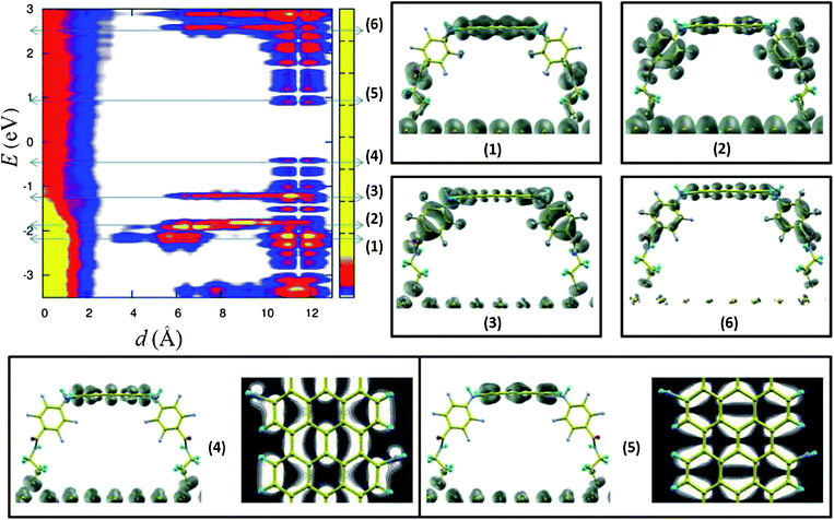 | ||
| Fig. 4 (top left) LDOS for the Au–PFPA–AGNR heterostructure (insertion configuration). The zero of the abscissa corresponds to the last Au layer. The regions of significantly non-zero LDOS are highlighted by the color scale, with the maximum (yellow) obviously located on the metal side. The PFPA organic layer fits in the distance range between ∼1.5 Å and ∼11 Å, whereas the AGNR is located at about ∼11.5 Å. Labels (1) to (6) identify specific energy levels, in particular: (1) ⇒ Au–PFPA bonding, (2) ⇒ PFPA–AGNR bonding, (3) ⇒ PFPA–HOMO, (4) ⇒ AGNR–HOMO, (5) ⇒ AGNR–LUMO, and (6) ⇒ PFPA–LUMO. The charge density contours corresponding to these energy levels are shown in the panels with the same labels. Additional planar projections of the AGNR HOMO and LUMO are given in (4) and (5). The Fermi level of the whole system is pinned by the metal and is set to zero. | ||
From the same figure we can also appreciate the spatial localization of the PFPA HOMO and LUMO orbitals (see the panels labelled respectively with (3) and (6) and their energies in the LDOS plot), as well as the highest-energy orbitals involved in the metal–PFPA and PFPA–AGNR covalent bond formation (see the panels labelled respectively with (1) and (2) and their energies in the LDOS plot).
The previous findings allow us to conclude that no net charge transfer occurs which indeed would result in a “doping” of the AGNR. Since the Fermi level is pinned by the metal, upon formation of the metal–PFPA–AGNR interface we expect a modification of the relative alignment of the PFPA and AGNR electronic levels with respect to the metal Fermi level. However, such an alignment must be accompanied by a redistribution of the overall electronic charge density that, because of the Fermi level pinning, is due to the formation of a series of microscopic dipole moments. Such phenomena have been found in hybrid organic–inorganic interfaces, such as self-assembled monolayer (SAM) on metal substrates29,30 or organic adsorbates on semiconductor surfaces.31,32
To clarify this important point, the electronic charge redistribution Δρtot following the formation of the metal–PFPA and PFPA–AGNR interfaces has been calculated as the difference between the (self-consistent) charge density of the full metal–PFPA–AGNR system (ρtot) and the (self-consistent) charge densities of the “isolated” components. These components are the PFPA once the layer of H atoms involved in the formation of the S–Au and N–C bonds has been removed (ρPFPA–ρH), the metal slab (ρmetal), and the AGNR (ΔρAGNR). In other words, Δρtot = ρtot − ρPFPA − ρmetal − ρAGNR + ρH.¶ After some simple algebra, the expression for ρtot can be recasted by separating different contributions: Δρtot = Δρmetal–PFPA + ΔρPFPA–AGNR + ΔρSDL. The first two terms, Δρmetal–PFPA and ΔρPFPA–AGNR describe the charge density redistribution due to the formation of the chemical bonds at the “isolated” metal–PFPA and PFPA–AGNR interfaces. In the presence of a single interface, for example metal–PFPA, this redistribution is responsible for variations of the substrate work function which cannot be attributed to the net dipole moment carried out by the isolated organic layer.29,30 The third contribution, ΔρSDL, that will be referred to as the space dipole layer (SDL) contribution, is related to the co-presence of the two interfaces. At variance with the first two ones, that are usually (but not always) localized within very few atomic layers around the interface (with no long-range tails), ΔρSDL, if not zero, is responsible for the additional field needed to “match” the levels at the double interface. Moreover, while Δρmetal–PFPA and ΔρPFPA–AGNR have a purely chemical nature (being associated with the formation of a chemical bond), ΔρSDL has a “thermodynamic” origin. An insightful example is provided by the well known silicon p–n junction: here, the left and right Fermi level alignment occurs through the formation of a space charge layer. Nevertheless, the presence of free carriers (electrons and holes) in the doped silicon regions makes such an alignment to occur through a net charge transfer resulting from the migration of electrons and holes from one side to the other. Instead, for the metal–PFPA–AGRN junction, the “insulating” character of the two interfaces (that is, net transfer of electronic charges is not possible in this case) makes the additional level alignment needed to match the Fermi levels of the “left” (metal–PFPA) and “right” (PFPA–AGNR) regions to occur through the PFPA layer “polarization”: a sequence of microscopic dipoles across the molecule occurs, resulting in a net dipole moment whose magnitude depends on how “far” the levels of the isolated interfaces are prior to the formation of the double interface.
In support of this interpretation, in Fig. 5 we show the planar average of ΔρSDL as a function of the coordinate in the direction orthogonal to the metal surface (the average is taken on planes parallel to the surface). The “sequence” of microscopic dipole moments, which describe the polarization of the PFPA bonds, is clearly visible for both the addition and the insertion configuration. The resulting electrostatic potential ΔSDL is also shown.|| It is clear that the SDL potential provides the additional step needed for the “left” and “right” electronic levels to be aligned. Nevertheless, the magnitude of this step is strongly dependent on the considered system: 0.747 eV for the insertion configuration, to be contrasted with 0.063 eV for the addition configuration. The one order of magnitude difference is attributed to the different chemistry (chemical bonds, see Fig. 1b) and electronic structure (energy gap, see Fig. 3c and d) of the two systems.
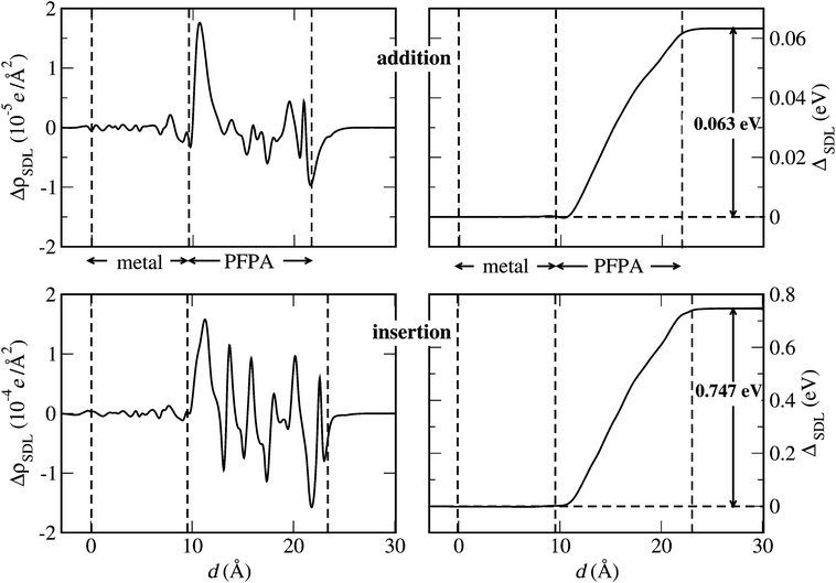 | ||
| Fig. 5 The total charge density redistribution ΔρSDL (left panels) and the resulting electrostatic potential ΔSDL (right panels) associated with the SDL formation at the double metal–PFPA–AGNR interface. Both the addition (upper panels) and the insertion (lower panels) configurations are shown. The zero on the horizontal axis corresponds to the first metal layer. | ||
4 Discussion and conclusions
In this work we have presented extensive DFT calculations to investigate the nature of the metal–PFPA–AGNR interface and its implications in graphene-based nanodevices. The main outcomes can be summarized as follows:i. Formation energy calculations reveal that armchair edge carbon dimers are preferred for the covalent binding of PFPA-molecules. This suggests possible patterning schemes of substrates for realizing regular and reproducible anchoring configurations of GNRs. We believe that the techniques that are now available to experiments16–18 can be a good starting point.
ii. The covalent immobilization of the GNR can occur in at least two configurations that differ for the chemical modification induced by the covalent bonding at the GNR edges. However, the occurrence of a significant band gap is not compromised by such modifications.
iii. The metallic substrate determines the pinning of the Fermi level without any doping effect.
iv. The organic layer acts as an insulator, giving a substantial electrical decoupling between the metal and GNR electronic states.
v. The metal–PFPA–AGNR electronic level line-up is interpreted in terms of a space dipole layer across the PFPA linker. In particular, once the “left” (metal–PFPA) and “right” (PFPA–AGNR) interface electronic levels have been determined, the additional step required for the Fermi level to fall within the AGNR energy gap is provided by an electrostatic potential step generated by a sequence of microscopic dipoles (that in turn describe the polarization of the PFPA bonds).
We believe that our results indicate a route for the realization of GNR-based nanodevices and highlight the role of the local chemistry in the performance and functionality of such devices.10,11,33 As a final remark, we would like to suggest the use of nanopatterned substrates characterized by regularly separated metal chains whose role is that of being linking points for thiolated-PFPA. Lines of molecules at a suitable distance can be combined with selected bottom-up nanoribbons for maximizing the probability of edge-bond formation. The organic linker might have the additional advantage of electrically minimizing the substrate effects.34,35
Acknowledgements
We acknowledge the CINECA award under the ISCRA initiative, for the availability of high performance computing resources. Financial support from the European Union Seventh Framework Program (FP7/2007–2013) under grant agreement no. 264098-MAMA is acknowledged.References
- K. Novoselov, A. Geim, S. Morozov, D. Jiang, Y. Zhang, S. Dubonos, I. Grigorieva and A. Firsov, Science, 2004, 306, 666–669 CrossRef CAS.
- A. K. Geim and K. S. Novoselov, Nat. Mater., 2007, 6, 183–191 CrossRef CAS.
- A. K. Geim, Science, 2009, 324, 1530–1534 CrossRef CAS.
- P. Avouris, Nano Lett., 2010, 10, 4285–4294 CrossRef CAS.
- F. Schwierz, Nat. Nanotechnol., 2010, 5, 487–496 CrossRef CAS.
- L. Yang, C.-H. Park, Y.-W. Son, M. L. Cohen and S. G. Louie, Phys. Rev. Lett., 2007, 99, 186801 CrossRef.
- B. Oezyilmaz, P. Jarillo-Herrero, D. Efetov and P. Kim, Appl. Phys. Lett., 2007, 91, 192107 CrossRef.
- Y.-M. Lin, V. Perebeinos, Z. Chen and P. Avouris, Phys. Rev. B: Condens. Matter Mater. Phys., 2008, 78, 161409 CrossRef.
- J. Cai, P. Ruffieux, R. Jaafar, M. Bieri, T. Braun, S. Blankenburg, M. Muoth, A. P. Seitsonen, M. Saleh, X. Feng, K. Muellen and R. Fasel, Nature, 2010, 466, 470–473 CrossRef CAS.
- K. P. Loh, Q. Bao, P. K. Ang and J. Yang, J. Mater. Chem., 2010, 20, 2277–2289 RSC.
- T. M. Swager, ACS Macro Lett., 2012, 1, 3–5 Search PubMed.
- F. Buonocore, F. Trani, D. Ninno, A. Di Matteo, G. Cantele and G. Iadonisi, Nanotechnology, 2008, 19, 025711 Search PubMed.
- A. V. Krasheninnikov and F. Banhart, Nat. Mater., 2007, 6, 723–733 CrossRef CAS.
- F. Banhart, J. Kotakoski and A. V. Krasheninnikov, ACS Nano, 2011, 5, 26–41 CrossRef CAS.
- D. Haberer, D. V. Vyalikh, S. Taioli, B. Dora, M. Farjam, J. Fink, D. Marchenko, T. Pichler, K. Ziegler, S. Simonucci, M. S. Dresselhaus, M. Knupfer, B. Büchner and A. Grüneis, Nano Lett., 2010, 10, 3360–3366 CrossRef CAS.
- L.-H. Liu and M. Yan, Nano Lett., 2009, 9, 3375–3378 CrossRef CAS.
- L.-H. Liu and M. Yan, Acc. Chem. Res., 2010, 43, 1434–1443 CrossRef CAS.
- L.-H. Liu and M. Yan, J. Mater. Chem., 2011, 21, 3273–3276 RSC.
- L.-H. Liu, M. M. Lerner and M. Yan, Nano Lett., 2010, 10, 3754–3756 CrossRef CAS.
- P. Giannozzi, S. Baroni, N. Bonini, M. Calandra, R. Car, C. Cavazzoni, D. Ceresoli, G. L. Chiarotti, M. Cococcioni, I. Dabo, A. Dal Corso, S. de Gironcoli, S. Fabris, G. Fratesi, R. Gebauer, U. Gerstmann, C. Gougoussis, A. Kokalj, M. Lazzeri, L. Martin-Samos, N. Marzari, F. Mauri, R. Mazzarello, S. Paolini, A. Pasquarello, L. Paulatto, C. Sbraccia, S. Scandolo, G. Sclauzero, A. P. Seitsonen, A. Smogunov, P. Umari and R. M. Wentzcovitch, J. Phys.: Condens. Matter, 2009, 21, 395502 CrossRef.
- J. Perdew, K. Burke and M. Ernzerhof, Phys. Rev. Lett., 1996, 77, 3865–3868 CrossRef CAS.
- D. Vanderbilt, Phys. Rev. B: Condens. Matter, 1990, 41, 7892–7895 CrossRef.
- L. Bengtsson, Phys. Rev. B: Condens. Matter, 1999, 59, 12301–12304 CrossRef CAS.
- T. Wassmann, A. P. Seitsonen, A. M. Saitta, M. Lazzeri and F. Mauri, Phys. Rev. Lett., 2008, 101, 096402 CrossRef.
- T. Wassmann, A. P. Seitsonen, A. M. Saitta, M. Lazzeri and F. Mauri, J. Am. Chem. Soc., 2010, 132, 3440–3451 CrossRef CAS.
- J. B. Neaton, M. S. Hybertsen and S. G. Louie, Phys. Rev. Lett., 2006, 97, 216405 CrossRef CAS.
- K. S. Thygesen and A. Rubio, Phys. Rev. Lett., 2009, 102, 046802 CrossRef.
- A. Biller, I. Tamblyn, J. B. Neaton and L. Kronik, J. Chem. Phys., 2011, 135, 164706 Search PubMed.
- G. M. Rangger, L. Romaner, G. Heimel and E. Zojer, Surf. Interface Anal., 2008, 40, 371–378 CrossRef CAS.
- G. Heimel, L. Romaner, E. Zojer and J.-L. Brédas, Nano Lett., 2007, 7, 932–940 CrossRef.
- I. Borriello, G. Cantele, D. Ninno, G. Iadonisi, M. Cossi and V. Barone, Phys. Rev. B: Condens. Matter Mater. Phys., 2007, 76, 035430 CrossRef.
- G. Cantele, F. Trani, D. Ninno, M. Cossi and V. Barone, J. Phys.: Condens. Matter, 2006, 18, 2349 Search PubMed.
- G. Cantele, Y.-S. Lee, D. Ninno and N. Marzari, Nano Lett., 2009, 9, 3425–3429 CrossRef CAS.
- X. Wang, W. Xie, J. Du, C. Wang, N. Zhao and J.-B. Xu, Adv. Mater., 2012, 24, 2614–2619 CrossRef CAS.
- Y. Ito, A. A. Virkar, S. Mannsfeld, J. H. Oh, M. Toney, J. Locklin and Z. Bao, J. Am. Chem. Soc., 2009, 131, 9396–9404 CrossRef CAS.
Footnotes |
| † The RFE is defined as the difference between the total energy in a given configuration and the reference energy. Let us note that, for a given functional group, the additions at each dimer are characterized by the same number and type of atoms so that there is no need for using chemical potentials. |
| ‡ In the pristine AGNR we record just two bond lengths, corresponding to the carbon–carbon bonds parallel and across the ribbon axis. |
| § It should be pointed out that the energy-level alignment of the nanoribbon with the Fermi level is calculated here at the DFT/PBE level. This scheme, which is widely used in the literature, somehow misses dynamical effects, such as the strong reduction of the electron addition and removal energies due to polarization effects in the metal substrate.26–28 While the inclusion of GW corrections would be prohibitive in the present study due to the complexity of the system, we can infer that they would not modify the main finding, namely, the electronic decoupling of the AGNR from the metal substrate. Indeed, quasiparticle energy corrections have shown that the energy gap of the 7-AGNR is modified by about 2 eV,6 but the shifts of the molecule HOMO and LUMO levels are usually symmetric with respect to the Fermi energy26–28 and are of the same order of magnitude. As such, we can expect that the relative alignment of the PFPA and AGNR HOMO and LUMO levels should not be substantially modified by the inclusion of GW corrections, which instead should have an effect on the magnitude of the corresponding energy gaps. |
| ¶ It should be noticed that in calculating the above charge densities the atomic positions must be “frozen” to those of the full metal–PFPA–AGNR structure. |
| || The electrostatic potential arising from the charge density redistribution can be derived either from the first principles self-consistent Hartree potentials (as with the charge density, using the relationship Δtot = Δmetal–PFPA + ΔPFPA–AGNR + ΔSDL) or by using Poisson's equation with the charge density of Fig. 5 as input. |
| This journal is © The Royal Society of Chemistry 2013 |