 Open Access Article
 This Open Access Article is licensed under a
 Creative Commons Attribution 3.0 Unported Licence
On-chip nanohole array based sensing: a review
Carlos
Escobedo
ab
aChemical Engineering Department, Queen's University, Kingston, K7L 3N6, Canada. E-mail: carlos.escobedo@chee.queensu.ca
bDepartment of Biosystems Science and Engineering, ETH Zürich, Basel, CH-4058, Switzerland
First published on 6th March 2013
Abstract
The integration of nanohole array based plasmonic sensors into microfluidic systems has enabled the emergence of platforms with unique capabilities and a diversified palette of applications. Recent advances in fabrication techniques together with novel implementation schemes have influenced the progress of these optofluidic platforms. Here, we review the advances that nanohole array based sensors have experienced since they were first merged with microfluidics. We examine established and new fabrication methodologies that have enabled both the fabrication of nanohole arrays with improved optical attributes and a reduction in manufacturing costs. The achievements of several platforms developed to date and the significant benefits obtained from operating the nanoholes as nanochannels are also reviewed herein. Finally, we discuss future opportunities for on-chip nanohole array sensors by outlining potential applications and the use of the abilities of the nanostructures beyond the optical context.
 Carlos Escobedo | Carlos Escobedo is an assistant professor at the Department of Chemical Engineering at Queen's University. He received a BSc from the National University of Mexico (UNAM), an MASc from the University of Toronto and a PhD degree from the University of Victoria, Canada (2011). He worked in the R&D biomedical sector between his masters and PhD studies and has lectured at three different universities in Canada and Mexico. From 2011 to 2013, he was an NSERC postdoctoral fellow with tenure at the Department of Biosystems Science and Engineering at ETH Zürich, Switzerland. |
1. Introduction
Microfluidic-based technology was anticipated to assume a significant role in the progress of micro total analysis systems.1,2 With almost two decades of development, lab-on-a-chip systems serve now a vast number of applications in biology, chemistry and medicine.3–8 Established microfluidic practices now range from single-operation microfluidic units, such as valves and mixers,9,10 to entire lab-on-chip systems assaying routines of significant complexity.6,11–13 Importantly, microfluidic systems have served as base platforms for integrating sensing elements.12,14–17 This ability has increased the functionalities of microfluidic systems in biomedical diagnosis applications, making them potential participants in an existing US$50 billion global in vitro diagnostic market.18 The Canadian medical device market alone totals around US$7 billion in annual sales at present, with a steady growth rate of ∼6% per year.19 Throughout the years of development of lab-on-chip sensing technology, there has been a particular interest in biomedical applications that incorporate microfluidic environments and sensing elements.20–23 The methods of detection in these microfluidic-based sensing platforms are usually classified into three major categories: optical, electrochemical and mass spectrometry methods.16,24 Optical detection methods, in which light properties are directly scrutinized, are predominant in microfluidic platforms.17,25 Within this broad category, various techniques offer valuable attributes for diagnostics-related applications, such as low limits of detection (LOD) and the possibility of performing label-free analyte sensing.26–29Surface plasmon resonance (SPR) is an optical phenomenon that has been widely exploited in sensing applications, holding explicit merits for the label-free detection of biomolecular interactions.26,30 In order to achieve the resonance conditions required for plasmon excitation, several techniques have been developed over the past years.31 Some of these techniques take advantage of an optical phenomenon referred to as extraordinary optical transmission (EOT) at periodic nanostructures in films made from perfect conductors.29,32 In EOT, the transmission of light through otherwise opaque metallic films occurs at plasmon resonant wavelengths upon the confinement of surface plasmons to the near-interface region between the metal and the dielectric.33 Particularly, ordered arrays of nanoholes in metal films facilitate resonance-induced field enhancement without the need of additional optical instrumentation.26,34 The sensitivity of surface plasmons to near-surface refractive index has been the central aspect employed in nanohole array sensing schemes based on SPR.26,29,35,36 As sensing elements, nanohole arrays present unique advantages, including a high reproducibility level, small footprint, multiplexing capabilities and the possibility for collinear optical integration.26,37 Overall, these advantages make nanoholes particularly well suited to planar integration into microfluidic environments in on-chip formats.38,39 This on-chip nanohole array based sensing scheme, shown schematically in Fig. 1, has evolved rapidly from single-array, single-channel, to multiple arrays of nanohole arrays with complex fluidic structures for multiple and parallel analyte sampling.40–42 Operating nanohole arrays as nanochannels, also illustrated in Fig. 1, offers additional benefits in terms of time response, sensitivity and LOD, and the possibility of employing them as nanosieves.43 Recently, the capabilities of on-chip metallic nanohole arrays have been extended towards the active concentration of an electrically charged analyte,44 demonstrating the versatility of this type of platform and opening new windows for future applications.
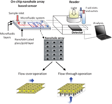 | ||
| Fig. 1 Schematic of the on-chip nanohole array based sensing concept. A nanofabricated gold-on-glass layer is integrated with a microfluidic system. The integrated chip has microfluidic components and optical access from both the top and the bottom. The sensor can be operated by transporting fluid over or through the nanoholes. The platform further includes an external interface comprising a reader unit with a light source, a detector and means for fluidic actuation and recording. | ||
In this review, advances in nanohole array based sensors integrated into microfluidic environments are surveyed. The perspective of this review accounts for the natural time progression along the development and implementation of nanohole arrays, their integration with microfluidic platforms and their relevance in sensing applications. With basis in the recent advancements in fabrication techniques and different operation methodologies, we review on-chip nanohole arrays operating in flow-over and flow-through modalities. Finally, we discuss current challenges and outline future opportunities for on-chip nanohole array based sensors.
2. Fabrication of nanohole array sensors
In general, several aspects influence the successful implementation of new technology, including materials and fabrication costs. As precious metals are commonly used in the fabrication of nanohole array plasmonic sensors, the associated materials cost is frequently a source of debate. Gold price, for instance, has markedly increased over the past decade, reaching the 1800 USD per troy ounce mark in 2011.45 This is around 57 USD per gram of gold. The amount of metal utilized in the fabrication of a nanohole array, however, is small. As an example, a nanohole array with a footprint of 10 by 10 microns, hosting about 400 nanoholes of 300 nm diameter with 500 nm spacing would occupy a volume of ∼7 × 10⁻¹⁸ m3. The cost of the gold required for this particular case would be around 10−8 USD. In other words, the cost of the gold required to fabricate ∼100 million nanohole array sensors is 1 USD, which is competitive compared to other sensing technologies.In the past two decades, several techniques for the fabrication of nanohole arrays have been reported. These techniques include both novel schemes and variations to already available practices. This review covers relevant techniques for the fabrication of (i) dead-ended nanohole arrays and (ii) through nanohole arrays. This classification is intended to provide a lucid contrast between the two different nanohole array operation modalities and to emphasize the advantages provided by modern methodologies. Dead-ended holes are used in a flow-over operation mode, in which the fluid containing the analyte is transported over the nanohole array. Through-hole nanoholes are used fundamentally as nanochannels, in a so-called flow-through modality, enabling the nanoconfinement of analyte inside the nanoholes. Fundamental differences between both approaches, from a fluidics perspective, are illustrated in Fig. 1 and discussed in detail in the following sections of this review. In general, nanofabrication techniques have been widely reported and reviewed in the past.46–50 A full coverage of nanofabrication methodologies has been recently covered in detail by Lindquist et al.,51 and is beyond the scope of this review. Here, we include techniques closely related to on-chip nanohole array based sensing. We focus on techniques that originally facilitated the fabrication of nanohole arrays, as well as techniques that advanced their optical attributes.
2.1 Focused ion beam
Focused ion beam (FIB) milling was first used to fabricate nanohole arrays in metal films.32 The FIB technique utilizes a beam of low energy ions to remove material from a sample by collision and is capable of achieving resolutions on the order of 10 nm.50,52,53 The most common source metal ion used in FIB milling is gallium, but Au–Si–Be and other alloys may also be used when lighter mass ions are required. FIB milling is a maskless, direct-writing technique in which the incursion depth of the ions can be finely tailored by adjusting the ion energy, facilitating the fabrication of multidimensional structures, including nanoholes.26,54–58 The mechanisms and parameter dependency of FIB milling involve two processes, sputtering and redeposition, and have been recently discussed by Zhou and Yang.57 During sputtering, high-energy ions remove material as they enter the substrate, reducing their momentum while doing so. The milling depth and volume may be estimated as a function of materials parameters and, importantly, the ion-beam current.57,59 During redeposition, the removed material from the substrate is either relocated onto the surface of the substrate or sputtered away. The redeposition volume may also be estimated in terms of ion beam and substrate parameters.52,57 With basis on the above two processes, the time required for FIB milling may be estimated as t = Vm/(Vs − Vr), where Vm is the total milled volume, Vs the sputtered volume rate and Vr the redeposition volume rate.57 These FIB milling parameters have been broadly assayed in the past in order to achieve nanohole arrays with excellent optical and mechanical attributes.26,30,34,37,41,60–70Fig. 2a shows a picture of nanoholes fabricated by FIB milling. Compared to other fabrication techniques, FIB milling requires specialized equipment and it is recurrently regarded as time consuming and less cost effective, especially when nanoholes are sequentially fabricated. Especially, FIB is not well-suited for mass-production. FIB, however, can be employed for a wide variety of materials, including metals and semiconductors; it can make use of mask patterning to fabricate entire nanohole arrays at once and, consequently, it is commonly used nowadays.64,70–73 Additionally, FIB can be employed in the fabrication of through nanoholes in free-standing gold-on-nitride films, which presents advantages in terms of sensing as discussed later in this work.43Fig. 2c shows an image sequence of the fabrication of a through nanohole using FIB. Milling through the 100 nm Au layer (t1 through t3) is relatively fast (<1 s) compared to milling through the nitride layer (∼3 s) as expected. Fig. 2b shows an SEM image of an array of through nanoholes fabricated via FIB from the nitride side.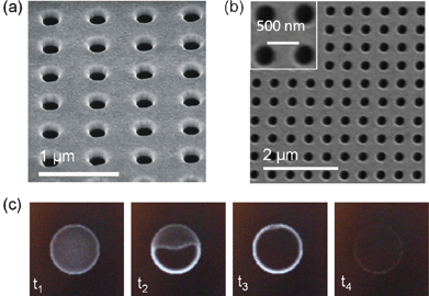 | ||
| Fig. 2 Nanohole arrays fabricated by focused ion beam lithography (FIB). (a) SEM image of an array of non-through nanoholes. This nanohole array was fabricated in a 100 nm thick film of gold supported by a glass substrate through a Ti–W adhesion layer. (b) SEM image of an array of through nanoholes. This nanohole array was fabricated through a 100 nm thick film of gold supported by a Si3N4 membrane of 100 nm thickness. (c) Image sequence of the fabrication of a nanohole through an Au-on-Si3N4 membrane. The time interval between the images is ∼0.2 s. | ||
2.2 Electron beam lithography based techniques
Another general technique employed in the fabrication of metallic nanohole arrays is electron beam lithography (EBL).40,69,74 EBL may have variations or may be combined with other fabrication procedures, such as chemical etching methods, depending on the desired final nanostructures. EBL is derived from scanning electron microscopy (SEM) and utilizes a focused beam of electrons to enable fabrication by either direct-writing or by lift-off procedures.75,76 The latter is a common practice with benefits in terms of versatility by employing a layer of either positive or negative tone photoresist. When using positive tone resist, for instance, the e-beam irradiated resin is chemically removed to develop the final structure. In most cases, EBL, as with lithographic techniques in general, involves three steps: coating a substrate with the photoresist, electron beam (e-beam) exposure and chemical development.57 The photoresist is spin-coated over a flat substrate, commonly glass, and soft-baked and subsequently patterned with nanostructure using an e-beam. Chemical development exposes the negative resist pattern on the substrate. The next step is metal deposition that can be achieved through intermediate metallic adhesive layers. A common procedure, for example, consists in the deposition of a thin layer of Cr (∼5 nm) followed by the deposition of a thicker layer of Au (∼100 nm). To obtain the Au nanohole array, the remaining photoresist layer (i.e. the sacrificial layer) is finally lifted off. Overall, EBL is well-suited for the high-yield nanohole fabrication of structures on the lower tens-of-nanometre scale.50,77 EBL then, is a highly versatile fabrication technique with the capability of using both positive and negative tone photoresists, and for fine-tailoring both the size and pitch of the nanoholes.2.3 Lift-off-free evaporation (LIFE) technique
A lift-off-free procedure, based on single layer e-beam lithography, reactive ion etching (RIE) and the deposition of metallic layers has been recently reported by Yanik et al.78 for the fabrication of free-standing nanohole arrays. A schematic representation of the nanofabrication of nanohole arrays with this approach is shown in Fig. 3a. In this technique, free-standing silicon nitride (SiNx) films are used as substrates. The films are produced by low pressure chemical vapour deposition of SiNx on a silicon wafer, and subsequent optical lithography and dry/wet etching. The nanohole array pattern is then created on spin-coated positive resist on the free-standing film by standard EBL, and subsequently extended to the nitride film using RIE. After the resist is removed using oxygen plasma, an Au film, with thickness on the order of 100 nm, is deposited via a thin Ti adhesive layer (∼5 nm) to reveal the final gold-on-nitride arrays of through holes. The nanohole arrays fabricated using LIFE had high-quality plasmonic resonances, with full width at half maximum (FWHM) of ∼20.78Fig. 3b and 3c show, respectively, a picture of the fabricated nanoholes and the optical response of LIFE-fabricated nanohole arrays to solutions of different refractive indices, as reported by Yanik et al.78 The bulk refractive index sensitivity of the nanohole arrays fabricated with this technique was 600 nm/RIU, which is markedly superior to sensitivities of nanohole arrays fabricated with other techniques29,30,34,37,43,50 and almost half of the highest reported previously.79 The reported figure of merit (FOM) for the nanohole arrays fabricated through the LIFE technique was ∼40.80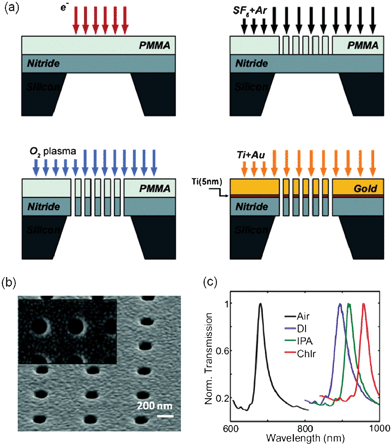 | ||
| Fig. 3 (a) Schematic of the LIFE fabrication technique. First, e-beam lithography is carried out on a PMMA-coated free-standing nitride membrane. A subsequent RIE process conveys the nanohole array outline to the nitride. The nanohole array is then extended through the nitride by oxygen plasma exposure. A final metal deposition step generates the Au nanohole array onto the nitride membrane; (b) SEM image of an array of through holes fabricated using the LIFE technique;80 adapted with permission from A. A. Yanik, M. Huang, O. Kamohara, A. Artar, T. W. Geisbert, J. H. Connor and H. Altug, Nano Letters, 2010, 10, 4962–4969. Copyright 2010 American Chemical Society; (c) resonance peaks of the transmitted light spectra from nanohole arrays fabricated using the LIFE technique, for different solutions with different indices of refraction: air, deionized water (DI, n = 1.333), isopropyl alcohol (IPA, n = 1.377) and chloroform (n = 1.49).78 Adapted with permission from A. A. Yanik, M. Huang, A. Artar, T. Y. Chang and H. Altug, Applied Physics Letters, 2010, 96, 021101. Copyright 2010 American Chemical Society. | ||
2.4 Nanoimprinting
Another technique utilized in the fabrication of nanohole arrays is based on imprinting a polymeric film with a mould.81–83 Nanoimprint lithography (NL) based techniques have been used in the fabrication of both dead-ended and free-standing (i.e. through) nanohole arrays. A negative mould of the nanostructures is used as a stamp to imprint the pattern on a layer of either thermoplastic or UV-curable material.50 After it is released, the mould leaves a reproduction of the nanostructures on the cured (or set) polymer which can then be coated by a metallic layer. In nanohole array based sensors, the metallic layer is commonly gold with a thickness of between 50 and 100 nm deposited via a thin adhesive Ti layer of a few nanometres.75,82,84 In the case of thermoplastic resists, NIL requires raising the temperature of the polymer above its glass transition temperature (Tg) prior to imprinting, and lowering the temperature below Tg after releasing the mould.84,85 As discussed by Guo,85 thermal expansion may limit the applicability and selection of materials for this technique. Therefore, temperature and pressure control play an important role in NIL. UV-curable materials are good candidates to evade these thermal effects. Most common UV-curable materials nowadays are based on free-radical polymerization of acrylic and methacrylic monomers.86 Nevertheless, these materials present drawbacks related to oxygen sensitivity and post-exposure shrinkage. Alternatives to these are UV-curable epoxysilicone materials,85 and other imprintable materials such as cyclic olefin copolymers,87 fluoropolymers88 and biodegradable polymers, such as poly-(L-lactic acid) (PLA), for applications requiring biocompatibility.89 Moulds can be fabricated using several materials including poly(dimethylsiloxane) (PDMS) and SiO2 and by different methods, such as the combination of EBL and RIE, for instance.81,82,84 NL is well-suited for large-area pattern fabrication and allows the fabrication of both free-standing and over-a-substrate nanohole arrays.50 In terms of cost, NL involves the use of specialized equipment and otherwise costly procedures for the creation of the moulds, such as e-beam and RIE. However, nanoimprint stamps can be enduring and may be reused repeatedly.81,852.5 Template stripping
A template stripping approach for the high-throughput fabrication of inexpensive Ag nanohole arrays has been recently reported by Im et al.90 This method combines template stripping and atomic layer deposition for the fabrication of nanohole arrays in Ag films with suitable thickness and optical properties, comparable to established techniques. The procedure is illustrated in Fig. 4.90 The prefabrication of a Si nanoimprint stamp is required prior to the actual fabrication of the metallic nanohole array. The stamp is used to imprint the nanohole array pattern on a thermal resist on a thermally oxidized Si wafer (Fig. 4a). RIE and deep reactive ion etching are then used to generate deep nanoholes in the Si wafer (Fig. 4b). A directional Ag deposition step forms the metallic nanohole arrays (Fig. 4c) which are subsequently coated with a UV-curable epoxy and covered by a glass slide. The epoxy is next cured and, as a final step, the metal–epoxy–glass assembly is next peeled off the Si template. The resulting metallic surface is notably smooth and, thus, of high optical quality for plasmonic sensing.90–92 This approach represents an excellent alternative for the inexpensive fabrication of nanohole arrays with substantial surface extension. A possible drawback of this technique is the use of Ag for microfluidic applications, due to the reduced biocompatibility and chemical stability. However, this issue has been effectively addressed by Im et al. through the deposition of thin layers of silica90 or alumina.93 The measured bulk refractive index sensitivity of template-stripped Ag nanohole arrays is ∼450 nm per refractive index unit (RIU), comparable to the sensitivity of nanoholes fabricated in Au with established fabrication techniques.26,43,90 By using Ag instead of Au, this approach presents a potential reduction of 50-fold in metal cost, in addition to the financially viable fabrication procedures associated with it. These benefits have exposed new opportunities for nanohole array based biosensors for real-world application in which robustness and cost-efficacy are compulsory.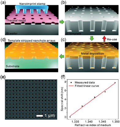 | ||
| Fig. 4 Schematic of the template-stripping method for the fabrication of large-area nanohole arrays. (a) A Si wafer is first coated with resist and subsequently imprinted with a stamp; (b) an etching step process produces a Si template with deep holes; (c) an Ag layer is deposited on the Si template; (d) an epoxy film is applied to the metal coating and then covered with a glass slide. The Ag film is then peeled off the template to reveal the smooth nanohole array made in the metal film; (e) SEM image of a template-stripped nanohole array; (f) measured bulk refractive index sensitivity of nanohole arrays fabricated by the template-stripped technique.90 Adapted with permission from H. Im, S. H. Lee, N. J. Wittenberg, T. W. Johnson, N. C. Lindquist, P. Nagpal, D. J. Norris and S.-H. Oh, ACS Nano, 2011, 5, 6244–6253. Copyright 2011 American Chemical Society. | ||
2.6 Soft interference lithography
Soft interference lithography (SIL) has been used to produce quasi-infinite arrays of free-standing metallic nanoholes with exceptional spectral qualities.94 SIL combines interference lithography (IL) and soft lithography (SL) techniques to produce optically smooth nanohole arrays over large areas. This technique was introduced by Henzie et al.94 in 2007. IL, reported elsewhere,95–98 is used to fabricate large-area, high-quality silicon masters with arrays of nanoposts with diameters and pitch matching those of the to-be fabricated nanoholes. The heights of the posts must satisfy the complete incursion of an elastomer, such as PDMS, in order to produce transparent photomasks: 400 nm in the procedure by Henzie et al.94 Notably, hundreds of defect-free elastomeric photomasks with the nanohole array pattern can be produced using a single IL master. The next step involves SL printing: the SIL PDMS photomask is then placed in close contact with a thin layer of photoresist on a Si wafer. A comprehensive review on SL techniques has been recently compiled by Lipomi et al.98 Finally, the photoresist pattern is transferred to a free-standing metal using phase-shifting photolithography, etching, e-beam deposition and lift-off (PEEL), which is a well-established soft nanofabrication technique, reported elsewhere.98–100 A possible challenge to large-area nanohole arrays on free-standing metal films would be the mechanical stability, especially in applications requiring fluid transport through the nanoholes (see flow-through operation in Fig. 1). However, the use of microstructured scaffolds, fabricated through established and straightforward methods, for instance, could be used to avoid the structural collapse of the metal film. Henzie et al. characterized large-area Au-on-glass nanohole arrays fabricated by SIL, including the zero-transmission resonance peak response to the change in the refractive index of different solutions.94 The arrays fabricated with SIL exhibited sensitivities of ∼300 nm/RIU which are similar to those of nanohole arrays fabricated using FIB, and the top FOM of 23.3, for patches (i.e. non-infinite arrays) of Au nanohole arrays.943. On-chip nanohole array based sensing
Whilst optics and microfluidics merged to produce a new field referred to as optofluidics,101 the combination of plasmonics and microfluidics has emerged as an area with unique attributes and explicit applicability, particularly, in bioengineering.28,67 Kim recently provided an elegant review on this new area,39 which he accurately identified as plasmo-fluidics. On-chip nanohole array based sensing technology participates in this new stream of technology, sharing challenges and opportunities. Achieving miniaturization of nanohole array based sensing technology at the individual device level requires integration of subwavelength optical components into microfluidic platforms. The development of such integrated systems has occurred over the past five years and has progressed rapidly. On-chip nanohole array sensing has rapidly evolved from single-array, single-channel arrangements to multiple arrays of nanohole arrays with complex fluidic structures for multiple and parallel analyte sampling. On-chip nanohole array based sensors have been operated in two fluidic modalities. Initial on-chip nanohole array based sensors were operated in flow-over sensing mode, in which the sample solution containing the analyte flows on top of the nanohole arrays.38 A flow-through sensing mode was later proposed, combining the characteristics of nanohole arrays for both fluidic transport and plasmonic sensing.43,102 In the following two sections, we will review recent advances in on-chip nanohole array based sensing, in the context of their fluidic operation modality.3.1 Flow-over sensing
Early experiments by Brolo et al. in 2004 demonstrated the potential of nanohole arrays as sensing elements.26 In these early experiments, nanohole arrays were used for the SPR label-free detection of the formation of a self-assembled monolayer and the successive adsorption of bovine serum albumin. In addition, these experiments also demonstrated key advantages over other SPR-based methodologies, including micrometre-scale footprints, simple optical equipment requirements and, notably, their compatibility with microfluidic schemes. The first on-chip integration of nanohole arrays came in 2007, when De Leebeeck et al. incorporated nanohole arrays within a microfluidic chip to detect sequential refractive index changes, spatial microfluidic concentration gradients and biochemical binding events.38 This platform, shown schematically in Fig. 5a, was formed of arrays of 150 nm diameter nanoholes fabricated via FIB milling, with square footprints in the order of 400 μm2, and periodicities ranging from 350 to 850 nm. The transmitted light spectra from the integrated platform in response to solutions with different refractive indices are shown in Fig. 5b. The bulk refractive index sensitivity was 333 nm/RIU, similar to established plasmonic technology reported previously. The device was capable of detecting a sucrose solution cross-stream concentration gradient and resolving the profile change of the concentration gradient in response to a change in the flow rate. As for the detection of biochemical binding events, the platform was used to monitor the sequential formation of a cysteamine–biotin–streptavidin complex, in similitude to bioanalytical practices. The average peak-shift from the transmitted spectra was ∼4 nm, as shown in Fig. 5c. This first set of experiments demonstrated the potential of on-chip nanohole array based sensing platforms, which prompted the exploration of new applications and the continuous innovation that this technology has seen up to now.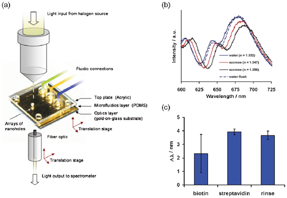 | ||
| Fig. 5 (a) Schematic of the on-chip nanohole array platform, detection scheme and fluidic access ports used by De Leebeeck et al.; (b) transmission spectra from the integrated platform in response to solutions with different indices of refraction; (c) relative spectral peak shift obtained from the sequential addition of biotin, streptavidin and PBS (rinsing).38 Adapted with permission from A. De Leebeeck, L. K. S. Kumar, V. de Lange, D. Sinton, R. Gordon and A. G. Brolo, Analytical Chemistry, 2007, 79, 4094–4100. Copyright 2007 American Chemical Society. | ||
During this early optofluidic integration stage, Pang et al. developed an analytical expression of sensitivity for two-dimensional nanohole array SPR sensors, based on morphological and plasmonic characteristics of the arrays.79 This expression was validated experimentally through the detection of near-surface refractive changes, and the real-time monitoring of anti-BSA binding to the BSA-functionalized surface of an Au nanohole array integrated with microfluidic delivery. The measured sensitivity for the (1, 0) surface plasmon polariton (SPP) mode reported from these experiments was 1520 nm/RIU, in close agreement with the 1526 nm/RIU value obtained from the analytical expression.
Whilst nanohole SPR based sensing has relied extensively on spectroscopy, the surface plasmon resonance imaging (SPRI) technique has played an important role in the advancement of on-chip nanohole array sensing technology as well.103–108 SPRI finds its roots in surface plasmon resonance microscopy (SPRM) used in conventional SPR techniques in the past,109–111 and has been used in many applications involving SPR and microfluidics.42,68,107,112–118 Along this avenue, Lesuffleur et al. demonstrated the possibility of achieving high-throughput SPRI by using on-chip nanohole array based sensors.41 In this approach, a 16 by 16 array of nanohole arrays with individual footprints of ∼30 μm2 was integrated into a microfluidic flow cell. The nanoholes were FIB-milled, 200 nm in diameter and had periodicities between 380 nm and 460 nm. The experimental setup, schematically illustrated in Fig. 6a, included a linearly polarized HeNe laser beam directly illuminating the on-chip plasmonic platform from the bottom. The light was acquired via a cooled CCD camera attached to an upright microscope. The use of collinear transmission imaging in this setup eluded the time-consuming optical alignment required in techniques reported previously.31,112,119,120 The nanohole arrays were enclosed in a microfluidic chip, using tubing for fluid delivery. A picture of the integrated on-chip nanohole array sensing platform is shown in Fig. 6a. The sensing response of this platform was evaluated through a standard detection protocol121 for monitoring the formation of a SAM from a 4 nm alkanethiolate solution. The measured time constant obtained from binding kinetics experiments using this platform was 56 min−1 and the detection sensitivity, measured as the ratio of the transmitted intensity change over the variation of the effective refractive index (IT/Δn),122 reached 16![[thin space (1/6-em)]](https://www.rsc.org/images/entities/char_2009.gif) 600%/RIU. With this sensitivity and a packing density estimated in the ball-park of 40k spots cm−2, this approach presented great promise for assisting DNA and protein microarray technologies. Notably, the combined experimental simplicity and nonparallel multiplexing capabilities of the technique presented by Lesuffleur et al. opened up new opportunities for on-chip nanohole array sensors to inaccessible fields at that time, such as proteomics, where high-throughput is a must. Concurrently, on-chip nanohole arrays were used in cell biology studies in similar high-throughput fashion. Also employing SPRI, Ji et al. achieved the simultaneous monitoring of glutathione S-transferase (GST) and anti-GST from multiple nanohole arrays.40 The on-chip platform consisted of 25 arrays of 150 nm-diameter nanoholes with individual footprints of 3.3 μm by 3.3 μm, spaced approximately 100 μm from each other, within a microfluidic encasement. The plasmonic nanostructures were fabricated by both FIB milling and direct-write EBL. Successful real-time monitoring of 25 biological binding events with millisecond-scale temporal resolution and an outstanding sensitivity of ∼10−7 RIU were achieved with this platform. Although only 25 nanohole arrays were studied in the experiments reported by Ji et al., this type of platform could afford shorter spacing between sensors. This would increase the density of nanohole arrays, to host up to approximately 20 thousand sensors on an area that can be resolved by CCD imaging techniques.
600%/RIU. With this sensitivity and a packing density estimated in the ball-park of 40k spots cm−2, this approach presented great promise for assisting DNA and protein microarray technologies. Notably, the combined experimental simplicity and nonparallel multiplexing capabilities of the technique presented by Lesuffleur et al. opened up new opportunities for on-chip nanohole array sensors to inaccessible fields at that time, such as proteomics, where high-throughput is a must. Concurrently, on-chip nanohole arrays were used in cell biology studies in similar high-throughput fashion. Also employing SPRI, Ji et al. achieved the simultaneous monitoring of glutathione S-transferase (GST) and anti-GST from multiple nanohole arrays.40 The on-chip platform consisted of 25 arrays of 150 nm-diameter nanoholes with individual footprints of 3.3 μm by 3.3 μm, spaced approximately 100 μm from each other, within a microfluidic encasement. The plasmonic nanostructures were fabricated by both FIB milling and direct-write EBL. Successful real-time monitoring of 25 biological binding events with millisecond-scale temporal resolution and an outstanding sensitivity of ∼10−7 RIU were achieved with this platform. Although only 25 nanohole arrays were studied in the experiments reported by Ji et al., this type of platform could afford shorter spacing between sensors. This would increase the density of nanohole arrays, to host up to approximately 20 thousand sensors on an area that can be resolved by CCD imaging techniques.
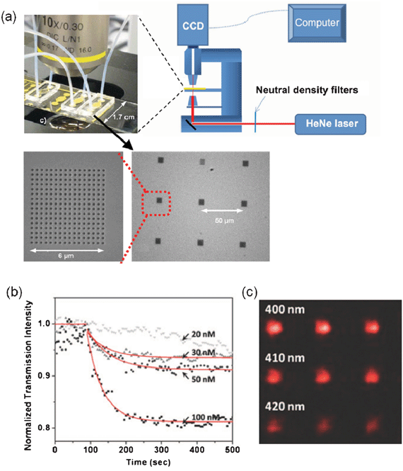 | ||
| Fig. 6 (a) Schematic of the experimental setup; picture of the integrated on-chip nanohole array platform; and SEM images of the nanohole array arrangement contained within the platform reported by Lesuffleur et al.41 Adapted with permission from A. Lesuffleur, H. Im, N. C. Lindquist, K. S. Lim and S. H. Oh, Optics Express, 2008, 16, 219–224. Copyright 2008 Optical Society of America; (b) real-time kinetics monitoring of streptavidin–biotin binding for different concentrations of streptavidin; (c) CCD image of the transmitted light from an array of 9 nanohole arrays illuminated with a HeNe laser.125 Adapted with permission from H. Im, A. Lesuffleur, N. C. Lindquist and S.-H. Oh, Analytical Chemistry, 2009, 81, 2854–2859. Copyright 2009 American Chemical Society. | ||
However, the relevance of on-chip nanohole array platforms had still to overcome important challenges in order to accomplish the forecasts. High-density packing, for instance, could be detrimental to the sensitivity and overall performance of the platforms due to plasmonic interference and cross talk between arrays.123 Additionally, reduction in the individual footprints of the arrays could also affect the quality of the transmission resonance peaks with similar detrimental effects.124 To overcome these challenges, Lindquist et al. demonstrated the use of supplementary plasmonic Bragg structures to overturn the SP waves from densely-packed nanohole arrays.68 The hybrid plasmonic structures were fabricated by FIB milling and consisted of square arrays of 3-by-3, 7-by-7 and 16-by-16 nanoholes of 150 nm in diameter, surrounded by 50 nm-deep and 100 nm-wide square grooves. The spacing between sensors was ∼3 μm. The use of these plasmonic mirrors facilitated the confinement of the transmitted light within the nanohole array area, resulting in sharper resonance peaks and increased sensitivity. The real-time monitoring of biotin–streptavidin was used to demonstrate multiplex sensing and to compare the performance between arrays of different sizes.
Im et al. integrated sets of nanohole arrays with different resonance wavelengths in individual microchannels and demonstrated multiplex SPR microarray imaging and differential sensing of binding kinetic events.125 The experimental sensing assessment used in this study was analogous to the above-mentioned approach by Lesuffleur et al.41 The microarray consisted of 252 sensing elements with a packing-density of 1.45 × 10⁶ arrays per cm2. The multichannel microarray format was used to monitor specific binding of streptavidin to biotin, including multiple negative controls in real-time, under microfluidic flow rates of ∼2 μl h−1. The limit of detection of the platform was investigated by monitoring the binding kinetics of biotin and streptavidin at different concentrations ranging between 20 nM and 100 nM, as shown in Fig. 6b. The lower limit value was the minimum concentration for obtaining a detectable signal and the measured affinity constant was ∼4 × 10⁶ M−1. Fig. 6c shows an actual transmission image from a 3 by 3 group of nanohole arrays during a SPRI demonstration by Im et al.125
Having demonstrated the multiplexing capabilities of integrated arrays of nanohole arrays in microfluidic networks, Im et al. took a step forward towards the development of affordable on-chip sensing platforms by employing large-area nanohole arrays fabricated via template stripping.90 This technique was first utilized to fabricate massive arrays of nanoholes made of Ag, which demonstrated not only competitive optical and on-chip biosensing performance, but also the potential for a substantial reduction in fabrication and materials costs. The same fabrication approach was subsequently used by Im et al. to generate on-chip sensing platforms with large-area nanohole arrays in Au for investigating a broad range of antibody–ligand binding kinetics in real-time with outstanding resolution.126 The sensing platform consisted of an integrated array of 200 nm-diameter nanoholes with 500 nm pitch in a PDMS microfluidic flow cell with external fluidic actuation. The system was accomplished using low-cost in-house fabrication procedures, a portable spectrometer and off-the-shelf optics. Using the valley around 720 nm from the transmission spectra, the platform achieved a bulk refractive index sensitivity of 481 nm/RIU. The extension of the nanohole array provided enough photon flux per pixel, which allowed for short acquisition times, low spectral noise and a resolution in the order of 10−6 RIU. The system was additionally used to investigate the binding kinetics of single-chain variable fragment (scFv) antibodies, as small as 25 kDa, to the protective antigen (PA) ligand of anthrax toxin. This platform, assembled from standard and off-the-shelf components, was able to resolve dissociation constants in a range of 200 pM to 40 nM, at concentrations as low as 1 nM.
Integration of optical and microfluidic components into compact and well integrated devices is important for the development of portable diagnostics.127 In an attempt to reach this level of portability and integration, Escobedo et al. reported an optofluidic hand-held SPRI sensing platform based on a dual-wavelength light source scheme. Fig. 7a and 7b show a picture of the system and a schematic of the sensing concept, respectively. The dual-wavelength light source was a two-color LED, used to increase the spectral diversity of the signal. The wavelengths were selected so as to respond in an opposite manner to SPRI sensing: the transmitted light intensity for one of them would increase while the second would decrease in response to bulk RI changes. This dual response is shown in Fig. 7c, for bulk RI changes using glucose solutions. The sensing attributes of the device were assessed by detecting aqueous ethanolic solutions with incremental ethanol content. The sensitivity and LOD of the device obtained from this test were 266 pixel intensity unit/RIU and 6 × 10⁻⁴ RIU, respectively. The platform was tested in the detection of dynamic surface binding events. An established biotin–streptavidin complex was selected for the test. Fig. 7d shows the biotin–streptavidin binding curve over time for one nanohole array of the platform. The response of the sensor showed the characteristic binding profile for this complex, reaching saturation after ∼40 min. It is important to note that the pixel intensity value was sustained after a final flush during the experiment due to the high affinity of the analyte complex. The integrated nature of this device, in combination with the availability and low cost of the components involved, holds great promise for point-of-care diagnostics and field research.
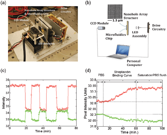 | ||
| Fig. 7 Hand-held on-chip nanohole array based sensing platform with a dual-wavelength light source. (a) Picture of the SPR sensing device indicating the different components; (b) schematic of the sensing device and picture of a nanohole array with a periodicity of 420 nm and hole diameters of 275 nm; (c) proof-of-concept dual-wavelength bulk refractive index sensing. The transmitted light intensity response is opposite for the 2 wavelengths used in the device; (d) real-time monitoring of biotin–streptavidin binding using the hand-held device with dual wavelength light source. The solution containing streptavidin is introduced at 10 min, and saturation is achieved after ∼40 min.58 Adapted with permission from C. Escobedo, S. Vincent, A. I. K. Choudhury, J. Campbell, A. G. Brolo, D. Sinton and R. Gordon, Journal of Micromechanics and Microengineering, 2011, 21, 115001. Copyright 2011 Institute of Physics (IOP). | ||
More recently, Tellez et al. demonstrated that bulk refractive-index resolution from on-chip nanohole array based sensors can be optimized by combining computational simulations with experimental procedures.128 This approach made use of numerical simulations to assay different architectural parameters of nanohole arrays, in order to find the operational ‘sweet spot’ wavelength. Experimentally, the sensitivity of the system was increased and the noise level lowered by adjusting operational parameters of the light source and the CCD detector. The combination of numerical simulations, experimental procedures and subsequent numerical filtering of the signal resulted in an unprecedented bulk resolution of ∼10−7 RIU.
The advancements and applications discussed above evidence the tremendous advancement that on-chip nanohole array based sensing has experienced in just a few years. In most of these applications, however, only the inherent optical properties of the nanostructures were exploited, failing to harness the benefits of nanoconfined fluidic transport combined with plasmonic sensing. In the following section, we will review the utilization of on-chip nanohole arrays in flow-through mode, in which the nanostructures are used not only as plasmonic sensors, but also as nanochannels.
3.2 Flow-through sensing
During the early developmental stage of on-chip nanohole array based sensors, the upper metallic surface of the nanoholes was assumed to provide most of the plasmonic signal. In 2009, however, a study by Ferreira et al. elucidated the role of the in-hole gold surface in the plasmonic response.63 In this study, the in-hole surface of nanohole arrays was addressed by blocking the upper gold surface with silicon oxide. The plasmonic response from top-blocked nanohole arrays was compared with conventional nanohole arrays with metallic upper surface exposed. The bulk refractive index sensitivity obtained with the top-blocked nanohole arrays was 650 nm/RIU, comparable to the sensitivity obtained with naked gold top arrays of ∼400 nm/RIU. These results suggested that the in-hole surface plays a dominant role in the peak shift employed in sensing. The findings from this work highlighted two noteworthy aspects from the on-chip nanohole array based sensing viewpoint: first, the limit of detection may be enhanced in nanohole based sensing by employing only the active in-hole surface; and second, effective transport of analytes to the in-hole surface is required. In other words, the potential benefits of exclusive in-hole plasmonic sensing would be possible by employing the nanoholes as nanochannels.37,129 This flow-through modality required the fabrication of nanohole arrays on free-standing substrates with enough mechanical strength to support fluidic transport across. Silicon nitride (S3N4) films were employed as the base substrate for fabricating arrays of through holes due to their excellent mechanical properties and their commercial availability. Previous studies on the mechanical performance of Si3N4 nanosieves130 and preliminary studies of nanohole array flow-through operation using transmission electron microscopy (TEM) nitrides102 also supported the use of this material. With the advent of a new flow-through modality, many other benefits were outlined: enhanced transport of reactants to the in-hole active area; rapid in-hole cross-stream diffusion of analytes; flow parallelization and solution sieving; high-efficiency utilization of analyte; and faster response during sensing.102,131The first demonstration of flow-through nanohole array based sensing was presented by Eftekhari et al. in 2009.43 The sensing platform consisted of arrays of through nanoholes fabricated by FIB lithography on TEM gold-on-nitride films, integrated into a microfluidic system. The integrated chip was interfaced with external pressure-control hardware to facilitate the delivery of fluid to the arrays from the nitride (i.e. bottom) side. Schematics of the experimental setup and a SEM image of the fabricated nanohole arrays are shown in Fig. 8. A preliminary flow-through test was conducted prior to the sensing experiments in order to prove fluidic transport through the nanoholes and to examine differences among arrays with different milling parameters. This test was achieved by visualizing a fluorescent dye streaming through the nanohole arrays while replacing aqueous solution at a flow rate of ∼5 μl min−1. The combination of milling parameters and nanohole dimensions allowed flow-through from three of the six arrays during this test, as shown in Fig. 8b. The visualization test was followed by SPR flow-through sensing for the detection of bulk RI changes using glucose solutions with fine refractive index gradations, which indicated a bulk RI sensitivity of 324 nm/RIU. The biosensing faculties of the novel flow-through approach were then evaluated through a performance comparison against analogous flow-over sensing schemes. To demonstrate sensing, the flow-through approach was first employed in monitoring the formation of a mercaptoundecanoic acid (MUA) monolayer in real-time. The detected adsorption indicated an observable surface adsorption constant (kobs) of 0.426 min−1, which denoted an enhancement compared to the rate in flow-over schemes reported previously.132 A second sensing experiment involved a one-on-one performance comparison of flow-through sensing versus an established flow-over scheme. The comparison was achieved by monitoring the spectral shift in response to RI changes from flowing different solutions through the systems at flow rates compatible with biosensing applications (∼1 μl min−1). The measured spectral shift from this experiment, shown in Fig. 8c, indicated a 6-fold enhancement in response time and a larger resonance shift when using the nanoholes as nanochannels. In the work by Eftekhari et al., the flow-through approach was finally used for detecting the sequential assembly of a dithiobis(succinimidyl) undecanoate (DSU) monolayer and subsequent adsorption of cancer biomarker PAX8 specific monoclonal antibody at a concentration of 80 nM. The results, shown in Fig. 8d, yielded a total spectral shift of ∼3 nm and observable adsorption rate constant of 0.455 min−1. Notably, the experiments by Eftekhari et al. introduced label-free surface-based detection with flow-through nanohole arrays and proved the viability of the technique towards biosensing applications.
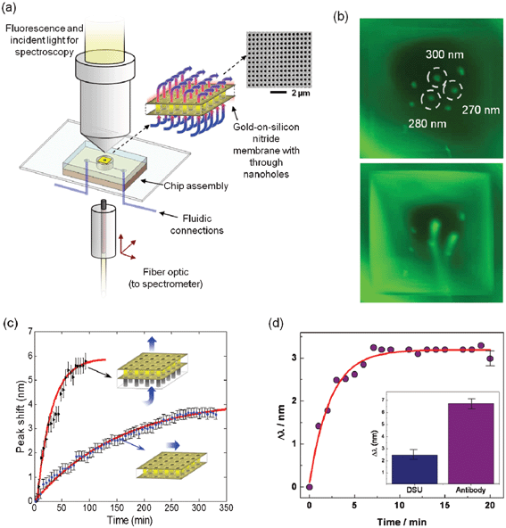 | ||
| Fig. 8 Flow-through nanohole array based sensing. (a) Schematic of the optical and fluidic test setup employed for both fluorescence tests and transmission spectroscopy; (b) fluorescence images of the gold film with nanohole arrays, before (top) and after (bottom) the application of fluid pressure. Arrays were 15 × 15 μm2, with periodicities of 450 nm and hole diameters of 300, 280, 270 nm (as indicated), as well as 260 and 250 nm. (Bottom) Fluorescence image showing a dye buffer solution streaming from the three largest diameter arrays with 70 kPa applied pressure; (c) comparison of response to surface adsorption achieved with flow-over and flow-through formats as indicated inset. Measured peak shift (625 nm peak) is plotted as a function of time during flow through/over of an ethanol/MUA solution. As indicated in the inset, the flow-through sensor is operated with flow from the non-participating silicon nitride side to the active gold surface; (d) response of flow-through nanohole arrays to sequential adsorption (periodicity of 450 nm). The wavelength versus time plot shows the peak-shift in response to the antibody (PAX8) adsorption, with a representative error bar on the last data point. Inset is a bar graph showing the peak shift in response to the initial DSU monolayer and the total peak shift in response to the DSU and the antibody.43 Adapted with permission from F. Eftekhari, C. Escobedo, J. Ferreira, X. Duan, E. M. Girotto, A. G. Brolo, R. Gordon and D. Sinton, Analytical Chemistry, 2009, 81, 4308–4311. Copyright 2009 American Chemical Society. | ||
A subsequent study by Yanik et al. confirmed the benefits of the nanohole array flow-through sensing approach.78 The through nanoholes in this case were fabricated on free standing silicon nitride using the LIFE technique and then coated with a 5 nm layer of Ti and a 125 nm layer of gold. The system consisted of a multilayered microfluidic structure accommodating the plasmonic structure. An arrangement of two inlets and two outlets at the upper and bottom layers of the microfluidic chip allowed full fluidic access to the nanohole array. Fluid delivery through the nanoholes was achieved by the combined blockage of one inlet and one outlet at opposite layers of the chip. The spectral shift measurements from replacing air with DI water under this targeted delivery of fluid through the nanohole array indicated a bulk RI sensitivity of 630 nm/RIU. A subsequent side-by-side comparison of the system operating in flow-over and flow-through modes indicated corresponding mass transport constants of 0.0158 min−1 and 0.2193 min−1, respectively. These results corresponded to a 14-fold improvement in mass transport and confirmed the potential of the hybrid platform for biosensing applications.
The benefits and applicability range of flow-through nanohole array sensing were studied in 2010 by Escobedo et al. through scaling analyses and computer simulations.133 In this study, the analyte sieving action, or collection efficiency, of a nanohole array operating in flow-through mode was quantified and contrasted with the flat sensor of an identical sensing surface under flow-over operation in a microchannel. For this comparison, rapid reaction kinetics at the sensing surfaces of both models was assumed in order to examine only mass transport effects. The collection efficiency was a function of the Péclet number (Pe), which determined the ratio of the total convective flux of molecules to the diffusive flux at the sensor as reported previously in the literature.134 From a scaling analysis, the flow-through nanohole array sensor demonstrated effective analyte collection (>99%) operating at an in-hole Pe ∼1 or below. In contrast, the corresponding flow-over scheme, with a Pe ∼102, achieved an analyte collection of only ∼2%. It is noteworthy that the Péclet number is not susceptible to changes in the dimensions in the microchannel containing the flow-over sensor. Therefore, the collection efficiency in such a case may only be improved by decreasing the flow rate by a factor of 300, at the cost of decreasing throughput and sensing response.
A computational model in this work offered a detailed transport analysis of the flow-through operation mode. The quantification of analyte flux as a function of the total flow rate from these simulations is shown in Fig. 9a. In this plot, the continuous line defines the limit for full collection134 and the dashed line indicates a mass transport asymptotic solution.135 For the specific comparison used in the scaling analysis, as indicated in Fig. 9a, the analyte flux in the flow-through format is 40-fold more than in the flow-over scheme. However, actual biosensors may operate in scenarios influenced not only by the mass transport but also by reaction kinetics at the sensing surface. The work presented by Escobedo et al. further examined the range of applicability of flow-through nanohole sensors as a function of analyte diffusivity and the characteristic timescale of the binding kinetics. Four analyte systems were considered: (1) a small molecule with favourable binding kinetics; (2) a system with similar characteristics to cancer biomarker CA125; (3) a small molecule with fast “on” kinetics; and (4) a small molecule with slow “on” kinetics. The gains of the flow-through format were important for systems (1) and (2), demonstrating much faster response time than the flow-over case. However, only a modest benefit was found for systems (3) and (4), due to the small molecular size of the analyte, which increases diffusive transport in both formats, and the intrinsic rate-limiting nature of the systems. Additional simulations quantified the improvement ratio of the flow-through scheme as compared to the flow-over format, as a function of the characteristic binding time scale. The simulations accounted for time scales spanning 5 orders of magnitude and “on-dominated” kinetics with adsorption constants ranging between 102 and 107 M−1 s−1 at a flow rate of 2 μl min−1. Each case was simulated for three different analyte diffusivities in order to account for different molecular sizes. The simulation results are shown in Fig. 9b. From these results, the benefit for small molecules and “slower” binding kinetics was evident, achieving values of up to ∼20-fold. Particularly, for binding time constants compatible with many biosensing applications, these results suggested a benefit of ∼10- to 20-fold in response time for flow-through nanohole array sensors. Significantly, this work studied not only the benefits, but also the limitations of flow-through nanohole array sensors.
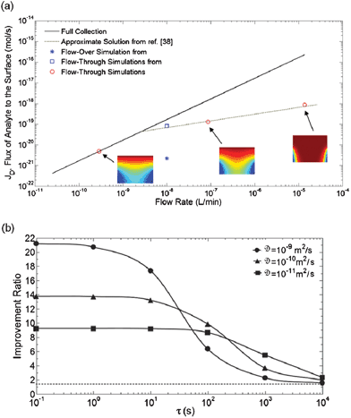 | ||
| Fig. 9 Computational simulations from the comparative analysis of transport in flow-over and flow-through sensing formats. (a) Total molecular flux to the sensing surface versus flow rate. The continuous line indicates the limit for perfect transport of analyte. The dashed line represents the flux estimated using the solution for mass transfer to a two-dimensional sensor as given by Ackerberg et al.135 Values corresponding to microchannel and nanohole cases are plotted, as indicated as in the legend, and additional sample flow-through computational results are shown inset.133 Adapted with permission from C. Escobedo, A. G. Brolo, R. Gordon and D. Sinton, Analytical Chemistry, 2010, 82, 10015–10020. Copyright 2010 American Chemical Society. | ||
Early work on flow-through nanohole array based sensing was soon followed by remarkable demonstrations of the biosensing capabilities of the optofluidic platform. The possibility to functionalize the sensitive in-hole surfaces of the nanoholes, in combination with their reputable near-surface sensing resolution, made them ideal candidates for the detection of antigen–antibody reactions and the recognition of immunoglobulin-based events. The factual significance of these benefits was consolidated by employing the optofluidic flow-through scheme for the direct detection of viruses.80 The strategy used by Yanik et al. in this work, involved the functionalization of flow-through nanohole arrays with antiviral immunoglobulins with common affinity for glycoproteins (GPs) from viruses of interest: vesicular stomatitis virus (8G5), PT-Ebola virus (M-DA01-A5) and Vaccinia virus (A33L). With this approach, GPs on the viral envelope from intact viruses would bind specifically at those segments of the sensor functionalized with antiviral antibodies, as illustrated in Fig. 10a. The platform included a total of 12 arrays operating in parallel, from which three were used as reference sensors. All nanohole arrays were fabricated using the LIFE technique and achieved outstanding optical attributes, with FOM values of ∼40. The platform exhibited a dynamic range spanning three orders of magnitude, high reproducibility and the ability to detect the viruses at low concentrations. Fig. 10b shows the spectral shifts obtained during the direct detection of Ebola and Vaccinia viruses at a concentration of 106 PFU mL−1. This platform could be extrapolated to multiplexed formats in which different pathogens contained in a common sample could be selectively recognized.
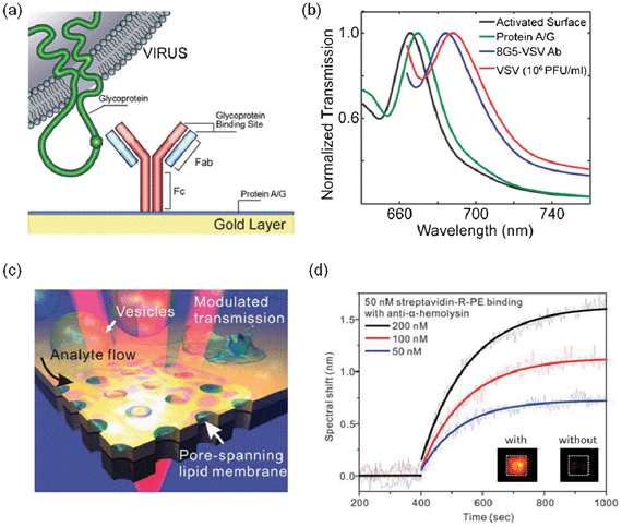 | ||
| Fig. 10 On-chip nanohole array based biosensing of viruses and toxins. (a) Schematic of the surface functionalization of the immunosensor reported by Yanik et al.80 for the detection of live viruses; (b) spectral shift obtained during the detection of intact viruses at concentrations of the order of 106 PFU mL−1.80 Adapted with permission from A. A. Yanik, M. Huang, O. Kamohara, A. Artar, T. W. Geisbert, J. H. Connor and H. Altug, Nano Letters, 2010, 10, 4962–4969. Copyright 2010 American Chemical Society; (c) schematic of the concept of a nanohole array sensor in free-standing gold-on-nitride films. The platform was used for sensing in a suspended lipid membrane environment through pore-spanning regions of the membrane, in analogy to biological membranes; (d) real-time kinetics measurements for 50 nM streptavidin labeled with R-Phycoerythrin (R-PE). The different curves correspond to the different concentrations of anti-α-HL antibodies. The insets show fluorescent images after binding of 50 nM streptavidin-R-PE with 100 nM anti-α-HL and to a negative control without α-HL.147 Adapted with permission from H. Im, N. J. Wittenberg, A. Lesuffleur, N. C. Lindquist and S.-H. Oh, Chemical Science, 2010, 1, 688–696. Copyright 2010 the Royal Society of Chemistry. | ||
In many cases, not the direct recognition of pathogens, but the detection of toxins secreted by these is required.136,137 Exotoxins, for instance, are microbial proteins secreted by certain types of pathogenic bacteria that promote disease. These proteins can diffuse away from the bacterium from which they are secreted.138 Lipid bilayer membranes play a central role in the study of the physiology of many of these diseases and drug therapies, as microbial toxins first interact with target cells through surface receptors.139 For instance, over half of the approved therapeutic drugs available nowadays target membrane proteins.140 Therefore, direct interrogation of biological events involving membrane-bound proteins is essential in drug discovery and biology research. Several studies have demonstrated the efficacy of microfluidic technology for toxin detection and screening.141–144 While immunochemistry detection has been most commonly achieved with these platforms,142,145 surface plasmon resonance methods have come into play as well.146 Im et al. reported a SPR biosensing approach based on the integration of arrays of through nanoholes with pore-spanning lipid membranes.147 An illustration of this biosensing approach is shown in Fig. 10c. This configuration allowed fluid access to the lipid membrane from the open surface at the top, and from nanoapertures at the bottom, facilitating the incorporation of transmembrane proteins into the pore-spanning regions of the membrane. The lipid membranes, formed by vesicle rupture,148 were used to modulate the plasmonic signal from the nanohole arrays. The platform was used in the detection of α-hemolysin (α-HL), a cytotoxic protein secreted by Staphylococcus aureus that binds to the membrane of mammalian cells.149 The shifts of the minima from the transmitted spectra were used for sensing. Sequential red-shifts in the transmitted spectra indicated the following successive events: formation of the lipid membrane, the incorporation of α-HL into the lipid membrane and binding of anti-α-HL to α-HL. Fig. 10d shows the spectral shifts from this biosensing experiment. The platform was also used to perform real-time kinetic assays of the binding events using anti-α-HL concentrations ranging between 50 nM and 200 nM. The measured dissociation constant and LOD from these assays were 1.9 × 10⁻⁸ M and 26 nM, respectively. In addition to the demonstrated biosensing capabilities, the platform presented by Im et al. offers minimum physical interaction with the lipid membrane and compatibility with cell plasma membranes.
The low concentrations at which many biomarkers in clinical samples are available represent a common challenge for sensing technology.150–152 In many cases, the concentration of an analyte may lie beyond the LOD of the sensing platform in question. In order to overcome this limitation, many on-chip sensing platforms have incorporated analyte concentration stages prior to sensing.153–155 Among other techniques, electric field gradient focusing (EFGF) has been employed for the concentration of electrically-charged analytes in microfluidic systems.156 With this technique, analyte enrichment is achieved by means of the non-uniform electric field distribution caused by the presence of a floating electrode embedded in the microfluidic system. Flow-through nanohole array sensors are capable of concentrating analyte by EFGF by using the metallic layer hosting the nanoholes as an electrode. The ability of flow-through nanohole arrays to perform as analyte concentrators and SPR sensors was introduced by Escobedo et al. in a recent study.44 In this work, EFGF was combined with an external pressure bias applied to the fluid in order to bring a concentrated plug of analyte into the nanoholes for sensing, as illustrated in Fig. 11a. This technique was employed first in a proof-of-concept experiment to concentrate fluorescein. An external electric potential of 50 V and a pressure bias of 4 kPa were used during this test. Fig. 11b shows the fluorescence image sequence obtained during the concentration process, as observed from the top (i.e. gold) of the nanohole arrays. The radial concentration profile observed was a consequence of the microfluidic architecture. The concentration process was repeated and observed from the bottom (i.e. nitride) side of the nanohole arrays. This second perspective demonstrated the evolution of the local fluorescence signal collected from each array and the lack of analyte streaming, suggesting the presence of concentrated analyte within the nanoholes. Fig. 11c is a plot of the concentration factor calculated from one of the nanohole arrays, reaching a value of ∼180-fold in one minute. The platform was then employed for the concentration and label-free sensing of bovine serum albumin (BSA) in order to extend its applicability to biomolecules. The surface of the sensor was functionalized with a DSU monolayer prior to experiments. Detection was achieved through SPR spectral shift measurements corresponding to BSA binding to the DSU monolayer, contrasting the rate of biomolecular binding with and without (i.e. control) the concentration process. From this study, the time required to reach equilibrium using the concentration approach was 10-fold faster than the control. Also, the magnitude of the peak-shift in the transmitted spectrum was 5-fold more under the concentration scheme. A computational model of the BSA concentration experiment, combining mass transport and first-order binding kinetics, predicted an enrichment of ∼100-fold. This optofluidic concentration demonstration opened up new possibilities for flow-through nanohole arrays to be operated beyond their intrinsic optical capacities.
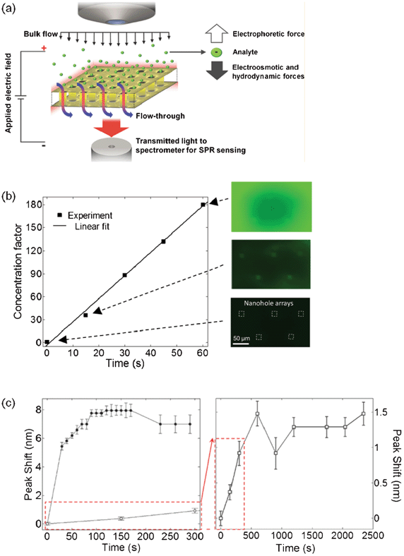 | ||
| Fig. 11 Optofluidic concentration. (a) Schematic of the concept. A through nanohole array in a metallic film embedded in a buffer induces a non-homogenous strength distribution of an externally applied electric field. Larger charged analytes respond to the locally increased field and concentrate. A pressure bias brings an enriched plug of analyte into the nanoholes for sensing; (b) optofluidic concentration of fluorescein over time from one nanohole array (top left from inset). The fluorescence images (right) show the changes in fluorescence intensity during the concentration process (50 V and 4 kPa applied); (c) resonance peak-shift monitoring of BSA binding to DSU under both active concentration (left; 50 V, 4 kPa) and control conditions (right; no applied field). With the applied field, the peak-shift reached a plateau after ∼120 s. The control experiment shows a slower binding rate without reaching saturation within the time range in this figure.44 Adapted with permission from C. Escobedo, A. G. Brolo, R. Gordon and D. Sinton, Nano Letters, 2012, 12, 1592–1596. Copyright 2012 American Chemical Society. | ||
4. Conclusions and future opportunities
The fusion of nanohole array based plasmonic sensing with microfluidics has made possible the development of integrated platforms with unique abilities. These faculties have been enabled not only by integration, but also by advances in nanohole array fabrication practices. The emergence of new techniques and the continuous adaptation of established methodologies have led to nanohole arrays with improved FOM and resolution, with reported values as high as 4078 and 10−7 RIU,128 respectively. These figures correspond to an increase of more than double for FOM and over 3-fold in resolution in just a few years. Also, massive arrays of nanoholes with footprints of the order of centimetres have been fabricated with lower-cost methodologies,126 facilitating the incorporation of multiple microfluidic structures onto a single nanoplasmonic structure. Particularly, the combination of nanoimprint lithography and template stripping has been demonstrated as an exceptional alternative for fabricating smooth large-area Ag nanohole arrays with high-throughput production scalability potential.90On-chip nanohole array based sensing has made use of both spectroscopic and imaging methods for sensing. The former exploited spectral-shift measurements from the transmitted light spectrum, while the latter utilized intensity variations from transmitted monochromatic beams. Both methodologies have been used to demonstrate label-free multiplex sensing with on-chip nanohole arrays.40–42,91
The introduction of flow-through nanohole array based sensing awarded these platforms with the benefits of exclusive in-hole sensing.43 By employing the nanoholes as nanochannels, on-chip nanohole array sensors demonstrated enhanced response times of up to 14-fold78 and the potential to extend this value to ∼20-fold.133 The biosensing capabilities of the flow-through format have been proved through the detection of relevant biomarkers43 and viruses.80
Overall, the performance demonstrations and applications surveyed throughout this work evidence the remarkable progress that on-chip nanohole array based sensing has experienced during the past decade. The combined reduction in fabrication costs, added functionality and improved performance may allow the dissemination of nanohole array based sensing in the future, as briefly outlined in the next sections.
4.1 On-chip nanohole arrays for cell studies
The surface extension of nanohole arrays may be designed to be compatible with the length scales of many cell types. For instance, nanohole arrays with footprints in the range of 5 to 30 μm, which encloses the average size of many mammalian cells, have been employed in the past for sensing.38,40,43,68 This length scale compatibility would allow the direct interrogation of single cells through individual nanohole arrays. The study of specific signal transduction pathways and genetic regulatory circuits in cancer cells reacting to biomechanical forces,157 for instance, could be achieved by addressing individual cells adhered to functionalized nanohole arrays. Additional opportunities concerning biomechanical forces from single cells may include studies on haematopoiesis during embryogenesis158 and mechanobiology.159,160 The three-dimensional compartmentalization of cells and targeted transport of media required in these cases may be achieved by microfluidics within the same optofluidic platform. This approach may assist, for example, in the elucidation of cell behaviour differences observed in genetically identical cells.161,162 The in situ investigation of binding kinetics from cellular membranes of living cells may also be possible by depositing or culturing cells in direct contact with the plasmonic structures.147,163From a fluidic viewpoint, the use of through nanoholes offers the possibility to assay cytotoxicity at the single-cell level by employing the microfluidic component of the integrated system to deliver different concentrations of a toxic agent, or therapeutic drug, through the nanoholes. Single or multiple arrays could be embedded into separate microfluidic channels to enable real-time monitoring of the course of cells contained within. At the same time, control assays could test for apoptosis and necrosis in separate regions of the platform. On this same avenue, it is worth mentioning that the study of apoptosis in microfluidic systems, alone, has been a matter of intensive research in the past few years.164–168 Apoptosis is characterized by a change in the refractive index of the cytoplasm and the plasma membrane and is thus suitable for nanohole array based SPR sensing.169 Some cell studies require the investigation of intracellular content through the partial or complete disruption (i.e. lysis) of the cellular membrane.170 The injection of lytic agents, as well as the controlled release of intracellular content may also be possible using the fluidic capabilities of nanohole arrays.
4.2 Active flow-through nanohole arrays
In addition to their inherent optical attributes used in plasmonic sensing, flow-through nanohole arrays offer the possibility to function as active elements. The possibility to use these optofluidic platforms to actuate their surroundings or to undertake dynamic morphological changes presents avenues for further exploration. The underlying mechanisms of optofluidic concentration, for example, are possible due to the presence and nature of the metallic nanostructures.44 This concept could be extended, for instance, to a ‘flow-through switch’, in which analyte with defined electrical properties is concentrated at one side of the nanohole array and then transported through it by changing the polarity of the applied field. In addition, optofluidic concentration is also applicable to additional sensing methods involving pores in a metal film, such as zero mode waveguides171,172 and nanopore-based single-molecule detection.173 Further opportunities may include the utilization of the mechanical properties of the substrates in which the nanohole arrays are fabricated. Development of tunable nanohole arrays on elastic free-standing substrates, for example, would enable morphological changes on the nanostructures by deflecting, or contracting, the substrate.4.3 Portable on-chip nanohole array based sensing platforms
The inherent small-scales of on-chip nanohole array based sensors are highly compatible for applications demanding portability, such as point-of-use diagnostics and remote health monitoring. The autonomy level required to achieve true portability requires the integration of the sensing platform and peripheral instrumentation into a single portable device. The device would be required to perform complete routines, including sample introduction and pretreatment, calibration and sensing per se. A recent attempt to achieve this level of integration utilized off-the-shelf components and straightforward circuitry to control LEDs as light sources and a CCD camera as detector.58 However, transport of fluids into and within the optofluidic sensor was achieved by external pumps. Self-sufficient fluidic actuation may be possible by straightforward ‘human-powered’ schemes, such as finger-powered microfluidic pumps,174 and unidirectional single-use schemes used currently in leading microfluidic diagnostics.175 With respect to light sources, light-emitting diodes (LEDs) have been used in integrated optofluidic platforms,58,176 and are excellent candidates as they are commercially available in a wide range of wavelengths and powers, and dimensions down to the sub-millimetre scale. The additional use of telecommunications technology would make possible the use of portable nanohole array based sensors in applications such as remote health monitoring, where the transmission of analysis results to centralized telehealth centres is required.Acknowledgements
The author gratefully acknowledges financial support from the Natural Sciences and Engineering Research Council of Canada (NSERC) postdoctoral fellowship program and ETH Zurich.References
- A. Manz, N. Graber and H. M. Widmer, Sens. Actuators, B, 1990, 1, 244–248 CrossRef.
- D. R. Meldrum and M. R. Holl, Science, 2002, 297, 1197–1198 CrossRef CAS.
- E. Delamarche, D. Juncker and H. Schmid, Adv. Mater., 2005, 17, 2911–2933 CrossRef CAS.
- G. M. Whitesides, Nature, 2006, 442, 368–373 CrossRef CAS.
- S. L. S. Freire and A. R. Wheeler, Lab Chip, 2006, 6, 1415–1423 RSC.
- S. Haeberle and R. Zengerle, Lab Chip, 2007, 7, 1094–1110 RSC.
- M. Mirzaei, M. Pla-Roca, R. Safavieh, E. Nazarova, M. Safavieh, H. Li, J. Vogel and D. Juncker, Lab Chip, 2010, 10, 2449–2457 RSC.
- A. K. White, M. VanInsberghe, O. I. Petriv, M. Hamidi, D. Sikorski, M. A. Marra, J. Piret, S. Aparicio and C. L. Hansen, Proc. Natl. Acad. Sci. U. S. A., 2011, 108, 13999–14004 CrossRef CAS.
- M. Unger, H. Chaou, T. Thorsen, A. Scherer and S. Quake, Science, 2000, 288, 113 CrossRef CAS.
- N. Polson and M. Hayes, Anal. Chem., 2001, 73, 312 A CrossRef CAS.
- D. Figeys and D. Pinto, Anal. Chem., 2000, 72A, 330 Search PubMed.
- A. J. Tudos, G. A. J. Besselink and R. B. M. Schasfoort, Lab Chip, 2001, 1, 83–95 RSC.
- E. T. Lagally, C. A. Emrich and R. A. Mathies, Lab Chip, 2001, 1, 102–107 RSC.
- M. A. Schwarz and P. C. Hauser, Lab Chip, 2001, 1, 1–6 RSC.
- T. Thorsen, S. J. Maerkl and S. R. Quake, Science, 2002, 298, 580–584 CrossRef CAS.
- H. Craighead, Nature, 2006, 442, 387–393 CrossRef CAS.
- S. Balslev, A. M. Jorgensen, B. Bilenberg, K. B. Mogensen, D. Snakenborg, O. Geschke, J. P. Kutter and A. Kristensen, Lab Chip, 2006, 6, 213–217 RSC.
- Nanotechnology Now, 2012, Nanotechnology in Drug Delivery: Global Markets, web 29 January 2012 Search PubMed.
- OSEC Business Reports, 2011, The Canadian Medical Technology Sector. Opportunities for Swiss Companies, OSEC Business Network Switzerland, web 3 March 2011 Search PubMed.
- C. H. Ahn, J. W. Choi, G. Beaucage, J. H. Nevin, J. B. Lee, A. Puntambekar and J. Y. Lee, Proc. IEEE, 2004, 92, 154 CrossRef CAS.
- M. Herrmann, T. Veres and M. Tabrizian, Lab Chip, 2006, 6, 555–560 RSC.
- S. K. Sia and L. J. Kricka, Lab Chip, 2008, 8, 1982–1983 RSC.
- C. D. Chin, V. Linder and S. K. Sia, Lab Chip, 2007, 7, 41–57 RSC.
- C. A. Baker, C. T. Duong, A. Grimley and M. G. Roper, Bioanalysis, 2009, 1, 967–975 CrossRef CAS.
- K. B. Mogensen and J. P. Kutter, Electrophoresis, 2009, 30, 200900101 CrossRef.
- A. G. Brolo, R. Gordon, B. Leathem and K. L. Kavanagh, Langmuir, 2004, 20, 4813–4815 CrossRef CAS.
- X. N. Shan, K. J. Foley and N. J. Tao, Appl. Phys. Lett., 2008, 92, 3 Search PubMed.
- J. N. Anker, W. P. Hall, O. Lyandres, N. C. Shah, J. Zhao and R. P. Van Duyne, Nat. Mater., 2008, 7, 442–453 CrossRef CAS.
- R. Gordon, D. Sinton, K. L. Kavanagh and A. G. Brolo, Acc. Chem. Res., 2008, 41, 1049–1057 CrossRef CAS.
- A. Lesuffleur, H. Im, N. C. Lindquist and S. H. Oh, Appl. Phys. Lett., 2007, 90, 243110 CrossRef.
- J. Homola, S. S. Yee and G. Gauglitz, Sens. Actuators, B, 1999, 54, 3–15 CrossRef.
- T. W. Ebbesen, H. J. Lezec, H. F. Ghaemi, T. Thio and P. A. Wolff, Nature, 1998, 391, 667–669 CrossRef CAS.
- C. Genet and T. W. Ebbesen, Nature, 2007, 445, 39–46 CrossRef CAS.
- P. Marthandam, A. G. Brolo, D. Sinton, K. L. Kavanagh, M. G. Moffitt and R. Gordon, Int. J. Nanotechnol., 2008, 5, 1058–1081 CrossRef CAS.
- Y. Iwasaki, T. Horiuchi and O. Niwa, Anal. Chem., 2001, 73, 1595–1598 CrossRef CAS.
- A. G. Brolo, Nat. Photonics, 2012, 6, 709–713 CrossRef CAS.
- D. Sinton, R. Gordon and A. G. Brolo, Microfluid. Nanofluid., 2008, 4, 107–116 CrossRef CAS.
- A. De Leebeeck, L. K. S. Kumar, V. de Lange, D. Sinton, R. Gordon and A. G. Brolo, Anal. Chem., 2007, 79, 4094–4100 CrossRef CAS.
- J. Kim, Lab Chip, 2012, 12, 3611–3623 RSC.
- J. Ji, J. G. O'Connell, D. J. D. Carter and D. N. Larson, Anal. Chem., 2008, 80, 2491–2498 CrossRef CAS.
- A. Lesuffleur, H. Im, N. C. Lindquist, K. S. Lim and S. H. Oh, Opt. Express, 2008, 16, 219–224 CrossRef CAS.
- T.-Y. Chang, M. Huang, A. A. Yanik, H.-Y. Tsai, P. Shi, S. Aksu, M. F. Yanik and H. Altug, Lab Chip, 2011, 11, 3596–3602 RSC.
- F. Eftekhari, C. Escobedo, J. Ferreira, X. Duan, E. M. Girotto, A. G. Brolo, R. Gordon and D. Sinton, Anal. Chem., 2009, 81, 4308–4311 CrossRef CAS.
- C. Escobedo, A. G. Brolo, R. Gordon and D. Sinton, Nano Lett., 2012, 12, 1592–1596 CrossRef CAS.
- The Economist online, 2011, Gold and the Swiss Franc. Flight to Safety, The Economist, web 20 July 2011 Search PubMed.
- B. D. Gates, Q. B. Xu, J. C. Love, D. B. Wolfe and G. M. Whitesides, Annu. Rev. Mater. Res., 2004, 34, 339–372 CrossRef CAS.
- G. M. Whitesides, B. Gates, Q. Xu, R. Boulatov, C. Love and D. B. Wolfe, Abstr. Pap. Am. Chem. Soc., 2004, 227, U514–U514 Search PubMed.
- G. M. Whitesides, B. Gates, B. Mayers and Q. B. Xu, Abstr. Pap. Am. Chem. Soc., 2005, 229, U936–U936 Search PubMed.
- B. D. Gates, Q. B. Xu, M. Stewart, D. Ryan, C. G. Willson and G. M. Whitesides, Chem. Rev., 2005, 105, 1171–1196 CrossRef CAS.
- M. E. Stewart, C. R. Anderton, L. B. Thompson, J. Maria, S. K. Gray, J. A. Rogers and R. G. Nuzzo, Chem. Rev., 2008, 108, 494–521 CrossRef CAS.
- N. C. Lindquist, P. Nagpal, K. M. McPeak, D. J. Norris and S.-H. Oh, Rep. Prog. Phys., 2012, 75, 036501 CrossRef.
- R. E. J. Watkins, P. Rockett, S. Thoms, R. Clampitt and R. Syms, Vacuum, 1986, 36, 961–967 CrossRef CAS.
- T. Ishitani and T. Ohnishi, J. Vac. Sci. Technol., A, 1991, 9, 3084–3089 CAS.
- Y. Fu, B. K. A. Ngoi, W. Zhou and T. F. Loh, Int. J. Nanosci., 2006, 5, 529–534 CrossRef CAS.
- T. Ohno, J. A. Bain and T. E. Schlesinger, J. Appl. Phys., 2007, 101, 083107 CrossRef.
- C. K. Chang, D. Z. Lin, C. S. Yeh, C. K. Lee, Y. C. Chang, M. W. Lin, J. T. Yeh and J. M. Liu, Appl. Phys. Lett., 2007, 90, 61113 CrossRef.
- J. Zhou and G. Yang, J. Manuf. Sci. Eng., 2010, 132, 011005 CrossRef.
- C. Escobedo, S. Vincent, A. I. K. Choudhury, J. Campbell, A. G. Brolo, D. Sinton and R. Gordon, J. Micromech. Microeng., 2011, 21, 115001 CrossRef.
- F. Itoh, A. Shimase and S. Haraichi, J. Electrochem. Soc., 1990, 137, 983–988 CrossRef.
- L. Yin, V. K. Vlasko-Vlasov, A. Rydh, J. Pearson, U. Welp, S. H. Chang, S. K. Gray, G. C. Schatz, D. B. Brown and C. W. Kimball, Appl. Phys. Lett., 2004, 85, 467–469 CrossRef CAS.
- J. C. Sharpe, J. S. Mitchell, L. Lin, H. Sedoglavich and R. J. Blaikie, Anal. Chem., 2008, 80, 2244–2249 CrossRef CAS.
- F. Eftekhari, R. Gordon, J. Ferreira, A. G. Brolo and D. Sinton, Appl. Phys. Lett., 2008, 92, 253103 CrossRef.
- J. Ferreira, M. J. L. Santos, M. M. Rahman, A. G. Brolo, R. Gordon, D. Sinton and E. M. Girotto, J. Am. Chem. Soc., 2009, 131, 436–437 CrossRef CAS.
- N. Huy, F. Sidiroglou, S. F. Collins, G. W. Baxter, A. Roberts and T. J. Davis, in Third Asia Pacific Optical Sensors Conference, ed. J. Canning and G. D. Peng, 2012, vol. 8351, p. 835128 Search PubMed.
- S. L. Yue and C. Z. Gu, 2007 7th IEEE Conference on Nanotechnology, vol. 1–3, 2007, 632–635 Search PubMed.
- L. A. Giannuzzi and F. A. Stevie, Introduction to Focused Ion Beams: Instrumentation, Theory, Techniques and Practice, Springer, New York, 2005 Search PubMed.
- A. G. Brolo, J. Ferreira, M. J. L. Santos, C. Escobedo, D. Sinton, E. M. Girotto, F. Eftekhari and R. Gordon, in Biosensing, ed. M. Razeghi and H. Mohseni, SPIE – the International Society for Optical Engineering, Bellingham, 2008, vol. 7035, p. 3503 Search PubMed.
- N. C. Lindquist, A. Lesuffleur, H. Im and S. H. Oh, Lab Chip, 2009, 9, 382–387 RSC.
- J. F. Masson, M. P. Murray-Methot and L. S. Live, Analyst, 2010, 135, 1483–1489 RSC.
- T. Sannomiya, O. Scholder, K. Jefimovs, C. Hafner and A. B. Dahlin, Small, 2011, 7, 1653–1663 CrossRef CAS.
- A. P. Blanchard-Dionne, L. Guyot, S. Patskovsky, R. Gordon and M. Meunier, Opt. Express, 2011, 19, 15041–15046 CrossRef.
- J. Jin, Y. Jiun-Chan and D. N. Larson, Biosens. Bioelectron., 2009, 24, 2847–28522852 CrossRef.
- H. Im, A. Lesuffleur, N. C. Lindquist and S. H. Oh, Anal. Chem., 2009, 81, 2854–2859 CrossRef CAS.
- M. Najiminaini, F. Vasefi, B. Kaminska and J. J. L. Carson, Opt. Express, 2011, 19, 26186–26197 CrossRef CAS.
- M. E. Sandison and J. M. Cooper, Lab Chip, 2006, 6, 1020–1025 RSC.
- A. A. Tseng, K. Chen, C. D. Chen and K. J. Ma, IEEE Trans. Electron. Packag. Manuf., 2003, 26, 141–149 CrossRef CAS.
- N. Guillot and M. L. de la Chapelle, J. Nanophotonics, 2012, 6, 064506–064501 CrossRef CAS.
- A. A. Yanik, M. Huang, A. Artar, T. Y. Chang and H. Altug, Appl. Phys. Lett., 2010, 96, 021101 CrossRef.
- L. Pang, G. M. Hwang, B. Slutsky and Y. Fainman, Appl. Phys. Lett., 2007, 91, 123112 CrossRef.
- A. A. Yanik, M. Huang, O. Kamohara, A. Artar, T. W. Geisbert, J. H. Connor and H. Altug, Nano Lett., 2010, 10, 4962–4969 CrossRef CAS.
- S. Y. Chou, P. R. Krauss and P. J. Renstrom, Appl. Phys. Lett., 1995, 67, 3114–3116 CrossRef CAS.
- K. Nakamoto, R. Kurita and O. Niwa, Anal. Chem., 2012, 84, 3187–3191 CrossRef CAS.
- S. Y. Chou, P. R. Krauss and P. J. Renstrom, Science, 1996, 272, 85–87 CAS.
- V. Malyarchuk, F. Hua, N. H. Mack, V. T. Velasquez, J. O. White, R. G. Nuzzo and J. A. Rogers, Opt. Express, 2005, 13, 5669–5675 CrossRef.
- L. J. Guo, Adv. Mater., 2007, 19, 495–513 CrossRef CAS.
- M. Colburn, S. Johnson, M. Stewart, S. Damle, T. Bailey, B. Choi, M. Wedlake, T. Michaelson, S. V. Sreenivasan, J. Ekerdt and C. G. Willson, in Emerging Lithographic Technologies Iii, Pts 1 and 2, ed. Y. Vladimirsky, 1999, vol. 3676, pp. 379–389 Search PubMed.
- F. Bundgaard, T. Nielsen, D. Nilsson, P. X. Shi, G. Perozziello, A. Kristensen and O. Geschke, in Micro Total Analysis Systems 2004, vol. 2, ed. T. Laurell, J. Nilsson, K. Jensen and D. J. Harrison, 2005, pp. 372–374 Search PubMed.
- L. J. Cheng, M. T. Kao, E. Meyhofer and L. J. Guo, Small, 2005, 1, 409–414 CrossRef CAS.
- Y. Hirai and Y. Tanaka, J. Photopolym. Sci. Technol., 2002, 15, 475–480 CrossRef CAS.
- H. Im, S. H. Lee, N. J. Wittenberg, T. W. Johnson, N. C. Lindquist, P. Nagpal, D. J. Norris and S.-H. Oh, ACS Nano, 2011, 5, 6244–6253 CrossRef CAS.
- J.-C. Yang, J. Ji, J. M. Hogle and D. N. Larson, Biosens. Bioelectron., 2009, 24, 2334–2338 CrossRef CAS.
- H. Liu, B. Wang, E. S. P. Leong, P. Yang, Y. Zong, G. Si, J. Teng and S. A. Maier, ACS Nano, 2010, 4, 3139–3146 CrossRef CAS.
- H. Im, N. C. Lindquist, A. Lesuffleur and S.-H. Oh, ACS Nano, 2010, 4, 947–954 CrossRef CAS.
- J. Henzie, M. H. Lee and T. W. Odom, Nat. Nanotechnol., 2007, 2, 549–554 CrossRef CAS.
- H. C. Guo, D. Nau, A. Radke, X. P. Zhang, J. Stodolka, X. L. Yang, S. G. Tikhodeev, N. A. Gippius and H. Giessen, Appl. Phys. B: Lasers Opt., 2005, 81, 271–275 CrossRef CAS.
- C. H. Liu, M. H. Hong, H. W. Cheung, F. Zhang, Z. Q. Huang, L. S. Tan and T. S. A. Hor, Opt. Express, 2008, 16, 10701–10709 CrossRef CAS.
- J. W. Menezes, M. Nalin, E. F. Chillcce, E. S. Braga and L. Cescato, Proc. SPIE Int. Soc. Opt. Eng., 2009, 7394, 73942M CrossRef (73948 pp.).
- D. J. Lipomi, R. V. Martinez, L. Cademartiri and G. M. Whitesides, in Polymer Science: A Comprehensive Reference, ed. K. Matyjaszewski and M. Möller , Elsevier, Amsterdam, 2012, pp. 211–231 Search PubMed.
- J. Henzie, J. E. Barton, C. L. Stender and T. W. Odom, Acc. Chem. Res., 2006, 39, 249–257 CrossRef CAS.
- H. Gao, J. Henzie and T. W. Odom, Nano Lett., 2006, 6, 2104–2108 CrossRef CAS.
- D. Psaltis, S. R. Quake and C. Yang, Nature, 2006, 442, 381–386 CrossRef CAS.
- C. Escobedo, F. Eftekhari, J. Ferreira, P. Wood, R. Gordon, A. G. Brolo and D. Sinton, ASME Conference Proceedings, 2008, 2008, 965–969 Search PubMed.
- G. Shen, Y. Chen, Y. Zhang and J. Cui, Prog. Chem., 2010, 22, 1648–1655 CAS.
- X. L. Yu, D. S. Wang, D. X. Wang, Y. J. H. Ou, Z. Yan, Y. Dong, W. Liao and X. S. Zhao, Sens. Actuators, B, 2003, 91, 133–137 CrossRef.
- V. Kanda, J. K. Kariuki, D. J. Harrison and M. T. McDermott, Anal. Chem., 2004, 76, 7257–7262 CrossRef CAS.
- G. Steiner, Anal. Bioanal. Chem., 2004, 379, 328–331 CrossRef CAS.
- K. H. Lee, Y. D. Su, S. J. Chen, F. G. Tseng and G. B. Lee, Biosens. Bioelectron., 2007, 23, 466–472 CrossRef CAS.
- E. Fu, K. E. Nelson, S. A. Ramsey, J. O. Foley, K. Helton and P. Yager, Anal. Chem., 2009, 81, 3407–3413 CrossRef CAS.
- E. Yeatman and E. A. Ash, Electron. Lett., 1987, 23, 1091–1092 CrossRef.
- B. Rothenhausler and W. Knoll, Nature, 1988, 332, 615–617 CrossRef.
- W. Knoll, W. Hickel, M. Sawodny, J. Stumpe and H. Knobloch, Fresenius' J. Anal. Chem., 1991, 341, 272–278 CrossRef CAS.
- Y. Iwasaki, T. Tobita, K. Kurihara, T. Horiuchi, K. Suzuki and O. Niwa, Meas. Sci. Technol., 2006, 17, 3184–3188 CrossRef CAS.
- Y. Luo, F. Yu and R. N. Zare, Lab Chip, 2008, 8, 694–700 RSC.
- Y. Luo, F. Yu and R. N. Zare, Lab Chip, 2008, 8, 694–700 RSC.
- S. Natarajan, P. S. Katsamba, A. Miles, J. Eckman, G. A. Papalia, R. L. Rich, B. K. Gale and D. G. Myszka, Anal. Biochem., 2008, 373, 141–146 CrossRef CAS.
- L. Malic, T. Veres and M. Tabrizian, Lab Chip, 2009, 9, 473–475 RSC.
- E. Ouellet, C. Lausted, T. Lin, C. W. T. Yang, L. Hood and E. T. Lagally, Lab Chip, 2010, 10, 581–588 RSC.
- G. Krishnamoorthy, E. T. Carlen, J. G. Bomer, D. Wijnperle, H. L. deBoer, A. van den Berg and R. B. M. Schasfoort, Lab Chip, 2010, 10, 986–990 RSC.
- T. M. Chinowsky, T. Mactutis, E. Fu and P. Yager, in Smart Medical and Biomedical Sensor Technology, ed. B. M. Cullum, 2004, vol. 5261, pp. 173–182 Search PubMed.
- I. Kim and K. Kihm, Exp. Fluids, 2006, 41, 905–916 CrossRef CAS.
- M. Mrksich, G. B. Sigal and G. M. Whitesides, Langmuir, 1995, 11, 4383–4385 CrossRef CAS.
- L. S. Jung, C. T. Campbell, T. M. Chinowsky, M. N. Mar and S. S. Yee, Langmuir, 1998, 14, 5636–5648 CrossRef CAS.
- E. Devaux, T. W. Ebbesen, J. C. Weeber and A. Dereux, Appl. Phys. Lett., 2003, 83, 4936–4938 CrossRef CAS.
- F. Przybilla, A. Degiron, C. Genet, T. W. Ebbesen, F. de Leon-Perez, J. Bravo-Abad, F. J. Garcia-Vidal and L. Martin-Moreno, Opt. Express, 2008, 16, 9571–9579 CrossRef CAS.
- H. Im, A. Lesuffleur, N. C. Lindquist and S.-H. Oh, Anal. Chem., 2009, 81, 2854–2859 CrossRef CAS.
- H. Im, J. N. Sutherland, J. A. Maynard and S.-H. Oh, Anal. Chem., 2012, 84, 1941–1947 CrossRef CAS.
- C. Monat, P. Domachuk and B. J. Eggleton, Nat. Photonics, 2007, 1, 106–114 CrossRef CAS.
- G. A. C. Tellez, A. Ahmed and R. Gordon, Appl. Phys. A: Mater. Sci. Process., 2012, 109, 775–780 CrossRef.
- R. Gordon, D. Sinton, A. G. Brolo and K. L. Kavanagh, Proc. SPIE, 2008, 6959, 695913–1 CrossRef.
- H. D. Tong, H. V. Jansen, V. J. Gadgil, C. G. Bostan, E. Berenschot, C. J. M. vanRijn and M. Elwenspoek, Nano Lett., 2004, 4, 283–287 CrossRef CAS.
- F. Eftekhari, C. Escobedo, J. Ferreira, P. Wood, R. Gordon, A. G. Brolo and D. Sinton, 2008 Digest of the IEEE/LEOS Summer Topical Meetings, 2008, 185–186 CrossRef.
- K. A. Peterlinz and R. Georgiadis, Langmuir, 1996, 12, 4731–4740 CrossRef CAS.
- C. Escobedo, A. G. Brolo, R. Gordon and D. Sinton, Anal. Chem., 2010, 82, 10015–10020 CrossRef CAS.
- T. M. Squires, R. J. Messinger and S. R. Manalis, Nat. Biotechnol., 2008, 26, 417–426 CrossRef CAS.
- R. C. Ackerberg, R. D. Patel and S. K. Gupta, J. Fluid Mech., 1978, 86, 49–65 CrossRef CAS.
- A. K. Deisingh and M. Thompson, Analyst, 2002, 127, 567–581 RSC.
- O. G. Weingart, H. Gao, F. Crevoisier, F. Heitger, M.-A. Avondet and H. Sigrist, Sensors, 2012, 12, 2324–2339 CrossRef CAS.
- C. A. Day and A. K. Kenworthy, PLoS One, 2012, 7, e34923 CAS.
- B. Geny and M. R. Popoff, Biol. Cell, 2006, 98, 633–651 CrossRef CAS.
- J. P. Overington, B. Al-Lazikani and A. L. Hopkins, Nat. Rev. Drug Discovery, 2006, 5, 993–996 CrossRef CAS.
- R. J. Meagher, A. V. Hatch, R. F. Renzi and A. K. Singh, Lab Chip, 2008, 8, 2046–2053 RSC.
- M. S. Chiriaco, E. Primiceri, E. D'Amone, R. E. Ionescu, R. Rinaldi and G. Maruccio, Lab Chip, 2011, 11, 658–663 RSC.
- M. L. Frisk, G. Lin, E. A. Johnson and D. J. Beebe, Biosens. Bioelectron., 2011, 26, 1929–1935 CrossRef CAS.
- H. Jiang, X. Weng and D. Li, Microfluid. Nanofluid., 2011, 10, 941–964 CrossRef CAS.
- J. Zhang, S. Liu, P. Yang and G. Sui, Lab Chip, 2012, 12, 5279–5279 RSC.
- V. Hodnik and G. Anderluh, Sensors, 2009, 9, 1339–1354 CrossRef CAS.
- H. Im, N. J. Wittenberg, A. Lesuffleur, N. C. Lindquist and S.-H. Oh, Chem. Sci., 2010, 1, 688–696 RSC.
- A. A. Brian and H. M. McConnell, Proc. Natl. Acad. Sci. U. S. A., 1984, 81, 6159–6163 CrossRef CAS.
- L. Z. Song, M. R. Hobaugh, C. Shustak, S. Cheley, H. Bayley and J. E. Gouaux, Science, 1996, 274, 1859–1866 CrossRef CAS.
- R. G. Moore, A. K. Brown, M. C. Miller, S. Skates, W. J. Allard, T. Verch, M. Steinhoff, G. Messerlian, P. DiSilvestro, C. O. Granai and R. C. Jr. Bast, Gynecol. Oncol., 2008, 108, 402–408 CrossRef CAS.
- A. Fritz-Rdzanek, W. Grzybowski, J. Beta, A. Durczynski and A. Jakimiuk, Oncol. Lett., 2012, 4, 385–389 CAS.
- J. F. Rusling, C. V. Kumar, J. S. Gutkind and V. Patel, Analyst, 2010, 135, 2496–2511 RSC.
- S. J. Kim, Y. C. Wang, J. H. Lee, H. Jang and J. Han, Phys. Rev. Lett., 2007, 99, 4 Search PubMed.
- D. Hlushkou, R. K. Perdue, R. Dhopeshwarkar, R. M. Crooks and U. Tallarek, Lab Chip, 2009, 9, 1903–1913 RSC.
- B. Scarff, C. Escobedo and D. Sinton, Lab Chip, 2011, 11, 1102–1109 RSC.
- R. Dhopeshwarkar, D. Hlushkou, M. Nguyen, U. Tallarek and R. M. Crooks, J. Am. Chem. Soc., 2008, 130, 10480–10481 CrossRef CAS.
- C. L. Avvisato, X. Yang, S. Shah, B. Hoxter, W. Li, R. Gaynor, R. Pestell, A. Tozeren and S. W. Byers, J. Cell Sci., 2007, 120, 2672–2682 CrossRef CAS.
- L. Adamo, O. Naveiras, P. L. Wenzel, S. McKinney-Freeman, P. J. Mack, J. Gracia-Sancho, A. Suchy-Dicey, M. Yoshimoto, M. W. Lensch, M. C. Yoder, G. Garcia-Cardena and G. Q. Daley, Nature, 2009, 459, 1131–1135 CrossRef CAS.
- M. T. Yang, J. Fu, Y.-K. Wang, R. A. Desai and C. S. Chen, Nat. Protoc., 2011, 6, 187–213 CrossRef CAS.
- I. Schoen, W. Hu, E. Klotzsch and V. Vogel, Nano Lett., 2010, 10, 1823–1830 CrossRef CAS.
- J. E. Jr. Ferrell and E. M. Machleder, Science, 1998, 280, 895–898 CrossRef CAS.
- X. R. Bao, I. D. C. Fraser, E. A. Wall, S. R. Quake and M. I. Simon, Biophys. J., 2010, 99, 2414–2422 CrossRef CAS.
- W. Wang, Y. Yang, S. Wang, V. J. Nagaraj, Q. Liu, J. Wu and N. Tao, Nat. Chem., 2012, 4, 846–853 CrossRef CAS.
- J. H. Qin, N. N. Ye, X. Liu and B. C. Lin, Electrophoresis, 2005, 26, 3780–3788 CrossRef CAS.
- J. Komen, F. Wolbers, H. R. Franke, H. Andersson, I. Vermes and A. van den Berg, Biomed. Microdevices, 2008, 10, 727–737 CrossRef CAS.
- H. Song, T. Chen, B. Zhang, Y. Ma and Z. Wang, Biomicrofluidics, 2010, 4, 044104 CrossRef.
- C. S. Mulvey, K. Zhang, W.-H. B. Liu, D. J. Waxman and I. J. Bigio, J. Biomed. Opt., 2011, 16, 117001 CrossRef.
- M. Hosokawa, T. Hayashi, T. Mori, T. Yoshino, S. Nakasono and T. Matsunaga, Anal. Chem., 2011, 83, 3648–3654 CrossRef CAS.
- J.-S. Maltais, J.-B. Denault, L. Gendron and M. Grandbois, Apoptosis, 2012, 17, 916–925 CrossRef.
- D. Shah, M. Steffen and L. Lilge, Biomicrofluidics, 2012, 6, 014111 CrossRef.
- M. J. Levene, J. Korlach, S. W. Turner, M. Foquet, H. G. Craighead and W. W. Webb, Science, 2003, 299, 682–686 CrossRef CAS.
- T. Miyake, T. Tanii, H. Sonobe, R. Akahori, N. Shimamoto, T. Ueno, T. Funatsu and I. Ohdomari, Anal. Chem., 2008, 80, 6018–6022 CrossRef CAS.
- A. Singer, M. Wanunu, W. Morrison, H. Kuhn, M. Frank-Kamenetskii and A. Meller, Nano Lett., 2010, 10, 738–742 CrossRef CAS.
- K. Iwai, R. D. Sochol, L. P. Lee and L. Lin, IEEE Int. Conf. Micro Electro Mech. Syst., Tech. Dig., 25th, 2012, 949–952 Search PubMed.
- http://www.abbottpointofcare.com .
- W. Wan and J. Yeow, Biomed. Microdevices, 2011, 13, 527–532 CrossRef CAS.
| This journal is © The Royal Society of Chemistry 2013 |