Rapid fabrication and piezoelectric tuning of micro- and nanopores in single crystal quartz
Eric
Stava†
*ab,
Minrui
Yu†
a,
Hyun Cheol
Shin
c,
Hyuncheol
Shin
a,
Dustin J.
Kreft
a and
Robert H.
Blick
ac
aDepartment of Electrical and Computer Engineering, University of Wisconsin-Madison, 1415 Engineering Drive, Madison, WI 53706, USA. E-mail: estava@wisc.edu
bInstitut für Angewandte Physik und Zentrum für Mikrostrukturforschung, Universität Hamburg, Jungiusstraße 11, 20355 Hamburg, Germany. Fax: +49 40-428-38-6332; Tel: +49 40-42838-2910
cMaterials Science Program, University of Wisconsin-Madison, 1415 Engineering Drive, Madison, WI 53706, USA
First published on 24th October 2012
Abstract
We outline the fabrication of piezoelectric through-pores in crystalline quartz using a rapid micromachining process, and demonstrate piezoelectric deformation of the pore. The single-step fabrication technique combines ultraviolet (UV) laser irradiation with a thin layer of absorbing liquid in contact with the UV-transparent quartz chip. The effects of different liquid media are shown. We demonstrate that small exit pores, with diameters nearing the 193 nm laser wavelength and with a smooth periphery, can be achieved in 350 μm thick quartz wafers. Special crater features centring on the exit pores are also fabricated, and the depth of these craters are tuned. Moreover, by applying a voltage bias across the thickness of this piezoelectric wafer, we controllably contract and expand the pore diameter. We also provide a sample application of this device by piezoelectrically actuating alamethicin ion channels suspended over the deformable pore.
Introduction
Decades of research have led to many different applications for micro- and nano-sized through-pores.1–3 The novelty of these small pores lies in their function as a critical interface between larger, fluidic chambers, where they may act as colloidal filters,4 thin-film supports,5 planar patch-clamp substrates,6 or molecular detectors.7–10 The application of each device is determined by the pore's size, shape, substrate material, and surface properties. A superior pore, therefore, is one with controllable size, shape, and material properties. While there is vast literature devoted to controlling through-pore surface properties,11–14 few studies have demonstrated precise control over the geometry of the pores themselves.15,16 In particular, a piezoelectric pore would introduce real-time control over the pore geometry, greatly enhancing its application. In this paper, we show the capability of rapidly fabricating and piezoelectrically tuning submicron through-pores in single crystal quartz.When fabricating micro- and nanopore devices, proper selection of the substrate material determines the device's functionality and resultant resolution. For most applications, a dielectric, biocompatible, optically transparent material is ideal. Materials such as polydimethylsiloxane (PDMS),17 borosilicate glass,18 and fused quartz6,19 have all been used. Crystalline quartz, however, is a superior material: it exhibits great structural stability;20 it has good thermal and chemical stability;21 it yields excellent optical transmission over a large spectrum, from UV to infrared;22 and the dielectric properties of single crystal quartz (dielectric constant ∼3.8; dielectric loss factor ∼10−4) make it a high-quality electrical insulator.23 The superior insulating properties of quartz are particularly crucial when utilizing nanopores for electrical measurements,24–26 as they allow for reduced dielectric and RC-noise across the substrate.23 Also, much like glass, quartz is compatible with biological materials. It is the material of choice in ion channel screenings,27 where it can act as the support for planar lipid bilayers,28 the pipette in traditional patch clamping,29 or the microstructured substrate in planar patch clamping.15 Further, the piezoelectric characteristics of single crystal quartz allow for precisely-tunable pore dimensions. This unique attribute provides single crystal quartz pores with a wide range of applications, especially in the field of mechanosensitive ion channels.
Desirable fabrication techniques of micro- and nano-sized pores are those which rapidly produce pores while maintaining precise control over their sizes, shapes, and locations. Traditionally, microfabrication of quartz is performed via a combination of lithography and reactive ion etching.30 However, this approach involves multiple steps, yielding slow turnover and, with each additional processing step, proclivity for error. A more direct microfabrication technique is laser ablation.31,32 This technique typically uses a high power density, femtosecond laser beam, irradiated directly onto the quartz surface. The nonlinear interaction between the ultrafast laser pulses and the quartz results in cyclic, multiphoton absorption and excitation between the ground and excited electron states in the quartz. During this process, the initially excited electrons induce an avalanche of ionizations, generating a microplasma, which results in the ablation of the quartz material. While this approach is useful for some applications, due to the wide bandgap of quartz (9 eV),33 it is unfortunately very slow for through-hole fabrication. Furthermore, the pore diameter and material thicknesses are limited when using this technique.
A more successful fabrication method utilizes nanosecond lasers, such as excimer lasers, for indirect, laser-assisted etching.34 While nanosecond lasers yield lower peak power densities than their femtosecond counterparts, they produce highly homogeneous irradiation energies over large areas. Also, unlike femtosecond lasers, material ablation by excimer lasers is a thermal process. Since quartz is transparent to UV radiation, we machine quartz by introducing a UV-absorbing media in contact with the quartz substrate. UV irradiation of this media produces an ultra-fast increase in temperature and pressure at the media/substrate interface, thermally etching the quartz substrate. This technique has been applied in the fabrication of micro-optical devices on quartz,35,36 but with typical lateral sizes of tens of micrometres and depths of only a few micrometres. Using a similar technique, we have successfully fabricated small and smooth through-pores in single crystal quartz wafers with thicknesses up to 350 μm.
Materials and methods
Laser irradiation
Quartz pores were fabricated via back-side laser irradiation of UV-absorbing liquids (see Fig. 1). The UV-absorbing liquid volume was on the order of μL, and repeated additions of this liquid were not required, as changing this volume showed no noticeable effect on the resultant pores. The attributes of an ArF excimer laser beam source (LPX-210i, Lambda Physik; optics by JPSA Microtech) were optimized to allow smooth, through-pore formation in piezoelectric quartz wafers. The laser transmission was controlled by a variable attenuating mirror, allowing for finely-tuned beam intensities. The laser beam shape and size were controlled by slight adjustments to the aperture in a stencil metal mask in the beam path. The laser beam energy, pulse repetition rate, and the total number of pulses were controlled via software provided by the manufacturer. The 193 nm wavelength laser yields very low transmission losses through air and water.37 Laser operation in an ambient environment was therefore carried out with minimal attenuation.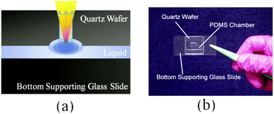 | ||
| Fig. 1 (a) Quartz through-pore fabrication by “sandwiched” drilling method. (b) Fabrication setup, with UV-absorbing liquid confined in a PDMS chamber below the quartz wafer. | ||
Ion channel experiments
Voltage-clamp experiments with ion channels were conducted with a modified Port-a-Patch system (Nanion Technologies GmbH, Munich, Germany). Solutions of 1 M KCl, 10 mM HEPES were used as bath solutions and Ag/AgCl electrodes were used for current recordings. Giant unilamellar vesicles (GUVs), consisting of diphytanoyl phosphocholine lipids (Avanti Polar Lipids, Inc., Alabaster, AL, USA), were formed with a Vesicle Prep Pro (Nanion Technologies GmbH, Munich, Germany).Bilayer formation was monitored resistively and capacitively, and gigaohm seals were ensured. Upon bilayer formation, Alamethicin (Sigma-Aldrich, St. Louis, MO, USA) was injected into the cis compartment and discreet current bursts were subsequently detected, signifying ion channel formation.
Results and discussion
UV-absorbing liquid-based pore fabrication
It has previously been shown that applying a “sandwich” drilling method (i.e., sandwiching a liquid between two substrates during excimer laser ablation) will successfully fabricate micro- and nano-scale through-pores in borosilicate glass.38,39 Theses pores are extremely smooth and are surrounded by a crater-like structure. To apply this technique to piezoelectric quartz, we focus the laser beam on the backside of the quartz wafer, where it interfaces with a liquid media.34,40 Our setup is illustrated in Fig. 1. Different solutions, including de-ionized (DI) water and acetone, are placed in contact with the quartz substrate. These solutions are used because of their large difference in coefficient of volumetric thermal expansion (210 × 10−6 K−1 and 1430 × 10−6 K−1, respectively).41 Moreover, these solutions absorb UV light quite differently. At a wavelength of 193 nm, their UV absorption coefficients are 0.1 cm−1 and 15.4 cm−1, respectively.42,43Fig. 2 shows scanning electron microscope (SEM) images of the quartz surfaces following sandwiched laser ablation. The laser output power is fixed at 5 W and the variable attenuator is set to 73% of total beam transmission. The laser is pulsed 2500 times at 100 Hz. When using DI water (Fig. 2a), significant cracks form on the bottom surface of the quartz substrate. These cracks are concentric rings, appearing deeper and closer to one another as one moves toward the central pore. During pore formation, nanosecond laser irradiation at the quartz/liquid interface ionizes some of the mass in the vapor plume due to the inverse Bremsstrahlung process, forming a microplasma in the vicinity of the quartz substrate.44 According to shadowgraph studies, subsequent expansion of the plasma generates a shock wave.45 Without a sufficient thermal, stabilizing force, these shock waves form uneven surfaces surrounding the pore. In contrast, no cracks are observed for sandwiched laser ablation with acetone, as shown in Fig. 2b. In this case, the surface of the pore is extremely smooth, due to acetone's large thermal expansion and UV absorption coefficients.
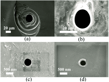 | ||
| Fig. 2 (a) Through-pore fabricated using DI water as the UV-absorbing liquid. (b) Result when using acetone instead of water. (c) Sub-micron pore, fabricated with acetone. (d) Sub-micron pore, fabricated with acetone, highlighting the smoothness of the pore. | ||
Though effective in fabricating smooth, submicron pores in single crystal quartz, acetone evaporates quickly under ambient temperature and is, therefore, difficult to control. As an alternative, we use immersion oil (Cargille Laboratories, Type DF). The thermal expansion and UV absorption coefficients for this oil are 700 × 10−6 K−1 and 1.46–1.65 cm−1, respectively, which are between those of DI water and acetone. Using this oil, we have fabricated pores with a wide range of sizes, from sub-micrometre pores (216 nm diameter minimum) to 30 μm diameter pores. A sample pore formed with this technique is shown in Fig. 3a. The pore size has been fine-tuned by adjusting the laser pulse repetition frequency, the number of corresponding pulses, and the beam transmission rate. In accordance with successful techniques used with borosilicate glass,38 we have used a sequence of two repetition frequencies, first at 50 Hz and then at 100 Hz, and adjusted the number of corresponding pulses for each. Table 1 shows these results, where the effect of transmission rate on pore size is clearly evident. In these cases, the laser power is fixed at 5 W. We find that pore diameters are very sensitive to transmission rates. As shown in Table 1, a 4% decrease from an 87% transmission rate can result in a ten-fold decrease in pore diameter. Such decreases can result in sub-micrometre pores, even approaching the wavelength (193 nm) of the laser used. Also, in both transmission cases, there is a threshold in terms of the number of pulses (>2000) irradiated on quartz at the low repetition frequency (50 Hz), beyond which the pore size rapidly increases.
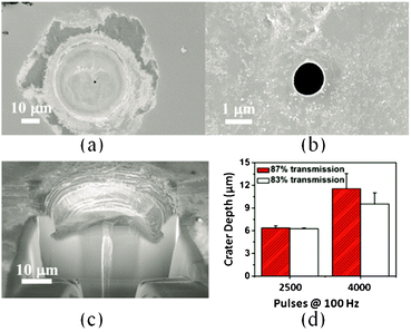 | ||
| Fig. 3 (a) Quartz crater with a small pore in the centre. (b) Zoomed-in view of the pore. (c) FIB milling reveals radial crater features. (d) Relationship between the crater depth, transmission rate, and the number of 100 Hz laser pulses. | ||
In addition to forming a through-pore, we find that using oil as an absorbing media results in a unique crater feature around the pore, as shown in Fig. 3a,c. Different drilling recipes, mentioned above, have little effect on the crater diameter, which is consistently around 40 μm. Fig. 3c is a cross-sectional view of the pore-crater structure after milling with a focused ion beam (FIB). The crater has a relatively flat bottom surface, with an undercut that extends radially into the sidewall. The depth of the crater can be adjusted by tuning the laser parameters, as shown in Fig. 3d. We find that the crater depth is highly sensitive to the number of 100 Hz pulses applied to it. This is more obvious at higher transmission rates, where the crater depth more than doubles, from 6 μm to 13.5 μm, as the number of 100 Hz pulses increases from 2500 to 4000.
Piezoelectric tuning of quartz pores
A unique advantage to fabricating through-pores in single crystal quartz is that they are piezoelectric. An electric field applied across the thickness of the substrate induces an inherent mechanical tension, deforming the substrate and, in the process, tuning the size and shape of the pore. The quartz substrate used in this study is AT-cut quartz, which is a common cut of quartz, owing to its high temperature-frequency stability and its lack of stray coupling between vibrational modes.46 An electric field applied across the thickness of the substrate excites its thickness shear mode. For uni-modal excitation, this results in a translocation of the top face of the pore. However, by exciting opposing thickness shear modes, the central pore deforms. This is accomplished by applying two electric fields of opposite polarity across the thickness of the substrate on either side of the pore, as shown in Fig. 4a. Depending on the polarities of these fields, it is possible to contract or expand the pore. Fig. 4b shows contraction of the pore by applying +1.2 MV m−1, where the measured diameters (per hash-mark lengths) are 33.0 μm and 35.2 μm in the x- and y-direction, respectively. Fig. 4c shows the pore in the absence of applied voltage, with a diameter of 33.4 μm in the x-direction and 35.6 μm in the y-direction. Fig. 4d shows expansion of the same pore by applying −4.3 MV m−1, where the measured diameters (per hash-mark lengths) become 33.9 μm and 38.6 μm in the x- and y-direction, respectively. Previous studies over multiple voltages yield an average deformation of 0.11 μm (MV m−1)−1 in the x-direction and 0.36 μm (MV m−1)−1 in the y-direction.15 For the pore shown in Fig. 4, this results in deformations on the order of 100 nm (MV m−1)−1. By applying electric fields on the order of kV m−1, therefore, subnanometre deformations are possible.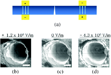 | ||
| Fig. 4 (a) Setup for piezoelectric deformation of AT-cut quartz through-pores. (b) Contracting the pore with +1.2 MV m−1. (c) The pore with no applied bias. (d) Expanding the pore with −4.3 MV m−1. Scale bars are 10 μm. | ||
We also demonstrate ion channel recordings over these pores.15,28 We have formed a planar lipid bilayer over the piezoelectric pore via bursting GUVs. Adhesion between the bilayer and the piezoelectric substrate has been achieved via hydrophilic interactions, which is ensured by cleaning of the quartz substrate with a heated piranha solution (3![[thin space (1/6-em)]](https://www.rsc.org/images/entities/char_2009.gif) :1 ratio of H2SO4:(30%)H2O2) prior to experimentation. Alamethicin ion channels were then inserted into the bilayer and current bursts at multiple different levels of piezoelectric tension have been recorded. As shown in Fig. 5, piezoelectrically-induced tension in the bilayer enhances the time-averaged conductance states of the Alamethicin ion channels, which has previously been demonstrated.15,47,48 These enhanced conductance states are due to piezoelectric tension in the lipid bilayer, and not density increases in the solution, as the millimetre-sized solution-containing o-rings are open to ambient, minimizing the effect of piezoelectrically-induced density increases. Similarly, the enhanced conductance states are not due to stray electrostatic fields, as control measurements of piezoelectrically actuating a lipid bilayer in the absence of alamethicin monomers showed a change in leakage current of only 280 fA.15 We therefore demonstrate an extremely novel application of these piezoelectric pores by precisely controlling the conductance states of alamethicin ion channels.
:1 ratio of H2SO4:(30%)H2O2) prior to experimentation. Alamethicin ion channels were then inserted into the bilayer and current bursts at multiple different levels of piezoelectric tension have been recorded. As shown in Fig. 5, piezoelectrically-induced tension in the bilayer enhances the time-averaged conductance states of the Alamethicin ion channels, which has previously been demonstrated.15,47,48 These enhanced conductance states are due to piezoelectric tension in the lipid bilayer, and not density increases in the solution, as the millimetre-sized solution-containing o-rings are open to ambient, minimizing the effect of piezoelectrically-induced density increases. Similarly, the enhanced conductance states are not due to stray electrostatic fields, as control measurements of piezoelectrically actuating a lipid bilayer in the absence of alamethicin monomers showed a change in leakage current of only 280 fA.15 We therefore demonstrate an extremely novel application of these piezoelectric pores by precisely controlling the conductance states of alamethicin ion channels.
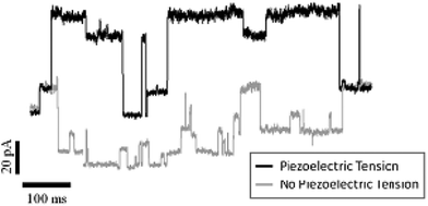 | ||
| Fig. 5 Current traces from Alamethicin ion channels embedded in a planar lipid bilayer suspended over a piezoelectric quartz through-pore. Traces are shown with (black) and without (grey) piezoelectric deformation of the pore. | ||
Conclusions
In conclusion, we demonstrate a one-step micromachining process for fabricating micro- and nanopores in single crystal quartz. Though single crystal quartz is transparent to UV irradiation, we show that ArF excimer laser excitation of a backside, UV-absorbing liquid is capable of forming through-pores. Our research suggests that liquids with large thermal expansion and UV absorption coefficients more effectively form smooth pore surfaces. By using fluorescence immersion oil, pores with diameters comparable to the laser wavelength have been achieved. This technique simultaneously forms craters with relatively flat bottom surfaces centred around the through-pores. These craters could be used for trapping or stabilizing cells in biological experiments. Moreover, we dynamically tune the pore size and shape by applying biasing signals across the thickness of the quartz substrate. This provides an avenue for the exploration of mechanosensitive, biological effects.Acknowledgements
The authors acknowledge support by the NSF MRSEC-IRG1 (National Science Foundation Materials Research, Science, and Education Center, Interdisciplinary Research Group 1 - Grant No. DMR-0520527).References
- J. J. Kasianowicz, E. Brandin, D. Branton and D. W. Deamer, Proc. Natl. Acad. Sci. U. S. A., 1996, 93, 13770–13773 CrossRef CAS.
- C. Dekker, Nat. Nanotechnol., 2007, 2, 209–215 CrossRef CAS.
- J. J. Kasianowicz, J. W. F. Robertson, E. R. Chan, J. E. Reiner and V. M. Stanford, Annu. Rev. Anal. Chem., 2008, 1, 737–766 CrossRef CAS.
- H. F. Lecoanet, J.-Y. Bottero and M. R. Wiesner, Environ. Sci. Technol., 2004, 38, 5164–5169 CrossRef CAS.
- J. Li, D. Stein, C. McMullan, D. Branton, M. J. Aziz and J. Golovchenko, Nature, 2001, 412, 166–169 CrossRef CAS.
- N. Fertig, R. H. Blick and J. Behrends, Biophys. J., 2002, 82, 3056–3062 CrossRef CAS.
- M. J. Kim, M. Wanunu, D. C. Bell and A. Meller, Adv. Mater., 2006, 18, 3149–3153 CrossRef CAS.
- J. W. F. Robertson, C. G. Rodrigues, V. M. Stanford, K. A. Rubinson, O. V. Krasilnikov and J. J. Kasianowicz, Proc. Natl. Acad. Sci. U. S. A., 2007, 104, 8207–8211 CrossRef CAS.
- J. E. Reiner, J. J. Kasianowicz, B. J. Nablo and J. W. F. Robertson, Proc. Natl. Acad. Sci. U. S. A., 2010, 107, 12080–12085 CrossRef CAS.
- G. Oukhaled, J. Mathé, A.-L. Biance, L. Bacri, J.-M. Betton, D. Lairez, J. Pelta and L. Auvray, Phys. Rev. Lett., 2007, 98, 158101 CrossRef CAS.
- J. L. Hedrick, R. D. Miller, C. J. Hawker, K. R. Carter, W. Volksen, D. Y. Yoon and M. Trollsås, Adv. Mater., 1998, 10, 1049–1053 CrossRef CAS.
- P. Chen, T. Mitsui, D. B. Farmer, J. Golovchenko, R. G. Gordon and D. Branton, Nano Lett., 2004, 4, 1333–1337 CrossRef CAS.
- M. Wanunu and A. Meller, Nano Lett., 2007, 7, 1580–1585 CrossRef CAS.
- E. C. Yusko, J. M. Johnson, S. Majd, P. Prangkio, R. C. Rollings, J. Li, J. Yang and M. Mayer, Nat. Nanotechnol., 2011, 6, 253–260 CrossRef CAS.
- E. Stava, M. Yu, H. C. Shin, H. Shin, J. Rodriguez and R. H. Blick, Lab Chip, 2012, 12, 80–87 RSC.
- G. R. Willmott, R. Vogel, S. S. C. Yu, L. G. Groenewegen, G. S. Roberts, D. Kozak, W. Anderson and M. Trau, J. Phys.: Condens. Matter, 2010, 22, 454116 CrossRef CAS.
- K. G. Klemic, J. F. Klemic, M. A. Reed and F. J. Sigworth, Biosens. Bioelectron., 2002, 17, 597–604 CrossRef CAS.
- N. Fertig, M. Klau, M. George, R. H. Blick and J. C. Behrends, Appl. Phys. Lett., 2002, 81, 4865–4867 CrossRef CAS.
- J. M. Nagarah, E. Paek, Y. Luo, P. Wang, G. S. Hwang and J. R. Heath, Adv. Mater., 2010, 22, 4622–4627 CrossRef CAS.
- D. Tabor, Rev. Phys. Technol., 1970, 1, 145–179 CrossRef.
- M. A. T. M. Broekmans, Mater. Charact., 2004, 53, 129–140 CrossRef CAS.
- W. A. Deer, R. A. Howie and J. Zussman, The Rock-Forming Minerals, Longmans, Green and Co. Ltd., London, 1963 Search PubMed.
- K. Benndorf, Single-Channel Recording, ed. B. Sakmann and E. Neher, Plenum Press, New York, 1995 Search PubMed.
- V. Tabard-Cossa, D. Trivedi, M. Wiggin, N. N. Jetha and A. Marziali, Nanotechnology, 2007, 18, 305505 CrossRef.
- R. M. M. Smeets, U. F. Keyser, M. Y. Wu, N. H. Dekker and C. Dekker, Phys. Rev. Lett., 2006, 97, 088101 CrossRef CAS.
- R. M. M. Smeets, U. F. Keyser, N. H. Dekker and C. Dekker, Proc. Natl. Acad. Sci. U. S. A., 2008, 105, 417–421 CrossRef CAS.
- E. Neher and B. Sakmann, Nature, 1976, 260, 799–802 CrossRef CAS.
- E. Stava, M. Yu, H. Shin and R. H. Blick, IEEE Trans. NanoBiosci., 2010, 9, 307–309 CrossRef.
- R. A. Levis and J. L. Rae, Biophys. J., 1993, 65, 1666–1677 CrossRef CAS.
- W. Blaker and P. Schaeffer, Optics: An Introduction for Technicians and Technologists, Prentice-Hall, New Jersey, 2000 Search PubMed.
- J. Koch, F. Korte, C. Fallnich, A. Ostendorf and B. N. Chichkov, Opt. Eng., 2005, 44, 051103 CrossRef.
- D. F. Farson, H. W. Choi, B. Zimmerman, J. K. Steach, J. J. Chalmers, S. V. Olesik and L. J. Lee, J. Micromech. Microeng., 2008, 18, 035020 CrossRef.
- R. B. Laughlin, Phys. Rev. B, 1980, 22, 3021–3029 CrossRef CAS.
- J. Wang, H. Niino and A. Yabe, Appl. Phys. A: Mater. Sci. Process., 1999, 68, 111–113 CrossRef CAS.
- G. Kopitkovas, T. Lippert, C. David, A. Wokaun and J. Gobrecht, Thin Solid Films, 2004, 453–454, 31–35 CrossRef CAS.
- G. Kopitkovas, V. Deckert, T. Lippert, F. Raimondi, C. W. Schneider and A. Wokaun, Phys. Chem. Chem. Phys., 2008, 10, 3195–3202 RSC.
- V. Liberman, M. Rothschild, P. G. Murphy and S. T. Palmacci, J. Vac. Sci. Technol., B, 2002, 20, 2567–2573 CAS.
- M. Yu, H. S. Kim and R. H. Blick, Opt. Express, 2009, 17, 10044–10049 CrossRef CAS.
- R. H. Blick, M. Yu, H. Qin and H.-S. Kim, U.S. Patent 8,092,739, Jan. 2012 Search PubMed.
- R. H. Blick and M. Yu, U.S. Patent 2011/0111179, May 2011 Search PubMed.
- Y. S. Touloukian, R. K. Kirby, E. R. Taylor and T. Y. R. Lee, Thermophysical Properties of Matter, Plenum Press, New York, 1971 Search PubMed.
- P. T. Staveteig and J. T. Walsh, Appl. Opt., 1996, 35, 3392–3403 CrossRef CAS.
- Y. Badr, S. A. El-wanees and M. A. Mahmoud, J. Photochem. Photobiol., A, 2004, 168, 31–38 CrossRef CAS.
- R. E. Russo, X. L. Mao, J. H. Yoo and J. J. Gonzalez, Laser-Induced Breakdown Spectroscopy, ed. J. P. Singh and S. N. Thakur, Elsevier, Amsterdam, 2007 Search PubMed.
- X. Z. Zeng, X. L. Mao, S. B. Wen, R. Greif and R. E. Russo, J. Phys. D: Appl. Phys., 2004, 37, 1132–1136 CrossRef CAS.
- Piezoelectricity, ed. W. J. Cady, Dover Publications, New York, 1964 Search PubMed.
- L. R. Opsahl and W. W. Webb, Biophys. J., 1994, 66, 71–74 CrossRef CAS.
- S. L. Keller, S. M. Bezrukov, S. M. Gruner, M. W. Tate, I. Vodyanoy and V. A. Parsegian, Biophys. J., 1993, 65, 23–27 CrossRef CAS.
Footnote |
| † These authors contributed equally. |
| This journal is © The Royal Society of Chemistry 2013 |