Magnetic field induced capacitance enhancement in graphene and magnetic graphene nanocomposites†
Jiahua Zhua, Minjiao Chena, Honglin Quab, Zhiping Luoc, Shijie Wud, Henry A. Coloradoe, Suying Wei*b and Zhanhu Guo*a
aIntegrated Composites Laboratory (ICL), Dan F Smith Department of Chemical Engineering, Lamar University, Beaumont, TX 77710, USA. E-mail: zhanhu.guo@lamar.edu; Tel: +1 (409) 880-7654
bDepartment of Chemistry and Biochemistry, Lamar University, Beaumont, TX 77710, USA. E-mail: suying.wei@lamar.edu; Tel: +1 (409) 880-7976
cDepartment of Chemistry and Physics, Fayetteville State University, Fayetteville, NC 28301, USA
dAgilent Technologies, Inc, Chandler, AZ 85226, USA
eDepartment of Mechanical and Aerospace Engineering, University of California Los Angeles, Los Angeles, CA 90095, USA
First published on 22nd October 2012
Abstract
Magnetic graphene nanocomposites (MGNCs) synthesized by a facile thermal decomposition method have been introduced. TEM observations reveal a uniform distribution of the Fe2O3 nanoparticle size and preferential nuclei growth along the edge defects. Both graphene and its Fe2O3 nanocomposites are prepared as electrochemical electrodes to evaluate their capacitor performances. Under normal conditions (without a magnetic field), the MGNCs show lower capacitance than graphene due to the large particle loading (52.5 wt%), which brings larger internal resistance and thus prevents efficient electron transportation within the electrodes. However, in the presence of an external magnetic field, both graphene and MGNC electrodes exhibit significantly enhanced capacitance as compared to the results obtained under normal conditions. Specifically, the capacitance of graphene is increased by 67.1 and 26.8% at the sweeping rates of 2 and 10 mV s−1, respectively. Even larger enhancements of 154.6 and 98.2% were observed in MGNCs at the same sweeping rates of 2 and 10 mV s−1, respectively. The energy density and power density of the electroactive materials are also dramatically enhanced in the presence of a magnetic field. Equivalent circuit modeling of impedance spectra revealed that the magnetic field played a critical role in restricting the interfacial relaxation process and thus enhanced the electrode capacitance. These findings present a potential revolution of traditional electrochemical capacitors by simply applying an external magnetic field to enhance the capacitance dramatically (even doubling it depending on the electroactive materials) without material replacement and structural modification.
Broader contextTremendous efforts have been made to improve the energy density and power density of electrode materials for supercapacitor applications. However, until now, all the efforts have been made focusing on the inside of the capacitor including new electrodes, electrolyte materials, and capacitor configuration designs. In this work, a significant small external magnetic field (720 Gauss) induced capacitance enhancement is reported for graphene and graphene nanocomposite electrodes. At voltage scan rates of 2 and 10 mV s−1, the capacitance of graphene increased by 67.1 and 26.8%. Even larger enhancements of 154.6 and 98.2% were observed in the magnetic graphene nanocomposites at the same sweeping rates. The external magnetic field was believed to improve the energy state of electrons and thus prompt the electron transportation at the electrolyte/electrode interface (double layer) during testing. Without any modification of the inside of the electrochemical capacitance cell, the reported magnetic field enhanced capacitance with both improved energy density and power density will have a great impact on the electrochemical energy storage field. |
1. Introduction
The two dimensional (2D) single carbon atomic thick graphene arranged as a honeycomb lattice has unique electron and phonon transport1–5 and possesses wide potential applications such as in nanoscale devices.6–11 Both theoretical and experimental research efforts have indicated that the electronic energy dispersion in graphene is different from in conventional 2D materials. Specifically, the electron and hole bands are linear near K and K′ points of the Brillouin zone in 2D graphene. However, the electron energy depends quadratically on the electron momentum in a conventional 2D system.12 Various unusual transport phenomena are related to the fact that graphene behaves as a 2D electronic system, and the conduction and valence bands meet at the Dirac point, where the Fermi energy position is located.13In recent years, metal oxide nanostructures have been decorated on graphene sheets to incorporate multifunctionalities into one hybrid material. For example, TiO2 nanoparticles (NPs) have been grown on graphene to enhance the photocatalytic activity in the degradation of rhodamine B14 and for enhanced Li-ion insertion properties,15 Pt-on-Pd bimetallic nanodendrites supported on graphene sheets could serve as advanced catalysts for methanol oxidation,16 a magnetite–graphene composite has demonstrated a high adsorption capacity for As(III) and As(V) from polluted water,17,18 and an Fe@Fe2O3/Si–O–S core@double-shell structure coated on graphene exhibits much faster and complete adsorption of Cr(VI) within a wide range of pH conditions.19 Among these applications, electrochemical capacitance has become one of the most active research areas due to the urgent need for advanced energy storage technology in hybrid vehicles that require high energy density and power density output.
Graphene is often obtained from the reduction of graphite oxide by various reduction approaches20 and has been demonstrated as a promising candidate for supercapacitor application.21–23 To enhance the capacitance, many approaches have been developed especially coating electroactive organic and inorganic nanostructures on the graphene sheets with the aim to enhance the effective surface area and introduce additional pseudocapacitance. For example, flexible polyaniline (PANI) film–graphene composite paper was produced via an in situ anodic electropolymerization process and this material generated a capacitance of 233 F g−1.24 To reach a higher energy storage density, PANI nanowire arrays25 and PANI nanofibers (PANI-NFs)26 have been successfully grafted on graphite oxide (GO) sheets using a rapid mixing reaction method and the composite materials reach capacities as high as 555 and 480 F g−1, respectively. The inorganic materials which obtain the highest theoretical capacitance values are MnO2 (600–700 F g−1)27 and RuO2 (720–900 F g−1).28 As a hybrid structure with graphene, MnO2 nanowire–graphene has been developed as electrodes for electrochemical capacitors, which exhibit a capacitance as high as 216 F g−1.29 Other composites such as RuO2–graphene and Fe3O4–graphene are observed to obtain high capacitances of 265 and 180 F g−1, respectively.30
Even though the fast development of capacitor electrodes has enhanced the capacitance dramatically, it is still a great challenge to further improve the capacitance from the composition and structural modifications of currently available materials. The charge/discharge process of a capacitor would be regarded as controlled charge carrier movement in the system. In the presence of an external magnetic field, the electron polarization and transportation would be significantly different compared to under normal conditions (without field). Even though the electrical field induced magnetic field in the capacitor has been studied in previous literature,31 how the external magnetic field affects the electrochemical performance of the capacitor has been rarely reported until now. Especially in graphene, the external magnetic field could affect its resistance, often called magnetoresistance.32–37 Therefore, the magnetic field would definitely affect the capacitance performance of graphene. With regard to magnetic graphene nanocomposites (MGNCs), the magnetic field effect on the electrochemical performance would be even more complex due to the existence of magnetic NPs. To the best of our knowledge, the importance of the external magnetic field effect on the capacitance performance has not been realized yet. However, it is essentially important to explore the magnetic field effect on the capacitor performance of graphene and its MGNCs.
Here we report a facile one-step synthesis approach to prepare Fe2O3–graphene hybrid nanostructures. An organic iron precursor, iron pentacarbonyl, which is immiscible with a graphene–dimethylformamide suspension, was used to in situ synthesize magnetic nanoparticles on graphene sheets with uniform distribution. This method would be applied to synthesize other high quality metal oxide–graphene nanocomposites without using any surfactants. The microstructures of graphene and its MGNCs were carefully characterized by electron microscopies (TEM, AFM and SEM). The electrochemical performance of the graphene and MGNCs was studied by cyclic voltammetry (CV), galvanostatic charge/discharge and electrochemical impedance spectroscopy tests. The influence of an external magnetic field supplied by an electromagnet on the electrochemical performance of the same electrodes was evaluated as well.
2. Experimental
2.1 Materials
Natural graphite powder (SP-1) was purchased from Bay Carbon Inc, USA. Iron(0) pentacarbonyl (Fe(CO)5, 99.99%), sulfuric acid (H2SO4, 95.0–98.0%), hydrochloric acid (HCl, 36.5–38.0%), potassium persulfate (K2S2O8, ≥99.0%), phosphorus pentoxide (P2O5, ≥98.0%), potassium permanganate (KMnO4, ≥99.0%), H2O2 solution (PERDROGEN® 30% H2O2 (w/w)), hydrazine monohydrate, and polyvinylidene difluoride (PVDF) membrane filter (Durapore® PVDF) were all purchased from Sigma Aldrich. The dialysis membrane (Spectra/Por 4, molecular weight cut off (MWCO): 12![[thin space (1/6-em)]](https://www.rsc.org/images/entities/char_2009.gif) 000–14000) was purchased from Spectrum Laboratories, Inc. Nickel foam was purchased from Goodfellow corporation with a thickness of 1.6 mm and porosity of 95%. Chloroform (CHCl3), ammonia (28%, lab grade), and dimethylformamide (DMF) were purchased from Fisher Scientific. All the materials were used as received without any further treatment.
000–14000) was purchased from Spectrum Laboratories, Inc. Nickel foam was purchased from Goodfellow corporation with a thickness of 1.6 mm and porosity of 95%. Chloroform (CHCl3), ammonia (28%, lab grade), and dimethylformamide (DMF) were purchased from Fisher Scientific. All the materials were used as received without any further treatment.2.2 Synthesis of graphite oxide (GO) and reduced-GO (graphene)
The graphite oxide (GO) was synthesized from natural graphite powder following the modified Hummers method.38,39 Specifically, an additional graphite oxidation was applied prior to the GO preparation according to the Hummers method. The pre-oxidation step was essentially important to produce complete oxidation products. Briefly, the graphite powder (3.0 g) was put into an 80 °C solution containing concentrated H2SO4 (12.0 mL), K2S2O8 (4.0 g), and P2O5 (4.0 g). The resultant dark blue mixture was thermally isolated and allowed to cool down to room temperature over a period of 6 hours. The mixture was then carefully diluted with distilled water, filtered, and washed on the PVDF membrane until the rinsing water became neutral. The product was dried in air at ambient temperature overnight. This preoxidized graphite was then subjected to oxidation by the Hummers method. The oxidized graphite powder was put into 0 °C concentrated H2SO4 (120.0 mL). KMnO4 (15.0 g) was added gradually with stirring and cooling. The temperature of the mixture was not allowed to reach 20 °C. The mixture was then stirred at 35 °C for 2 hours, and distilled water (250.0 mL) was added. In 15 min, the reaction was terminated by adding a large amount of distilled water (700 mL) and H2O2 solution (20.0 mL), after which the mixture turned to bright yellow. The mixture was filtered and washed with 1:10 HCl solution (1.0 L) to remove metal ions. The GO product was suspended in distilled water to give a viscous brown 2.0 wt% dispersion, which was subjected to dialysis to completely remove metal ions and acids. The final concentration of GO solution was 1.4 wt% determined by thermogravimetric analysis.The graphene was chemically reduced from GO solution. Typically, 40.0 g 1.4 wt% GO solution was magnetically stirred and simultaneously 100 mL ammonium hydroxide was added to the GO solution. After further reduction by adding 7.5 mL hydrazine monohydrate, the mixture was heated to 90 °C and maintained there for one hour. Then the reduced GO (graphene) was filtrated and vacuum dried at 60 °C.
2.3 Synthesis of Fe2O3–graphene nanocomposites (MGNCs)
The MGNCs were fabricated using a one-pot thermodecomposition method. To be specific, graphene (0.140 g) was dispersed in DMF (100.0 mL) using ultrasonication for two hours at room temperature. Then, Fe(CO)5 (0.385 g) was injected into the graphene–DMF solution (DMF and Fe(CO)5 are intermiscible) and sonicated for another half hour. The suspension was heated to the boiling temperature (∼153 °C) and refluxed for additional four hours. After that, the Fe2O3–graphene nanocomposites were formed in the DMF solution. Both graphene–DMF and MGNCs–DMF solutions were maintained in sealed vials for further electrode preparation.2.4 Characterization
The morphology of graphene and its MGNCs was characterized by field emission scanning electron microscopy (SEM, JEOL JSM-6700F). The particle size and crystalline structure in the MGNCs were further characterized by field emission transmission electron microscopy (TEM, FEI Tecnai G2 F20), operated at an accelerating voltage of 200 kV. The TEM samples were prepared by drying a drop of sample–ethanol suspension on carbon-coated copper TEM grids.The three dimensional structures of graphene and its MGNCs were characterized by atomic force microscopy (AFM, Agilent 5600 AFM system with multipurpose 90 mm scanner). Imaging was done in acoustic ac mode (AAC) using a silicon tip with a force constant of 2.8 N m−1 and a resonance frequency of 70 kHz. The sample was prepared by sonicating the powders in water for 15 min to form an aqueous suspension, drop-casting some suspension on a freshly cleaved mica slide, and then drying in air overnight. The sample surface was blown with compressed nitrogen to remove any possible loose particles on the surface before imaging.
The powder X-ray diffraction analysis of the samples was carried out with a Bruker AXS D8 Discover diffractometer with GADDS (General Area Detector Diffraction System) operating with a Cu-Kα radiation source filtered with a graphite monochromator (λ = 1.5406 Å). The detector used was a HISTAR two-dimensional multi-wire area detector. The samples were loaded onto double sided scotch tape, placed on a glass slide, and mounted on a quarter-circle Eulerian cradle (Huber) on an XYZ stage. The X-ray beam was generated at 40 kV and 40 mA power and was collimated to about an 800 μm spot size on the sample. The incident ω angle was 5°. A laser/video system was used to ensure the alignment of the sample position on the instrument center. XRD scans were recorded from 5 to 70° for 2θ with a 0.050° step-width and a 60 s counting time for each step.
The thermal degradation of graphene and its MGNCs was studied by thermo-gravimetric analysis (TGA, Q-500, TA instruments) from 25 to 700 °C with an air flow rate of 60 mL min−1 and a heating rate of 10 °C min−1.
The compositions of all the samples were analyzed by X-ray photoelectron spectroscopy (XPS). XPS measurements were conducted on a Kratos AXIS 165 system. Analysis of each sample started with a quick survey scan in the binding energy range from 1200 to 0 eV at the pass energy level of 40 eV to check all the possible elements existing in the sample, followed by the high-resolution scan of each element at the pass energy level of 160 eV to obtain the compositional results. Both survey scan and high resolution scans were carried out with a Mono Al X-ray source at the anode of 10 kV and beam current of 15 mA.
2.5 Preparation of supercapacitor electrodes and electrochemical evaluation
Supercapacitor electrodes were prepared via a simple dipping method without using any binders or conductive additives. Specifically, nickel foam (1.0 × 4.0 cm) was partially immersed (immersion depth: ∼1.0 cm) in the as-prepared graphene–DMF solution for 10 seconds. After that, the nickel foam was heated in a vacuum oven at 100 °C for 12 hours and graphene would tightly adhere to the nickel foam after drying. The microstructures of nickel foam and electrodes after loading electroactive materials are shown in Fig. S1.† Nickel foam was weighed before and after material loading to obtain the exact weight of the electroactive samples in each electrode. The MGNC electrode was prepared following the same procedures.Supercapacitor characterization was carried out in a three-electrode cell using platinum wire and Ag/AgCl as the counter and reference electrode, respectively. 1.0 M Na2SO4 was used as an electrolyte. All electrochemical measurements were conducted using a VersaSTAT 4 potentiostat (Princeton Applied Research). CV measurements were performed at different voltage scan rates in a range from 2 to 50 mV s−1. Galvanostatic charge/discharge measurements were carried out at different current densities from 0.2 to 10.0 A g−1. To test the electrochemical property of the materials in a magnetic field, the whole electrochemical cell was fixed between two magnetic poles of an electromagnet (EM4-HVA H-Yoke, Lake Shore Cryotronics, Inc. USA), Scheme 1. The magnetic field flux density was controlled through tuning the magnitude of the current, which was measured to be 720.0 G by a Guass/tesla meter (7010 Gauss/tesla meter, Sypris).
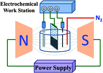 | ||
| Scheme 1 The schematic setup of the electrochemical cell tested in a magnetic field. | ||
3. Results and discussion
The morphologies of graphene and its MGNCs were characterized by SEM and TEM. The pure graphene shows a smooth surface with a folded nature and the particles attaching to the graphene could be observed in MGNCs, Fig. S2.† For further characterizing the MGNCs, the particle size distribution and specific components of the NPs must be identified for a better understanding of the unique electrochemical properties. To address these concerns, both high-resolution TEM (HRTEM) and selected area electron diffraction (SAED) techniques were introduced. The magnetic NPs grown on the graphene sheet were observed to exhibit a narrow size distribution within the range of 12–30 nm, Fig. 1(a). Moreover, the NPs are noticed to preferentially grow along the edge of graphene, the red dashed line in Fig. 1(b). In the graphene plane, no particles could be observed, as marked by the blue dashed circle in Fig. 1(b). This observation provides direct evidence for the NPs growth at defect sites, which is on the edges of graphene. On the defect sites along the edge, dangling bonds or functional groups can react with nanoparticle precursors to afford active oxide growth.40 However, the growth of NPs is difficult on the graphene plane due to the lack of dangling bonds or functional groups, as in the case of carbon nanotubes.41,42 Similar phenomena were also observed in other literature. For example, Al2O3 preferentially grew on the edges of graphene sheets using an atomic layer deposition technique.40 By a solvent-free microwave heating process, Ag NPs preferentially grew at the defect sites of multi-walled carbon nanotubes (MWCNTs).43 Different mechanisms have been proposed to explain the interfacial interaction between NPs and graphene/graphite oxide, which include physisorption, electrostatic binding, and charge transfer interactions.44 It is well known that both the particle dispersion and the particle–particle interaction are strongly related to the amount of NPs and the specific surface area of the graphene sheet. In this work, the edge defects of graphene served as templates to localize the nuclei and these nuclei further grew into NPs at specific locations. Therefore, nearly mono-dispersed NPs were observed on the graphene sheets. The typical average particle size is 19.1 nm, inset of Fig. 1(a). To identify the crystalline structure and specific component of the NPs, an enlarged HRTEM image was taken from a single nanoparticle, Fig. 1(c). A lattice fringe of 2.5 Å corresponds to the (311) plane of Fe2O3. The XRD results are in good agreement with the HRTEM observations (refer to Fig. S3†). The diffraction rings marked with numbers from 1 to 7, Fig. 1(d), correspond to the (220), (311), (440), (430), (521), (620), and (632) crystalline planes of Fe2O3 NPs (PDF#39-1346). The saturated magnetization (Ms) of the MGNCs is 32.3 emu g−1, Fig. S4.†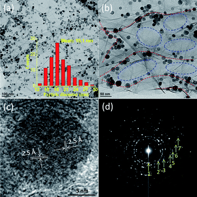 | ||
| Fig. 1 TEM microstructures of the MGNCs. (a) The NPs are uniformly distributed on the graphene sheet (the inset column figure shows the particle size distribution with an average size of 19.1 nm), (b) enlarged magnification of image (a) shows the favorable growth of NPs along the graphene edge indicated by the red dashed line rather than the central area of graphene indicated by the blue dashed circle, (c) a HRTEM image of a single particle showing an interlayer distance of 2.50 Å corresponding to the (311) plane of iron oxide, and (d) a selected area electron diffraction (SAED) pattern of the NPs. The diffraction rings are marked with numbers from 1 to 7 indicating the crystalline phases of iron oxide. | ||
Energy-filtered TEM (EFTEM) was conducted on the sample to further clarify the specific component of the NPs and graphene sheet. The zero loss image (a) and elemental maps of carbon (b), iron (c), and oxygen (d) are shown in Fig. 2. The EFTEM mapping provides a 2-dimensional elemental distribution. A brighter area in the elemental map indicates a higher concentration of the corresponding element in that area. They are shown in different colors, for the purpose of identifying their positions within the MGNCs. Fig. 2(b) depicts the C map, the brighter cracking-shaped area shows the folded nature at the edge or stacking phenomena among individual graphene sheets.19 The Fe map and O map show exactly the same element distribution in Fig. 2(c) and (d), indicating that the NPs have been completely oxidized. Even though the element O could not be obviously observed on the graphene sheet, the reduction is not complete, as evidenced by X-ray photoelectron spectroscopy (XPS) analysis, Fig. S5.† The C–O atomic ratio is 5.95 and 5.86 for graphene and MGNCs, respectively. Summation of Fe and C maps yields Fig. 2(e); the red spherical NPs are observed to be mainly distributed at brighter C areas, which further confirms the proposed growth mechanism. The summation of Fe, C, and O gives the elemental distribution, Fig. 2(f). The yellow spherical spots indicate the complete oxidation of iron and thus the element O is homogeneously distributed within the NPs. This result is different from our previous report of synthesizing core@double-shell NPs while a surfactant was introduced.19
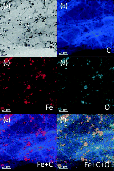 | ||
| Fig. 2 EFTEM of the MGNCs (a) zero-loss image, (b) C map, (c) Fe map, (d) O map, (e) Fe + C map, and (f) Fe + C + O map. | ||
TEM characterization clearly shows the NP size and distribution on a graphene sheet, while it is not able to provide information in three dimensions. Especially, it is hard to identify whether the small amount of the overlapped NPs are from particle stacking on individual graphene sheets or they are overlapped from different sheets. An atomic force microscopy (AFM) height profile can be used to identify the three dimensional structure of the particle–particle interaction, especially the stacking of NPs. Therefore, a dilute suspension of sample was drop-casted onto a mica substrate and analyzed by AFM. Fig. 3(a) and (b) shows the AFM images of pure graphene and MGNCs. Obviously, the cross-section analysis on graphene shows a random distribution of the height profile from 2 to 28 nm, indicating the curved nature of the graphene, Fig. 3(a). In MGNCs, the spherical NPs are deposited directly on the graphene sheet without covalent bonding and the graphene sheet seems to be covered completely by the NPs due to the observation of a sharp edge during the observation of AFM. The particle size is in the range of 12–29 nm with an average size of 19.1 nm as evidenced by the TEM characterization. After decorating NPs in Fig. 3(d), the height profile is mainly located around 20 and 40 nm, indicating the deposited single layer of NPs (marked with single triangle in Fig. 3(d)) and double layer of NPs stacking together (marked with double triangle in Fig. 3(d)), respectively. The slightly higher position of the two peaks at the right end is due to the curving up of graphene sheet.
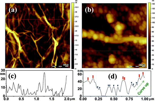 | ||
| Fig. 3 AFM images of (a) graphene and (b) MGNCs; (c) and (d) are the depth profiles of the lines of interest in (a) and (b), respectively. The dashed arrow in (d) depicts the curve up direction of the graphene sheet. The single triangles indicate the single layer of NPs and the double triangles indicate the double layer of NPs stacking together. | ||
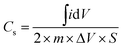
Cyclic voltammetry was studied using the classical three electrode method in 1.0 M Na2SO4 electrolyte to measure the capacitance of graphene and its MGNCs. The graphene with a high specific surface area is expected to be a promising electrode material for electrochemical applications.21Fig. 4(a) shows the CV curves of graphene scanning at a voltage sweeping rate of 2, 5, 10, 20 and 50 mV s−1. The electrodes are stable in the aqueous Na2SO4 solution within the potential range employed (0–0.8 V) and the peaks from faradic current (faradic current always comes with redox reactions where oxidation and reduction peaks would be observed on the CV loop scan) are not observed. The specific capacitance is calculated using the following eqn (1):45
 | (1) |
 is the integrated area of the CV curve, m is the mass of the electrode material in g, ΔV is the scanned potential window in V, and S is the scan rate in V s−1. The Cs of a graphene based supercapacitor is calculated to be 24.7, 24.6, 22.8, 20.2 and 16.1 F g−1 at the voltage sweeping rates of 2, 5, 10, 20 and 50 mV s−1, respectively. The specific capacitance decreases significantly with increasing voltage sweep rate, indicating a lower stability of the capacitance at a higher voltage sweep rate. The graphene electrode in the current work exhibits lower capacitance than other reported values due to the relatively larger resistance as determined by four point probe technique, Fig. S6.† For example, Rakhi et al. reported a capacitance of 150 F g−1 of graphene nanosheets with the voltage sweep rate of 20 mV s−1, using a two symmetric electrode method in 30% KOH electrolyte. Furthermore, the addition of metal oxide (SnO2, MnO2, RuO2) NPs on the graphene substrate further enhanced the capacitance of the electrode materials due to the combined effect of spacers and redox reaction.46 After decorating Fe2O3 NPs on the graphene sheet, the MGNCs based supercapacitors exhibit slightly distorted rectangular CV loops even with a voltage sweep rate up to 50 mV s−1, Fig. 4(b), indicating that the efficient double layer capacitor is well-established in the electrode.47 The smooth rectangular curve without any oxidation or reduction peaks indicates the negligible pseudocapacitance contribution from NPs to the total capacitance of MGNCs. However, a much lower capacitance of MGNCs (<10 F g−1) than that of graphene is observed, which is attributed to the very high loading of non-conductive Fe2O3 NPs in MGNCs (52.5%, refer to ESI, Fig. S7†), which prevents the efficient electron transportation within the electrodes.30 Further evidence from XPS analysis demonstrates that a certain amount of oxygen containing groups still exists on the graphene sheet, which accounts for the larger internal resistance of the electrodes and thus the smaller capacitance. The CV curve of the nickel foam is also measured as a control experiment, Fig. S8,† and the results indicate a negligible capacitance contribution of nickel foam to the total capacitance of the electrode after loading electroactive materials.
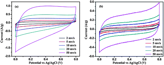 | ||
| Fig. 4 CV loops of the supercapacitor cells based on (a) graphene and (b) MGNCs at different scan rates using 1.0 M Na2SO4 electrolyte. | ||
Fig. 5 shows the galvanostatic charge/discharge curves of graphene and MGNCs tested at current densities of 0.2, 0.5, 1.0, 2.0, 5.0 and 10.0 A g−1. Graphene exhibits a nearly linear and symmetric charge/discharge profile at different current densities, Fig. 5(a). The specific capacitance at different current densities is calculated by eqn (2)48 from the discharge curves,
 | (2) |
 | ||
| Fig. 5 Galvanostatic charge/discharge curves of (a) graphene and (b) MGNCs with specific current densities in 1.0 M Na2SO4 electrolyte. | ||
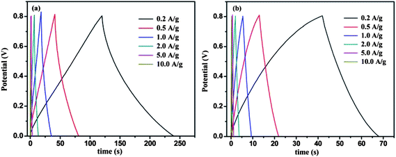
The electrochemical performance of capacitors in a magnetic field has been rarely studied until now. Inspired by the changes of electron spin energy states in an applied magnetic field,49 unique electrochemical performance is expected when the electrode is tested in an external magnetic field. Fig. 6(a) and (b) show the CV loops of graphene at a voltage sweeping rate of 2 and 10 mV s−1, respectively, with and without magnetic field (W/O MF). It is obvious that the CV loops of graphene become significantly broader after applying the MF, while the typical rectangular shape is still maintained, Fig. 6(a) and (b). After applying an external MF around the electrodes, the calculated capacitance increased by 67.1 and 26.8% at sweeping rates of 2 and 10 mV s−1, respectively. This significant capacitance enhancement is attributed to the improved energy state of the electron (±μeH) in a magnetic field H. μe, μe = −gβS, is the magnetic moment associated with its spin state, g is dimensionless constant called the “electron g-factor”, β is the electronic Bohr magneton, and S is the electron spin.49 In the absence of a magnetic field, the energy of an electron with spin quantum number ms = +1/2 is indistinguishable from that for ms = −1/2, often called degeneracy.50 However, in the presence of a magnetic field, the degeneracy is lifted and different energies of the “+” and “−” spin states arise, leading to a difference of energy levels hν = gβH, where hν is the quantum of energy corresponding to a characteristic frequency ν (depending on H).49 Therefore, the enhanced energy state of the electrons would definitely increase the electron transportation efficiency at the electrolyte–electrode interfacial area (double layer area) during electrochemical process and thus improve the capacitance performance. With regard to the MGNCs, the CV loops under an external MF become broader and distorted in shape, Fig. 6(c) and (d), especially at higher potential ranges where the curve deviates from the one obtained without MF. At a low voltage sweeping rate of 2 mV s−1, the two CV loops become isolated and not overlapped between each other, which further confirms the significance of MF on the MGNC electrode. The capacitance is surprisingly enhanced by 154.6 and 98.2% in an external MF at the sweeping rates of 2 and 10 mV s−1, respectively, which is significantly larger than the enhancement observed in graphene electrode. It has been stated above that the large number of magnetic Fe2O3 nanoparticles increases the resistance of the MGNCs, which is detrimental to the capacitance enhancement. However, these nanoparticles could serve as a spacer between graphene layers and provide a larger electrolyte–electrode interfacial area (double layer area) than graphene. Therefore, the MF has an even more significant effect on capacitance enhancement of the MGNCs. In addition, it is worth mentioning that the CV curves of the MGNCs are tilted to higher current density in the presence of MF, indicating a reduced internal resistivity in the MF that contributes to the capacitance enhancement of the electrodes.
 | ||
| Fig. 6 Comparison of CV loops of graphene tested at voltage sweeping rates of (a) 2 and (b) 10 mV s−1, and MGNCs tested at (c) 2 and (d) 10 mV s−1 in 1.0 M Na2SO4 electrolyte. “W/O MF” means the electrodes were tested without a magnetic field, “With MF” indicates the measurement was recorded in a magnetic field. | ||
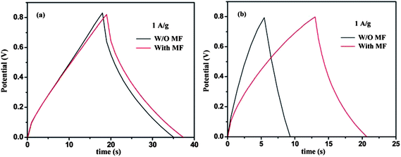
The MF effect on the charge/discharge performance of graphene and its MGNCs was also investigated under the current density of 1 A g−1, Fig. 7. Graphene, Fig. 7(a), gives a similar charge/discharge curve pattern with elongated discharge time under a MF and the corresponding capacitance in a MF calculated by eqn (2) is increased by 5.9% as compared to normal conditions. At the same current density, the MGNCs demonstrate much larger discharge times under the MF, Fig. 7(b), which brings an enhancement of 92.5% in capacitance. These results are highly consistent with the observations from CV measurements, Fig. 6.
 | ||
| Fig. 7 Galvanostatic charge/discharge curves of (a) graphene and (b) MGNCs tested without or with a MF at a constant current density of 1.0 A g−1 in 1.0 M Na2SO4 electrolyte. | ||
Energy density (E) and power density (P) of the capacitors are calculated from eqn (3) and (4), respectively.51
 | (3) |
 | (4) |
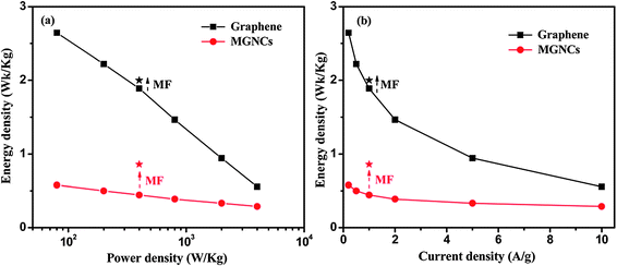
The E as a function of P and current density is shown in Fig. 8(a) and (b) and a gradual decrease of E is observed with increasing P and current density. The E of graphene is in the range of 0.5–3 Wh kg−1, which is consistent with the values reported in most of the carbon based electrochemical capacitors.52,53 The MGNCs show much lower E (∼0.5 Wh kg−1) compared to graphene due to the larger internal resistance after decorating with Fe2O3 NPs. The star symbol represents the energy density of the electrodes in a MF at the same power density and current density as marked by the dashed arrow in Fig. 8(a) and (b). The large enhancement of E in the MF reveals that the electrodes are able to provide almost doubled E when they are placed in an external MF.
 | ||
| Fig. 8 Energy density as a function of (a) power density, and (b) current density of the electrodes in 1.0 M Na2SO4 electrolyte. The data (circular and square symbols with lines) were recorded without a MF, and the stars indicate measurements which were recorded at a current density of 1 A g−1 in the presence of external MF. | ||
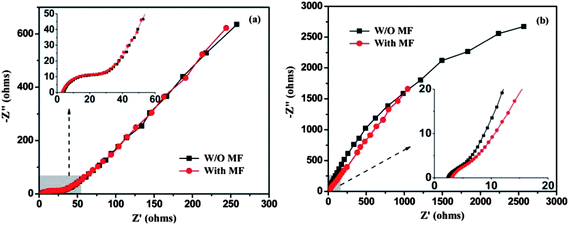
The electrical impedance spectroscopy (EIS) technique has been employed to understand the difference in the electrochemical behaviors of graphene and its MGNCs. EIS was done using a sinusoidal signal with a mean voltage of 0 V and amplitude of 10 mV over a frequency range of 500000 to 0.01 Hz. The graphene shows a small semicircle arc in the high frequency region and a straight line in the low frequency region, Fig. 9(a). A semicircle indicates the low internal resistance of the electrodes,54 and the more vertical the straight line, the more closely the supercapacitor behaves to an ideal capacitor.54 The transition point between the Warburg region (semicircle arc) and straight line region is referred as the “knee”.55 The knee frequency reveals the maximum frequency at which capacitive behavior is dominant and it is an indicator of the power capability of a supercapacitor.47,55 The Nyquist curve of graphene tested in a MF is almost overlapped with the one tested in normal conditions, Fig. 9(a), indicating that the MF does not contribute to a noticeable change of internal resistance in graphene. Though MGNCs exhibit a larger internal resistance, the MF induced reduction of internal resistance is obviously observed, Fig. 9(b). At high frequency, the slope of the Nyquist curve obtained in a MF is apparently smaller than the one obtained under normal conditions, indicating a lower resistance. The low internal resistance is of great importance in energy-storing devices, as less energy will be wasted to produce unwanted heat during charging/discharging processes.47
 | ||
| Fig. 9 Nyquist plots of (a) graphene and (b) MGNCs with or without a MF. | ||
To explore the specific resistance within the capacitor system, two different equivalent circuit models have been utilized to simulate the impedance spectra of graphene and MGNCs, Fig. S9.† The internal resistance is analyzed in term of three separate parts, i.e., solution resistance (Rs, electric resistance of the electrolyte solution), charge transfer resistance (Rct, resistance of charge transfer of an electrode reaction) and the low frequency leakage resistance (Rleak, resistance of small leakage current flowing across the double layer at the electrode–electrolyte interface). The simulated resistance results of the two electrodes with/without MF are summarized in Table S2.† It is revealed that the Rs values are very close to each other for both systems independent of the MF as expected. Rct is characteristic for the charge-transfer process of an electrode reaction, which determines its inherent charge-transfer rate. A large charge-transfer resistance indicates a slow process. The Rct of the MGNCs is significantly larger than that of graphene, indicating a larger charge transfer resistance at the electrode–electrolyte interface due to the larger resistance of MGNCs (∼262.1 Ω) than that of graphene (∼17.2 Ω). After applying a small MF, the Rct of MGNCs is significantly reduced from 262.1 to 59.4 Ω, which indicates a faster charge transfer process and contributes to the improved capacitance in MF. Rleak represents the resistance of a small leakage current flowing across the double layer at the electrode–electrolyte interface. The presence of a finite leakage resistance (>4000 Ω) in parallel with the capacitance suggests that the interface undergoes relaxation processes at very low frequencies.56 After applying a MF, Rleak for both graphene and MGNCs is significantly increased, indicating that the interface relaxation has been well restricted and thus the electrode capacitance is improved. Furthermore, it is noticeable that the knee frequency in graphene is apparently larger than MGNCs, which corresponds well to its larger power capacity. A similar phenomenon is also observed in the MGNCs after applying an external MF, where the knee frequency shifts to lower frequency (higher real impedance), inset of Fig. 9(b). The phase angle reaches −70° at the 0.01 Hz region, Fig. S10,† which is close to that of an ideal capacitor (−90°).
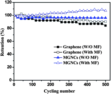
Fig. 10 shows the electrochemical capacitance stability of graphene and its MGNCs with/without an external MF after 500 cycles. It is obvious that the electrode exhibits better cycling performance in the presence of a MF for both graphene and MGNCs. Without a MF, about 84.2% of the initial capacitance can be maintained after 500 cycles. After applying a small MF, 90.2% of initial capacitance is retained, which could be attributed to the improved energy state of the electrons in MF. The MGNCs show even better cycling performance than graphene. The capacitance experiences an initial drop to about 94% within the initial 40 cycles and then is stabilized afterward with 96.1% retention after 500 cycles. The superior cycling performance can be attributed to the structure stability with magnetic NPs extended in the graphene layers to allow the hybrid structure to be more accessible to the electrolyte ions. In the presence of a MF, the cycling performance of the MGNCs is surprisingly improved by 7.1% without degradation after 500 cycles. This unique cycling behavior could be ascribed to the enhanced active surface area during the charge/discharge process. In other words, the external MF enhances the energy state of the electrons and thus increases the electron transfer efficiency at the electrolyte–electrode interface (double layer). The disturbed charging/discharging process helps electrolyte ions to penetrate into the composite structure57 and activates an additional double layer area that was not active in a normal process. Therefore, a gradually increased capacitance performance is observed during cycling.
 | ||
| Fig. 10 Cycling performance of graphene and MGNCs with and W/O MF at the current density of 1.0 A g−1. | ||
4. Conclusions
Fe2O3 nanoparticles have been successfully decorated on the graphene surface via a facile thermal decomposition method. The particle size is observed to be uniformly distributed within the range of 12–30 nm. The NPs are preferentially grown at the defect sites along the graphene edges as directly evidenced by the TEM results. AFM results confirm a particle stacking behavior rather than mono-layer deposition on the graphene sheet. The capacitance performance of the MGNCs is significantly reduced due to the increased internal resistance and thus lowered electron transportation efficiency after decorating an intense loading of the non-conductive Fe2O3 NPs. After locating the electrode in an external magnetic field, the capacitance of graphene is significantly enhanced by 67.1 and 26.8% at the sweeping rates of 2 and 10 mV s−1, respectively. The MGNCs exhibit even larger enhancements by 154.6 and 98.2% at the same sweeping rates of 2 and 10 mV s−1. Both graphene and MGNCs electrodes show satisfactory energy density and power density, especially in the presence of an external magnetic field. Equivalent circuit modeling of the electrochemical impedance spectra reveals a large leakage resistance at the electrode–electrolyte interface due to a relaxation process at low frequency, which was significantly restricted after applying a small magnetic field and thus the capacitor performance was substantially enhanced. These results open a new way to upgrade the current electrochemical capacitors by simply applying an external magnetic field.Acknowledgements
This work is supported by the Research Enhanced Grant (REG) of Lamar University. Partial financial support from NSF – Chemical and Biological Separation under the EAGER program (CBET 11-37441) is kindly acknowledged. We acknowledge the support from the National Science Foundation-Nanoscale Interdisciplinary Research Team and Materials Processing and Manufacturing (CMMI 10-30755) to obtain the DSC and TGA.Notes and references
- K. S. Novoselov, D. Jiang, F. Schedin, T. J. Booth, V. V. Khotkevich, S. V. Morozov and A. K. Geim, Proc. Natl. Acad. Sci. U. S. A., 2005, 102, 10451–10453 CrossRef CAS
.
- Y. Zhang, Y.-W. Tan, H. L. Stormer and P. Kim, Nature, 2005, 438, 201–204 CrossRef CAS
- K. S. Novoselov, A. K. Geim, S. V. Morozov, D. Jiang, Y. Zhang, S. V. Dubonos, I. V. Grigorieva and A. A. Firsov, Science, 2004, 306, 666 CrossRef CAS
- D. A. Abanin, S. V. Morozov, L. A. Ponomarenko, R. V. Gorbachev, A. S. Mayorov, M. I. Katsnelson, K. Watanabe, T. Taniguchi, K. S. Novoselov, L. S. Levitov and A. K. Geim, Science, 2011, 332, 328–330 CrossRef CAS
- J. H. Seol, I. Jo, A. L. Moore, L. Lindsay, Z. H. Aitken, M. T. Pettes, X. Li, Z. Yao, R. Huang, D. Broido, N. Mingo, R. S. Ruoff and L. Shi, Science, 2010, 328, 213–216 CrossRef CAS
- A. Dimiev, D. V. Kosynkin, A. Sinitskii, A. Slesarev, Z. Sun and J. M. Tour, Science, 2011, 331, 1168–1172 CrossRef CAS
- P. Avouris, Nano Lett., 2010, 10, 4285–4294 CrossRef CAS
- V. M. Karpan, G. Giovannetti, P. A. Khomyakov, M. Talanana, A. A. Starikov, M. Zwierzycki, J. van den Brink, G. Brocks and P. J. Kelly, Phys. Rev. Lett., 2007, 99, 176602 CrossRef CAS
- Z. Wei, D. Wang, S. Kim, S.-Y. Kim, Y. Hu, M. K. Yakes, A. R. Laracuente, Z. Dai, S. R. Marder, C. Berger, W. P. King, W. A. de Heer, P. E. Sheehan and E. Riedo, Science, 2010, 328, 1373–1376 CrossRef CAS
- X. Li, W. Cai, J. An, S. Kim, J. Nah, D. Yang, R. Piner, A. Velamakanni, I. Jung, E. Tutuc, S. K. Banerjee, L. Colombo and R. S. Ruoff, Science, 2009, 324, 1312–1314 CrossRef CAS
- Y. Sun, Q. Wu and G. Shi, Energy Environ. Sci., 2011, 4, 1113–1132 CAS
- E. H. Hwang and S. Das Sarma, Phys. Rev. B: Condens. Matter Mater. Phys., 2007, 75, 205418 CrossRef
- M. Jablan, H. Buljan and M. Soljaccaronicacute, Phys. Rev. B: Condens. Matter Mater. Phys., 2009, 80, 245435 CrossRef
- Y. Liang, H. Wang, H. S. Casalongue, Z. Chen and H. Dai, Nano Res., 2010, 3, 701–705 CrossRef CAS
- D. Wang, D. Choi, J. Li, Z. Yang, Z. Nie, R. Kou, D. Hu, C. Wang, L. V. Saraf, J. Zhang, I. A. Aksay and J. Liu, ACS Nano, 2009, 3, 907–914 CrossRef CAS
- S. Guo, S. Dong and E. Wang, ACS Nano, 2009, 4, 547–555 CrossRef
- V. Chandra, J. Park, Y. Chun, J. W. Lee, I.-C. Hwang and K. S. Kim, ACS Nano, 2010, 4, 3979–3986 CrossRef CAS
- J. Zhu, R. Sadu, S. Wei, D. H. Chen, N. Haldolaarachchige, Z. Luo, J. A. Gomes, D. P. Young and Z. Guo, ECS J. Solid State Sci. Technol., 2012, 1, M1–M5 Search PubMed
- J. Zhu, S. Wei, H. Gu, S. B. Rapole, Q. Wang, Z. Luo, N. Haldolaarachchige, D. P. Young and Z. Guo, Environ. Sci. Technol., 2012, 46, 977–985 CrossRef CAS
- S. Pei and H.-M. Cheng, Carbon, 2012, 50, 3210–3228 CrossRef CAS
- M. D. Stoller, S. Park, Y. Zhu, J. An and R. S. Ruoff, Nano Lett., 2008, 8, 3498–3502 CrossRef CAS
- M. D. Stoller, C. W. Magnuson, Y. Zhu, S. Murali, J. W. Suk, R. Piner and R. S. Ruoff, Energy Environ. Sci., 2011, 4, 4685–4689 CAS
- H. Gwon, H.-S. Kim, K. U. Lee, D.-H. Seo, Y. C. Park, Y.-S. Lee, B. T. Ahn and K. Kang, Energy Environ. Sci., 2011, 4, 1277–1283 CAS
- D.-W. Wang, F. Li, J. Zhao, W. Ren, Z.-G. Chen, J. Tan, Z.-S. Wu, I. Gentle, G. Q. Lu and H.-M. Cheng, ACS Nano, 2009, 3, 1745–1752 CrossRef CAS
- J. Xu, K. Wang, S.-Z. Zu, B.-H. Han and Z. Wei, ACS Nano, 2010, 4, 5019–5026 CrossRef CAS
- K. Zhang, L. L. Zhang, X. S. Zhao and J. Wu, Chem. Mater., 2010, 22, 1392–1401 CrossRef CAS
- D. Wei, S. J. Wakeham, T. W. Ng, M. J. Thwaites, H. Brown and P. Beecher, Electrochem. Commun., 2009, 11, 2285–2287 CrossRef CAS
- V. D. Patake, C. D. Lokhande and O. S. Joo, Appl. Surf. Sci., 2009, 255, 4192–4196 CrossRef CAS
- S. Chen, J. Zhu, X. Wu, Q. Han and X. Wang, ACS Nano, 2010, 4, 2822–2830 CrossRef CAS
- A. K. Mishra and S. Ramaprabhu, J. Phys. Chem. C, 2011, 115, 14006–14013 CAS
- D. F. Bartlett, Am. J. Phys., 1990, 58, 1168 CrossRef
- J. Zhu, S. Wei, N. Haldolaarachchige, J. He, D. P. Young and Z. Guo, Nanoscale, 2012, 4, 152–156 RSC
- J. Zhu, Z. Luo, S. Wu, N. Haldolaarachchige, D. P. Young, S. Wei and Z. Guo, J. Mater. Chem., 2012, 22, 835–844 RSC
- W. Y. Kim and K. S. Kim, Nat. Nanotechnol., 2008, 3, 408–412 CrossRef CAS
- A. L. Friedman, J. L. Tedesco, P. M. Campbell, J. C. Culbertson, E. Aifer, F. K. Perkins, R. L. Myers-Ward, J. K. Hite, C. R. Eddy, G. G. Jernigan and D. K. Gaskill, Nano Lett., 2010, 10, 3962–3965 CrossRef CAS
- L. Ji, Z. Tan, T. Kuykendall, E. J. An, Y. Fu, V. Battaglia and Y. Zhang, Energy Environ. Sci., 2011, 4, 3611–3616 CAS
- J. Zhu, H. Gu, Z. Luo, N. Haldolaarachige, D. P. Young, S. Wei and Z. Guo, Langmuir, 2012, 28, 10246–10255 CrossRef CAS
- W. S. Hummers and R. E. Offeman, J. Am. Chem. Soc., 1958, 80, 1339 CrossRef CAS
- N. I. Kovtyukhova, P. J. Ollivier, B. R. Martin, T. E. Mallouk, S. A. Chizhik, E. V. Buzaneva and A. D. Gorchinskiy, Chem. Mater., 1999, 11, 771–778 CrossRef CAS
- X. Wang, S. M. Tabakman and H. Dai, J. Am. Chem. Soc., 2008, 130, 8152–8153 CrossRef CAS
- Y. Lu, S. Bangsaruntip, X. Wang, L. Zhang, Y. Nishi and H. Dai, J. Am. Chem. Soc., 2006, 128, 3518–3519 CrossRef CAS
- D. B. Farmer and R. G. Gordon, Nano Lett., 2006, 6, 699–703 CrossRef CAS
- Y. Lin, D. W. Baggett, J.-W. Kim, E. J. Siochi and J. W. Connell, ACS Appl. Mater. Interfaces, 2011, 3, 1652–1664 CAS
- G. Williams, B. Seger and P. V. Kamat, ACS Nano, 2008, 2, 1487–1491 CrossRef CAS
- J. Yan, T. Wei, Z. Fan, W. Qian, M. Zhang, X. Shen and F. Wei, J. Power Sources, 2010, 195, 3041–3045 CrossRef CAS
- R. B. Rakhi, W. Chen, D. Cha and H. N. Alshareef, J. Mater. Chem., 2011, 21, 16197–16204 RSC
- L. Zhang and G. Shi, J. Phys. Chem. C, 2011, 115, 17206–17212 CAS
- T. Y. Kim, H. W. Lee, M. Stoller, D. R. Dreyer, C. W. Bielawski, R. S. Ruoff and K. S. Suh, ACS Nano, 2011, 5, 436–442 CrossRef CAS
- Electrochemical Supercapacitors: Scientific Fundamentals and Technological Applications, ed. B. E. Conway, Plenum Publishing Co., New York, 1999 Search PubMed
- I. Eremin and A. V. Chubukov, Phys. Rev. B: Condens. Matter Mater. Phys., 2010, 81, 024511 CrossRef
- J. Zang and X. Li, J. Mater. Chem., 2011, 21, 10965–10969 RSC
- P. Simon and Y. Gogotsi, Nat. Mater., 2008, 7, 845–854 CrossRef CAS
- L. L. Zhang and X. S. Zhao, Chem. Soc. Rev., 2009, 38, 2520–2531 RSC
- M. M. Shaijumon, F. S. Ou, L. Ci and P. M. Ajayan, Chem. Commun., 2008, 2373–2375 RSC
- M. Hughes, M. S. P. Shaffer, A. C. Renouf, C. Singh, G. Z. Chen, D. J. Fray and A. H. Windle, Adv. Mater., 2002, 14, 382–385 CrossRef CAS
- J. M. Miller and B. Dunn, Langmuir, 1999, 15, 799–806 CrossRef CAS
- D. Wang, R. Kou, D. Choi, Z. Yang, Z. Nie, J. Li, L. V. Saraf, D. Hu, J. Zhang, G. L. Graff, J. Liu, M. A. Pope and I. A. Aksay, ACS Nano, 2010, 4, 1587–1595 CrossRef CAS
Footnote |
| † Electronic supplementary information (ESI) available. See DOI: 10.1039/c2ee23422j |
| This journal is © The Royal Society of Chemistry 2013 |