Nanocrystalline solar cells with an antimony sulfide solid absorber by atomic layer deposition†
Hannes
Wedemeyer
a,
Jan
Michels
a,
Radoslaw
Chmielowski
b,
Stéphane
Bourdais
b,
Takuma
Muto
b,
Mikio
Sugiura
b,
Gilles
Dennler
b and
Julien
Bachmann
*ac
aUniversity of Hamburg, Departments of Physics and Chemistry, Interdisciplinary Nanoscience Center Hamburg, Sedanstr. 19, D-20146 Hamburg, Germany
bIMRA Europe SAS, Department Energy and the Environment, 220 rue Albert Caquot, BP213, F-06904 Sophia Antipolis Cedex, France
cFriedrich Alexander University Erlangen-Nürnberg, Dept of Chemistry and Pharmacy, Egerlandstr. 1, D-91058 Erlangen, Germany. E-mail: julien.bachmann@chemie.uni-erlangen.de
First published on 18th October 2012
Abstract
Extremely thin absorber solar cells are built in which an Sb2S3 absorber coating is created by atomic layer deposition (ALD). The material is distributed homogeneously along the depth axis and is free of oxide. Under our conditions, an optimal thickness of 10 nm, Sb2S3, yields efficiencies of up to 2.6%.
Broader contextExtremely thin absorber solar cells, or ETA cells, can be described as a type of dye-sensitized photovoltaics in which the molecular light absorber is replaced by a nanometer thick layer of an inorganic solid. ETA systems have the advantages of low material costs and stability, but the best efficiencies reported to date are on the order of 1.5% to 5% only. One hurdle on the way towards a better understanding of the factors determining the efficiency parameters in ETA cells is the often ill-defined geometry. The light-absorbing solid must be infiltrated into a maze of TiO2 nanocrystals, which typically function as electron conductors and provide a high specific surface area. In this work, we deposit a light-absorbing layer of antimony sulfide, Sb2S3, by atomic layer deposition (ALD), a dry thin film method based on well-defined surface chemistry, and demonstrate the advantageous characteristics of ALD in this context: (a) the homogeneous deposition across the whole depth of the nanocrystalline bed, (b) the accurate tuning of the amount deposited, and (c) the absence of unwanted oxide. We reach a maximum efficiency of 2.6% based on colloidal TiO2 nanocrystals, a 9 nanometer thick layer of Sb2S3 by ALD, and CuSCN infiltrated from the solution. |
Extremely thin absorber (ETA) solar cells are photovoltaic structures based on the classic dye-sensitized model in which the electrolyte and the monolayer of adsorbed molecular dye are replaced with solids.1,2 Typically, direct-bandgap semiconductors of the II–VI or V–VI families such as CdSe, In2S3 or Sb2S3 have been used as absorbers, whereas the solid hole conductor CuSCN often serves as the ‘electrolyte’. In fact, ETA cells can also be considered as a particular case of p–i–n heterojunctions, whereby the n-type semiconductor is usually a nanostructured oxide (most prominently TiO2 or ZnO), and charge carriers are generated in the intrinsic layer. Such cells combine the practical advantages of the dye-sensitized model (potentially low material costs, relative flexibility) with a superior stability. The recorded efficiencies of ETA cells currently lie in the range of 1.5% to 5%.3–8
Despite the complex geometry of the electron conducting nanocrystalline TiO2 layer, the absorber must be evenly distributed throughout the structure, either as a thin continuous sheath of homogeneous thickness or as a layer of uniformly arranged nanocrystals between the n- and p-conducting phases. During preparation, the tortuous diffusion paths represent a challenge. Therefore, to date, the absorber has been deposited almost exclusively by wet chemical or electrochemical methods.1–8 These methods are better suited to the infiltration of highly porous systems than ‘dry’ thin film deposition techniques from vaporized or atomized precursors in a vacuum, where mass transport from the gas phase is typically limiting. However, solution methods may not enable one to reach neither the same level of thickness control nor similar purities.9,10 Atomic layer deposition (ALD) essentially combines the best of both worlds, since it relies on two complementary surface reactions that alternate and yield a ‘self-limiting’ growth, thereby circumventing the limitations associated with mass transport. The solid is deposited conformally in a layer by layer fashion, and its thickness linearly depends on the number of reaction cycles carried out and can be defined with nanometer precision.11–14 Thereby, ALD uniquely fits the requirements for creating the inorganic absorber layer in ETA solar cells. Additionally, it has become a mass production method with throughputs on the order of 100 m2 per hour and per tool demonstrated already. ALD can be carried out under atmospheric conditions and with extremely low consumption of chemicals—a major advantage with respect to wet chemical methods based on solvents.15 Despite this, only two very recent examples are to be found for ALD being exploited for this purpose, and the highest power conversion efficiency reported is a modest 0.25%.16,17 The results presented below demonstrate that ALD is applicable to the deposition of a Sb2S3 layer in ‘ETA’ sensitized cells based on nanocrystalline TiO2, and to the accurate tuning of the amount deposited. In this first series of experiments, a maximal efficiency of 2.6% has been achieved.
All preparative steps apart from the coating with Sb2S3 were performed according to previously published procedures.5,18 TiO2 nanocrystals of approximately 100–200 nm size and an active surface area of 16 m2 g−1 (BET adsorption isotherm) were used as electron conductors. They were obtained by sol–gel methods,19 deposited in layers of ∼2 μm thickness onto fluorine-doped SnO2 (FTO) glass slides previously coated with a compact TiO2 film by spray pyrolysis,20 and annealed to 450 °C. Subsequently, the ALD of amorphous antimony sulfide (a-Sb2S3) was performed at 120 °C in a home-made hot-wall reactor from Sb(NMe3) and H2S gas.21–23 A chemically resistant membrane pump MV10C by Vacuubrand was used in the ALD reactor, and unreacted H2S was removed from the exhaust by a bed of Sulfatreat Select HP from MI Swaco. After annealing at 315 °C under N2, a LiSCN treatment was performed, after which the CuSCN hole conductor was infiltrated from iPr2S solution.24 Finally, gold contacts were evaporated, and the cells were characterized electrically in the dark and under one sun after 2 h of irradiation.
We first check that the procedure21,23 for the ALD of a-Sb2S3 adequately coats the highly porous nanocrystalline TiO2 (nc-TiO2) layer conformally. Indeed, a homogeneous distribution of the absorber along the depth axis of the photovoltaic structure is of crucial importance to the function of this type of solar cells. A first indication is given by scanning electron microscopic investigation at the edge of a broken sample: the Sb/Ti ratios calculated from energy-dispersive X-ray (EDX) spectra recorded along the profile vary within a 20% margin. Transmission electron microscopy (TEM) furnishes information of higher spatial resolution. Fig. 1 presents a thin slice of a complete cell the absorber of which was not annealed. An overview of the whole cross-section is presented in high-angle annular dark-field (HAADF) mode in Fig. 1a. Because materials containing heavy elements then appear in light shades of gray, the a-Sb2S3 ALD layer can be observed as a white lining around each dark TiO2 nanocrystal. This layer is found from the top of the sample (where the light gray CuSCN matrix dominates) to its bottom (where the FTO substrate is seen). The fact that Sb2S3 is found at the deepest point of the nanoporous layer proves the ability of the ALD method to reach such difficult areas, in line with the SEM-EDX profile. An excerpt investigated at a higher magnification offers a better contrast (Fig. 1b) and reveals the significant roughness of the a-Sb2S3 sheath. This observation is consistent with the initial report on the ALD reaction used here.21 The 2![[thin space (1/6-em)]](https://www.rsc.org/images/entities/char_2009.gif) :3 stoichiometry of the material and its amorphous nature are also confirmed by TEM-EDX and by the high-resolution micrograph of Fig. 1c, respectively.
:3 stoichiometry of the material and its amorphous nature are also confirmed by TEM-EDX and by the high-resolution micrograph of Fig. 1c, respectively.
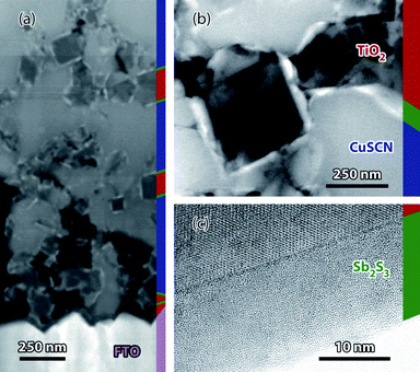 | ||
| Fig. 1 Transmission electron micrographs (Jeol 2100F, 200 kV) of a sample consisting of a-Sb2S3 (150 ALD cycles)/nc-TiO2/FTO layer on glass at three magnification levels. (a) Overview of the cross-section in STEM-HAADF: the thick FTO layer is visible at the bottom, the TiO2 nanocrystals appear dark gray in the CuSCN matrix in lighter gray, and the white linings are the Sb2S3 layer, whereas voids are black. The ALD layer is found throughout the sample. (b) Excerpt taken at a higher magnification. (c) High-resolution micrograph (bright field) showing the amorphous antimony sulfide layer on crystalline TiO2. The various phases are color-coded on a thin stripe at the right edge of each micrograph. | ||
The ALD procedure also enables the experimentalist to control and tune the amount of the absorber deposited. The homogeneously dyed samples obtained immediately after coating the TiO2 nanocrystals with 50, 100, 150, and 200 ALD cycles of a-Sb2S3 are displayed in Fig. 2a. Their diffuse absorption spectra are shown in Fig. 2b. The orange hue and the absorption edge near 600 nm are consistent with the amorphous character of the ALD-Sb2S3 described previously.21 The color also becomes more intense and more saturated with increasing number (N) of ALD cycles, consistent with a linear thickness dependence on N. An ALD growth rate of 0.066 nm per cycle was determined by spectroscopic ellipsometry analysis of a-Sb2S3 layers deposited on flat Si wafers under the same conditions (Fig. 2c), a value similar to that reported.21 With this, the thicknesses deposited range from 3 nm to 13 nm for N = 50 to 200.
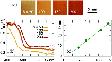 | ||
| Fig. 2 Control of the a-Sb2S3 layer thickness deposited by ALD. (a) Photographs of nc-TiO2 samples after N = 50, 100, 150, and 200 cycles. (b) Absorption spectra of the same samples. For each sample, diffuse transmission and reflectance spectra were recorded with an integrating sphere with the same sample side facing the light source, and the absorption was determined by subtracting the transmitted and reflected intensities from the incident light. (c) The ALD growth rate of 0.66 nm per cycle determined by spectroscopic ellipsometry: the thickness (t) of a-Sb2S3 films on Si wafers vs. the number (N) of ALD cycles performed. | ||
Following ALD, the amorphous absorber layer is crystallized by annealing at 315 °C. The results are displayed in Fig. 3a, which compares the X-ray diffraction patterns obtained before and after the thermal treatment. Immediately after the ALD procedure (thin line), the sample only yields the peaks of anatase TiO2 (red marks) and tetragonal SnO2 (beige, from the FTO). After annealing, the pattern of c-Sb2S3 (green marks) superimposes on this background. None of the reflections expected for Sb2O3 (sky blue ticks) is observed. This is a token of the purity of the sulfide material deposited in ALD, and stands in contrast to the reports of ‘unavoidable’ inclusion of oxygen when the inorganic absorber is deposited from the solution (‘chemical bath deposition’ or CBD).25,26 The crystallization also alters the visual appearance and the optical absorption spectrum of the system, Fig. 3b. The dark brown color of annealed samples is due to a red-shift of the absorption edge from approximately 600 to about 730 nm, in consistency with literature precedents.27–30
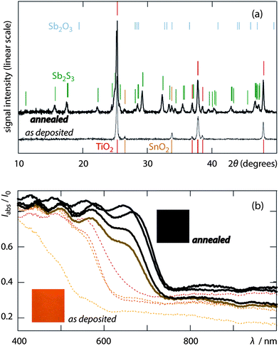 | ||
| Fig. 3 Crystallization of the ALD layer by thermal annealing. (a) X-ray diffraction (XRD) patterns of an Sb2S3 (150 ALD cycles)/nc-TiO2/FTO sample on glass, after the ALD deposition (thin curve) and after annealing (30 min/315 °C/N2, thick curve). The former only displays the peaks of TiO2 (anatase, red) and SnO2 (cassiterite, beige), whereas Sb2S3 is amorphous. The latter exhibits strong signals for crystalline Sb2S3 (stibnite, forest green); no Sb2O3 (valentinite, sky blue) is observed. (b) Diffuse absorption spectra before and after annealing (dotted and thick lines, respectively, with N encoded in increasingly dark shades): the absorption edge red-shifts by >100 nm; insets are photographs for N = 150. | ||
Not only the crystallinity of the deposit changes upon annealing: the high mobility of Sb2S3, already noted in the past,23 causes its morphology to be affected, as well. The evolution of the microstructure on the top side of the nc-TiO2 film upon ALD and then annealing is presented in Fig. 4a. The sharp edges of the TiO2 crystals initially visible are rounded off by the amorphous ALD deposit, as expected from a conformal coating. After annealing, some of the underlying edges have reappeared, and crystallites of less well defined shape than the TiO2 crystals can be attributed to Sb2S3. A clearer picture is afforded by transmission electron microscopy. A solar cell obtained after annealing, CuSCN infiltration and Au deposition was prepared for TEM and investigated in HAADF mode (Fig. 4b). The low-magnification image on the left looks similar to Fig. 2a: the FTO layer appears at the bottom, most of the area is occupied by the nc-TiO2/c-Sb2S3/CuSCN composite, and the homogeneous CuSCN overlayer is found near the top. In the active nc-TiO2/c-Sb2S3/CuSCN section, the electron and hole conducting phases can be distinguished in two different shades of gray, and the thin ALD coatings are visible in white around the TiO2 grains, homogeneously distributed from top to bottom. Some cavities appear black, which the CuSCN solution was presumably not able to infiltrate.
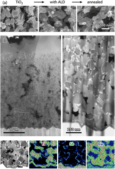 | ||
| Fig. 4 Microstructure of ETA solar cells based on Sb2S3 by ALD. (a) Changes observed by SEM (top view) upon ALD and annealing. (b) STEM-HAADF micrographs of a functional solar cell in the cross-section at two distinct magnifications. (c) Distribution of the phases TiO2, Sb2S3, and CuSCN near the FTO-side of the solar cell (EDX mappings of the elements Ti, Sb, and Cu; the signals of the elements Sn and Sb overlap). | ||
A region in the vicinity of the FTO film is magnified on the right side of Fig. 4b. Here and with the help of EDX mappings (Fig. 4c), the individual phases can be distinguished unambiguously. The TiO2 crystals are embedded in a CuSCN matrix, whereas the compact TiO2 layer prevents the direct contact between CuSCN and FTO. However, the ALD coating is not conformal, in contrast to the amorphous case (Fig. 2b) and in accordance with what could be gathered from the third micrograph of Fig. 4a. The ALD layer loses its continuity upon crystallization, so that in the functional solar cell it only covers a certain fraction of the TiO2 surfaces, leaving some TiO2 surfaces in direct contact with CuSCN.
Despite this, the samples of 50 mm2 area show the typical rectifying behavior of a diode in the dark (red curve of Fig. 5a), as well as a photovoltaic response when irradiated under 1 sun (AM1.5, green curve). The sample prepared with 150 ALD cycles delivers up to 0.47 V, a value significantly lower than the potential difference between the TiO2 conduction band edge and the CuSCN valence band edge (for which values from−4.0 to −4.3 V and from −5.0 to −5.3 V can be found in the literature, respectively),5,31–34 but in line with the state of the art in the TiO2/Sb2S3/CuSCN system.18 Its short-circuit current density is lower than that reported recently.18 The spectrum for the incident photon to current efficiency (IPCE), shown in Fig. 5b, displays an onset near 730 nm, in a manner that mirrors the absorption curve of Fig. 3b.
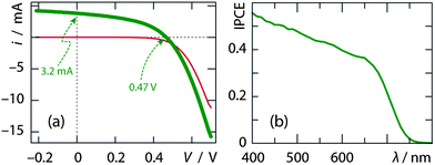 | ||
| Fig. 5 Photovoltaic characterization of a solar cell based on 150 cycles of Sb2S3 ALD (0.50 cm2) after 2 hours of irradiation. (a) Electrical current–voltage curves taken in the dark (thin red line) and under AM1.5 irradiation (one sun, thick green). Both of them were recorded after 2 hours of irradiation. The values measured for iSC and VOC are indicated. (b) Incident photon to current efficiency spectrum in the visible range. | ||
The photovoltaic parameters of four 50 mm2 samples differing by the number (N) of Sb2S3 ALD cycles performed (corresponding to thicknesses of 7, 10, and 13 nm) and the crystallinity of the layer (with or without annealing) are summarized in Table 1. The comparison between the first two samples exemplifies the effect of annealing eloquently. The poor optical and electric properties of a-Sb2S3 essentially withdraw the photovoltaic character of the structure. If the absorber layer is crystalline, then its thickness determines the amount of light absorbed and converted, and thereby the current, without significantly influencing the open-circuit potential. Beyond a certain amount of inorganic absorber (10 nm in our geometry), the current levels off as the absorption has approximately reached unity over the spectrum of c-Sb2S3.
| Absorber state | A/mm2 | N | V OC/V | J SC/mA cm−2 | FF | η |
|---|---|---|---|---|---|---|
| A | 50 | 100 | 0.14 | 0.01 | 0.35 | 0.0003% |
| C | 50 | 100 | 0.41 | 3.2 | 0.41 | 0.53% |
| C | 50 | 150 | 0.47 | 6.4 | 0.46 | 1.4% |
| C | 50 | 200 | 0.47 | 6.3 | 0.44 | 1.3% |
| C | 7 | 150 | 0.49 | 11.6 | 0.48 | 2.6% |
We investigated the homogeneity of our samples by characterizing smaller cells of only 7 mm2 area cut from the larger ones. The spread of values obtained from these small samples for the photovoltaic parameters is very large. For the case of N = 150 Sb2S3 ALD cycles, efficiencies range from 0 to 2.6% for various devices, whereas for each of them the photovoltaic parameters are reproducible. Thus, the photovoltaic system nc-TiO2/ALD-Sb2S3/CuSCN is intrinsically more efficient than the data reported above indicate, and is limited by weak spots rather than by fundamental physics. Based on the observation of large CuSCN-free gaps in our cross-sectional TEM investigations, we consider that the imperfect CuSCN impregnation from the solution likely causes the weak spots.
Conclusions
Taken together, our results demonstrate the validity of atomic layer deposition for creating extremely thin layers of a solid absorber in the preparation of nanocrystalline solar cells with >2% efficiency. This value is among the largest reported for ETA cells but sets no new record. However, ALD is advantageous in several ways in this field. Indeed, the ALD material is free of oxide and can be deposited in homogeneous thickness across the depth of the porous layer of nanocrystalline TiO2, in an amount controlled directly by the number of ALD cycles performed. This property is particularly crucial for studying the influence of the absorber thickness on the photovoltaic parameters of the structure. In the geometry chosen here, a thickness of approximately 10 nm is found as optimum. The crystallization of Sb2S3 upon thermal treatment disturbs the continuity of the ALD film, yet the efficiencies obtained with this limitation are encouraging. We note that our system does not rely upon rare elements.At this point, it seems that structural imperfections in the p-CuSCN deposited by a wet chemical method limit the overall photovoltaic yield. This work will be pursued with the goals of optimizing the infiltration of the hole-conducting phase, then minimizing the recombination of photogenerated charge carriers at the interfaces. We will then be able to explore the influence of the geometric parameters that can be varied in this system.
Acknowledgements
We thank Renbin Yang for a preliminary ALD coating and Kornelius Nielsch for access to a spectroscopic ellipsometer.Notes and references
- K. Tennakone, G. R. R. A. Kumara, I. R. M. Kottegoda, V. P. S. Perera and G. M. L. P. Aponsu, J. Phys. D: Appl. Phys., 1998, 31, 2326 CrossRef CAS.
- I. Kaiser, K. Ernst, C.-H. Fischer, R. Könenkamp, C. Rost, I. Sieber and M. C. Lux-Steiner, Sol. Energy Mater. Sol. Cells, 2001, 67, 89 CrossRef CAS.
- C. Lévy-Clément, R. Tena-Zaera, M. A. Ryan, A. Katty and G. Hodes, Adv. Mater., 2005, 17, 1512 CrossRef.
- A. Belaidi, T. Dittrich, D. Kieven, J. Tornow, K. Schwarzburg and M. C. Lux-Steiner, Phys. Status Solidi RRL, 2008, 2, 172 CrossRef CAS.
- G. Larramona, C. Choné, A. Jacob, D. Sakakura, B. Delatouche, D. Péré, X. Cieren, M. Nagino and R. Bayón, Chem. Mater., 2006, 18, 1688 CrossRef CAS.
- Y. Itzhaik, O. Niitsoo, M. Page and G. Hodes, J. Phys. Chem. C, 2009, 113, 4254 CAS.
- J. A. Chang, J. H. Rhee, S. H. Im, Y. H. Lee, H. Kim, S. I. Seok, M. K. Nazeeruddin and M. Grätzel, Nano Lett., 2010, 10, 2609 CrossRef CAS.
- M. Krunks, E. Kärber, A. Katerski, K. Otto, I. Oja Acik, T. Dedova and A. Mere, Sol. Energy Mater. Sol. Cells, 2010, 94, 1191 CrossRef CAS.
- D. Hiller, R. Zierold, J. Bachmann, M. Alexe, Y. Yang, J. W. Gerlach, A. Stesmans, M. Jivanescu, U. Müller, J. Vogt, H. Hilmer, P. Löper, M. Künle, F. Munnik, K. Nielsch and M. Zacharias, J. Appl. Phys., 2010, 107, 064314 CrossRef.
- T. Hirvikorpi, M. Vähä-Nissi, A. Harlin and M. Karppinen, Thin Solid Films, 2010, 518, 5463 CrossRef CAS.
- R. L. Puurunen, J. Appl. Phys., 2005, 97, 121301 CrossRef.
- M. Knez, K. Nielsch and L. Niinistö, Adv. Mater., 2007, 19, 3425 CrossRef CAS.
- S. M. George, Chem. Rev., 2010, 110, 111 CrossRef CAS.
- J. Bachmann, J. Escrig, K. Pitzschel, J. M. Montero Moreno, J. Jing, D. Görlitz, D. Altbir and K. Nielsch, J. Appl. Phys., 2009, 105, 07B521 CrossRef.
- Specifications excerpted from the technical datasheet provided by Rena GmbH, Gütenbach (Germany), for the product SoLayTec InPassion ALD 3600: http://de.rena.com/fileadmin/img/Produkte/200_Solartechnik/220_Inline/2303_SoLayTec/RENA_DB_SoLayTec_20120913-final.pdf.
- T. P. Brennan, P. Ardalan, H.-B.-R. Lee, J. R. Bakke, I.-K. Ding, M. D. McGehee and S. F. Bent, Adv. Energy Mater., 2011, 1, 1169 CrossRef CAS.
- S. K. Sarkar, J. Y. Kim, D. N. Goldstein, N. R. Neale, K. Zhu, C. M. Elliot, A. J. Frank and S. M. George, J. Phys. Chem. C, 2010, 114, 8032 CAS.
- S. Nezu, G. Larramona, C. Choné, A. Jacob, B. Delatouche, D. Péré and C. Moisan, J. Phys. Chem. C, 2010, 114, 6854 CAS.
- L. Kavan and M. Grätzel, Electrochim. Acta, 1995, 40, 643 CrossRef CAS.
- C. J. Barbé, F. Arendse, P. Comte, M. Jirousek, F. Lenzmann, V. Shklover and M. Grätzel, J. Am. Ceram. Soc., 1997, 80, 3157 CrossRef.
- Caution : hydrogen sulfide is highly toxic!.
- R. B. Yang, J. Bachmann, M. Reiche, J. W. Gerlach, U. Gösele and K. Nielsch, Chem. Mater., 2009, 21, 2586 CrossRef CAS.
- R. B. Yang, N. Zakharov, O. Moutanabbir, K. Scheerschmidt, L.-M. Wu, U. Gösele, J. Bachmann and K. Nielsch, J. Am. Chem. Soc., 2010, 132, 7592 CrossRef CAS.
- B. O'Regan, F. Lenzmann, R. Muis and J. Wienke, Chem. Mater., 2002, 14, 5023 CrossRef CAS.
- C. D. Lokhande, B. R. Sankapal, R. S. Mane, H. M. Pathan, M. Muller, M. Giersig and V. Ganesan, Appl. Surf. Sci., 2002, 193, 1 CrossRef CAS.
- B. Krishnan, A. Arato, E. Cardenas, T. K. Das Roy and G. A. Castillo, Appl. Surf. Sci., 2008, 254, 3200 CrossRef CAS.
- I. Grozdanov, M. Ristov, G. j. Sinadinovski and M. Mitreski, J. Non-Cryst. Solids, 1994, 175, 77 CrossRef CAS.
- N. Tigau, Cryst. Res. Technol., 2007, 42, 281 CrossRef CAS.
- M. Y. Versavel and J. A. Haber, Thin Solid Films, 2007, 515, 7171 CrossRef CAS.
- B. Krishnan, A. Arato, E. Cardenas, T. K. Das Roy and G. A. Castillo, Appl. Surf. Sci., 2008, 254, 3200 CrossRef CAS.
- W. H. Strehlow and E. L. Cook, J. Phys. Chem. Ref. Data, 1973, 2, 163 CrossRef CAS.
- B. C. O'Regan and F. Lenzmann, J. Phys. Chem. B, 2004, 108, 4342 CrossRef CAS.
- C. A. Melendres, T. J. O'Leary and J. Solis, Electrochim. Acta, 1991, 36, 505 CrossRef CAS.
- Y. Xu and M. A. A. Schoonen, Am. Mineral., 2000, 85, 543 CAS.
Footnote |
| † Electronic supplementary information (ESI) available. See DOI: 10.1039/c2ee23205g |
| This journal is © The Royal Society of Chemistry 2013 |