Enhancing solar cell efficiency: the search for luminescent materials as spectral converters
Xiaoyong
Huang
a,
Sanyang
Han
a,
Wei
Huang
*bc and
Xiaogang
Liu
*ad
aDepartment of Chemistry, Faculty of Science, National University of Singapore, 3 Science Drive 3, 117543, Singapore. E-mail: chmlx@nus.edu.sg
bSingapore-Jiangsu Joint Research Center for Organic/Bio-electronics and Information Displays and Institute of Advanced Materials, Nanjing University of Technology, Nanjing 211816, China. E-mail: wei-huang@njut.edu.cn
cKey Laboratory for Organic Electronics and Information Displays and Institute of Advanced Materials, Nanjing University of Posts and Telecommunications, Nanjing 210046, China. E-mail: iamwhuang@njupt.edu.cn
dInstitute of Materials Research and Engineering, Agency for Science, Technology and Research, 3 Research Link, 117602, Singapore
First published on 16th October 2012
Abstract
Photovoltaic (PV) technologies for solar energy conversion represent promising routes to green and renewable energy generation. Despite relevant PV technologies being available for more than half a century, the production of solar energy remains costly, largely owing to low power conversion efficiencies of solar cells. The main difficulty in improving the efficiency of PV energy conversion lies in the spectral mismatch between the energy distribution of photons in the incident solar spectrum and the bandgap of a semiconductor material. In recent years, luminescent materials, which are capable of converting a broad spectrum of light into photons of a particular wavelength, have been synthesized and used to minimize the losses in the solar-cell-based energy conversion process. In this review, we will survey recent progress in the development of spectral converters, with a particular emphasis on lanthanide-based upconversion, quantum-cutting and down-shifting materials, for PV applications. In addition, we will also present technical challenges that arise in developing cost-effective high-performance solar cells based on these luminescent materials.
 Xiaoyong Huang | Xiaoyong Huang was born in Jiangxi, China. He obtained his BE degree from China University of Geosciences (Beijing) in 2004 and his MS degree from Institute of Geochemistry, Chinese Academy of Sciences in 2007. Subsequently, he completed his PhD (2011) in the field of lanthanide-ion-doped quantum cutting and upconversion phosphors for photovoltaic applications under the supervision of Prof. Qinyuan Zhang at South China University of Technology. He is currently working as a postdoctoral research fellow in the group of Prof. Xiaogang Liu at the National University of Singapore. His present research focuses on optical spectroscopy and application of luminescent nanomaterials. |
 Sanyang Han | Sanyang Han was born in Hubei, China. He received his BS (2007) and MS (2010) degrees in chemistry from Soochow University. He is currently pursuing a PhD degree under the supervision of Prof. Xiaogang Liu in the Department of Chemistry at the National University of Singapore. His research interest focuses on development of novel lanthanide-doped luminescent nanomaterials. |
 Wei Huang | Wei Huang received his BSc, MSc, and PhD degrees in chemistry from Peking University in 1983, 1988, and 1992, respectively. In 1993, he began his postdoctoral research with the Chemistry Department at National University of Singapore, where he participated in the founding of the Institute of Materials Research and Engineering. In 2001, he became a chair professor at Fudan University, where he founded and chaired the Institute of Advanced Materials. In June 2006, he was appointed as the Deputy President of Nanjing University of Posts and Telecommunications, where he initiated the Institute of Advanced Materials and the Key Laboratory for Organic Electronics and Information Displays. In July 2012, he was appointed as the President of Nanjing University of Technology. He is an academician of the Chinese Academy of Sciences. His research interests include organic opto-electronics, nanomaterials, polymer chemistry, plastic electronics, and bioelectronics. |
 Xiaogang Liu | Xiaogang Liu was born in Jiangxi, China. He earned his BE degree (1996) in Chemical Engineering from Beijing Technology and Business University. He received his MS degree (1999) in chemistry from East Carolina University under the direction of Prof. John Sibert and completed his PhD (2004) at Northwestern University under the supervision of Prof. Chad Mirkin. He then became a postdoctoral fellow in the group of Prof. Francesco Stellacci at MIT. He joined the faculty of the National University of Singapore in 2006. He holds a joint appointment with the Institute of Materials Research and Engineering, Agency for Science, Technology and Research. His interests include lanthanide-doped optical nanomaterials, supramolecular chemistry, and surface science for catalysis, sensors and biomedical applications. |
1. Introduction
Sunlight is a free and, in many parts of the world, abundant source of energy that can be captured by new technologies and transformed into electricity.1,2 It has been reported that sunlight that reaches the Earth's surface delivers 10![[thin space (1/6-em)]](https://www.rsc.org/images/entities/char_2009.gif) 000 times more energy than what we consume.3 As a result, the use of solar energy is expected to have the potential to meet a large portion of future energy consumption requirements. Despite significant development of the photovoltaic (PV) industry over the past decades, the efficient and cost-effective conversion of solar energy into electricity through PV cells remains a daunting task.4–6 Current annual solar energy usage is well below 1% of total energy consumption, while fossil fuels account for over 90% of the energy consumption. Before the large-scale use of solar energy, more efficient PV systems at reduced costs must be developed.7–20
000 times more energy than what we consume.3 As a result, the use of solar energy is expected to have the potential to meet a large portion of future energy consumption requirements. Despite significant development of the photovoltaic (PV) industry over the past decades, the efficient and cost-effective conversion of solar energy into electricity through PV cells remains a daunting task.4–6 Current annual solar energy usage is well below 1% of total energy consumption, while fossil fuels account for over 90% of the energy consumption. Before the large-scale use of solar energy, more efficient PV systems at reduced costs must be developed.7–20
A major problem limiting the conversion efficiency of PV cells is their insensitivity to a full solar spectrum. The spectral distribution of sunlight at Air Mass 1.5 global (AM 1.5G) consists of photons with wide wavelengths ranging from ultraviolet to infrared (280–2500 nm, 0.5–4.4 eV), but current PV cells only utilize a relatively small fraction of the solar photons (Fig. 1).21 This is attributed to the fact that each PV material responds to a narrow range of solar photons with energy matching the characteristic bandgap of the material. In principle, only photons with energy higher than the bandgap are absorbed, but the excess energy is not effectively used and released as heat. The thermalization of photon energies exceeding the bandgap and non-absorption of photons with energy less than the bandgap amount to the loss of approximately 50% of the incident solar energy in silicon-based solar cell conversion to electricity. Notably, the theoretical maximum level of efficiency for crystalline silicon (c-Si) with a bandgap energy (Eg) of 1.1 eV is approximately 31% or 41%, depending on the concentration ratio, as defined by the Shockley–Queisser limit.22
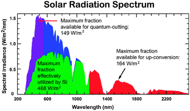 | ||
| Fig. 1 AM 1.5G spectrum showing the fraction (highlighted in green) absorbed by a typical silicon-based PV cell and the spectral regions that can be utilized through quantum-cutting and upconversion processes (highlighted in purple and red, respectively). (Adapted with permission from ref. 21. Copyright 2007, Elsevier B.V.) | ||
The inherent thermalization and non-absorption losses can be minimized using luminescent materials as spectral converters. The approach, termed the third-generation solar photon conversion, involves the incorporation of a passive luminescent layer into PV cells.23–28 An important aspect of using this technology is that spectral converters are readily applicable to existing solar cells with few changes as the spectral converters and solar cells can be optimized independently.
To increase the efficiency of single-junction solar cells, three luminescence processes including upconversion, quantum-cutting, and down-shifting are currently explored for developing efficient PV devices. Trivalent lanthanide ions are the prime candidates to achieve efficient spectral conversion because of their rich energy-level structure (known as the Dieke diagram) that allows for facile photon management.29–31
Upconversion of sub-bandgap light is exploited to reduce non-absorption energy losses. The limiting efficiency of a solar cell, equipped with an upconverter, has recently been discussed by Trupke et al.32 using a detailed balance model. The system under investigation consists of a bifacial single-junction solar cell with an upconverting layer located at the rear of the solar panel (Fig. 2). The upconverter transforms two (or more) transmitted sub-bandgap photons into one usable above-bandgap photon, which is subsequently absorbed by the solar cell to generate electron–hole pairs. The maximum efficiency was calculated to be 47.6% for non-concentrated light.
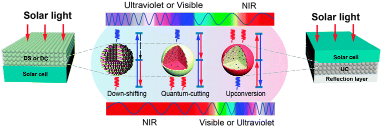 | ||
| Fig. 2 Spectral conversion design for PV applications involving down-shifting (DS), quantum-cutting (QC), and upconversion (UC) luminescent materials. In a typical down-shifting process, upon excitation with a high-energy photon, nonradiative relaxation takes place followed by radiative relaxation, thereby resulting in the emission of a lower-energy photon. In contrast, two-step radiative relaxation occurs in the quantum-cutting process upon excitation with a high-energy photon, leading to the emission of two (or more) lower-energy photons. The upconversion process can convert two (or more) incident low-energy photons into a single higher-energy photon. Both down-shifting and quantum-cutting processes are able to make effective use of the high-energy portion of the solar spectrum, but with dramatically different quantum efficiency. The theoretical quantum efficiency for down-shifting is always less than 100%, whereas it exceeds 100% for quantum-cutting. Note that the down-shifting and quantum-cutting materials are generally placed on the front surface of a monofacial solar cell, allowing the downconverted photons to be absorbed by the solar cell. The upconversion material is typically placed in between a bifacial solar cell and a light-reflection layer to harvest the sub-bandgap spectrum of sunlight. | ||
Quantum-cutting through downconversion is able to split one incident high-energy photon into two (or more) lower-energy photons with a conversion efficiency higher than 100%.33 This process could minimize the energy loss caused by thermalization of hot charge carriers after the absorption of high-energy photons, if the downconverted photons can be absorbed by solar cells. As a result, the photocurrent of the device can be doubled. A recent quantum-cutting model proposed by Trupke et al.34 showed that a solar cell (Eg = 1.1 eV), modified with a downconverting layer on the front surface, can achieve a conversion efficiency of up to 38.6% (Fig. 2).
Down-shifting is a single photon process that involves transformation of one absorbed high-energy photon into one lower-energy photon. This process obeys the Stokes Law with wavelength change known as the Stokes shift. Down-shifting is similar to quantum-cutting, but its conversion efficiency does not exceed 100%. Despite this disadvantage, down-shifting can still be useful for improving PV efficiency by shifting short-wavelength sunlight (usually ultraviolet and blue) to the longer-wavelength region where the spectral response of the solar cell is more sensitive (Fig. 2). Until now, two main classes of down-shifting-based PV devices have been investigated: a luminescent solar concentrator and a planar down-shifting layer. Lanthanide-doped phosphors and glasses, semiconductor quantum dots (QDs) and organolanthanide complexes have been thoroughly explored as potential wavelength-shifting materials.
This review focuses on the importance, development, and implementation of lanthanide-doped luminescent materials for modern PV applications. We begin by describing fundamental aspects central to rational design of solar cells followed by discussing the operating principles of lanthanide-doped upconversion materials as spectral converters to reduce the transmission loss of sub-bandgap light. Furthermore, an overview of the state-of-art near-infrared (NIR) quantum-cutting using a single Ho3+ ion and Ln3+–Yb3+ (Ln = Tb, Tm, Pr, Er, Nd, Ho, and Dy) pairs for c-Si solar cells is presented. The underlying energy transfer (ET) mechanisms are then discussed. The attempts to sensitize Ln3+–Yb3+ couples using ion species (Ce3+, Eu2+, Yb2+, and Bi3+) in different host lattices are subsequently described. We also highlight the topic of multiple exciton generation (MEG) in QDs to reflect an important parallel development promising for solar energy conversion. Finally, we discuss the advances toward realizing spectral conversion by utilizing planar down-shifting layers composed of phosphors, QDs and organolanthanide complexes as fluorophores. Selected examples of recent experimental results will be presented.
2. Fundamental aspects of solar cell design
2.1 Solar cells
Solar cells are typically composed of special light-absorbing semiconducting materials.35 When sunlight falls on a solar cell, the photons activate the electrons in the cell and promote them into a higher energy conduction band. Those electrons can then be harnessed to create electric current. To produce a solar cell, the semiconductor is doped with either positive charge carriers (p-type) or negative charge carriers (n-type). If two differently doped semiconductor layers are combined, then a so-called p–n junction results on the boundary of the layers. The conversion efficiency of solar energy is perhaps the most significant parameter that determines the performance of a PV device. For any traditional single p–n junction solar cell, the bandgap energy of the semiconductor from which the solar cell is fabricated places a fundamental upper limit on its conversion efficiency. Currently, solar cells based on crystalline, polycrystalline and amorphous silicon represent more than 90% of the world production.36 The use of c-Si enables PV devices to achieve a maximum conversion efficiency of 25%.37The c-Si solar cells work most efficiently in the 950–1100 nm spectral region, but they show very low spectral response to the short-wavelength sunlight (Fig. 3). Therefore, ideal quantum-cutting and down-shifting luminescent materials for c-Si solar cells should convert the high-energy (usually ultraviolet–blue) light into the NIR emission around 1000 nm, while the most desirable upconverters for c-Si solar cells are able to absorb light above 1100 nm and convert it into emission around 1000 nm. In principle, an upconverter for c-Si solar cells should satisfy the following requirements: (i) the excitation range longer than 1100 nm (E < 1.12 eV); (ii) the emission range shorter than 1100 nm; (iii) good response under low-intensity excitation (in the range of 10–100 W m−2); and (iv) high conversion efficiency and high transparency toward the upconverted light. Compared to conventional c-Si solar cells, wide bandgap solar cells would benefit much more from incorporation of an upconverting layer due to the dominant transmission losses. The wide bandgap solar cells, including GaAs, amorphous Si, dye-sensitized and organic solar cells, can work well in the visible region, but their absorption is generally limited to a maximum wavelength of ∼900 nm (Fig. 4).38 For example, in an ideal single-junction solar cell with a bandgap of 1.7 eV, approximately 49% of the incoming solar energy is lost because it cannot be absorbed by the solar cell. An ideal upconverter for PV applications would convert incident sub-bandgap sunlight into monochromatic above-bandgap light where solar cells have their optimum spectral response.
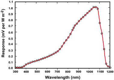 | ||
| Fig. 3 Normalized spectral response of a typical c-Si solar cell pyranometer (courtesy of Apogee Instruments, Inc., 2008). The c-Si is an indirect bandgap semiconductor so there is not a sharp cut off at the wavelength corresponding to the bandgap (Eg = 1.12 eV). | ||
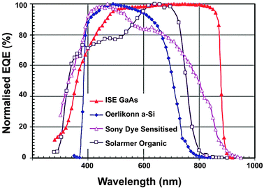 | ||
| Fig. 4 Normalized external quantum efficiency (EQE) spectra for several wide bandgap PV cells. (Reprinted with permission from ref. 38. Copyright 2010, John Wiley & Sons, Ltd.) | ||
2.2 Luminescence
Luminescence generally refers to the emission of light by a material after it has absorbed energy.39 The term ‘luminescence’ was introduced in 1888 by Wiedemann.40 Luminescence can be generated from different types of energetic sources, including electromagnetic radiations, electric fields, X-rays, and charged particles from radioactive decay. Depending upon the nature of the excitation source, luminescence can be subdivided into several categories that are generally indicated by a prefix. In the case of photo-excitation, this luminescence is called photoluminescence. In this review, we will focus on photoluminescence-based spectral conversion approaches for PV applications. Fluorescence and phosphorescence are two major forms of photoluminescence extensively investigated in modern research. They are distinguishable from the decay time (τ). Fluorescence has a short time lapse (τ < 10 ms) after the excitation source is removed, while phosphorescence has a much longer decay time (τ > 0.1 s).40 Inorganic solids that give rise to luminescence are called phosphors or, lately, luminescent materials.41,42 Luminescent materials generally require a host crystalline structure that constitutes the bulk of the phosphors. The characteristic luminescence properties are obtained by doping the host material with relatively small amounts of foreign ions. The luminescence of inorganic solids can be roughly classified into two mechanisms: luminescence of localized centers or activators (Fig. 5a and b) and luminescence of semiconductors through band-to-band excitation (Fig. 5c). To induce luminescence from an activator without efficient absorption for the available excitation energy, a sensitizer ion is often incorporated into the host material to transfer its excitation energy to the activator. The emission color can be readily adjusted by varying the dopant concentration or composition without changing the host lattice. Notably, a number of lanthanide activators show emission spectra with spectral positions that are hardly influenced by their chemical environment.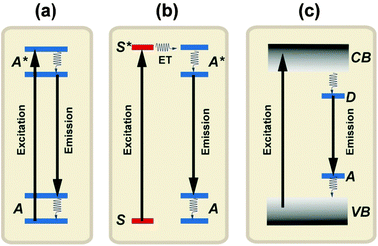 | ||
| Fig. 5 Luminescence in inorganic solids. (a) Emission from a luminescence activator upon excitation. (b) Sensitized emission from an activator through energy transfer from a sensitizer to the activator upon excitation of the sensitizer. (c) Emission from a semiconductor after band-to-band excitation. A and A* represent the ground and excited states of the activator, respectively. S and S* represent the ground and excited states of the sensitizer, respectively. VB and CB represent the valence and conduction bands of the semiconductor, while D and A represent the donor and acceptor energy levels, respectively. | ||
The conversion efficiency of a phosphor, usually expressed as either a quantum efficiency or an energy efficiency, is an important consideration in practical applications. The quantum efficiency (or quantum yield) is defined as the fraction of the input photons contributing to the desired optical process.43,44 In contrast, the energy efficiency is the ratio of the output power to the input power. In a luminescence process, the excited state decays by a combination of radiative and nonradiative processes, and the relative rate of these processes determines the quantum efficiency. Radiative decay describes molecular deexcitation processes accompanied by photon emission. Molecules in the excited states can also relax by nonradiative processes where excitation energy is not converted into photons but is dissipated by thermal processes such as vibrational relaxation and collisional quenching. Let kr and knr be the radiative and nonradiative decay rates, respectively, and N be the population density of luminescence activators in the excited state. The temporal evolution of the excited state can be described by:
 | (1) |
 | (2) |
 | (3) |
2.3 Lanthanide ions
The lanthanide elements, characterized by the progressive filling of the 4f orbitals, are a family of 15 chemically similar elements from lanthanum (La) to lutetium (Lu). The term ‘rare earth’ is applied to lanthanide elements and also to yttrium (Y), which is found in nature always along with the lanthanides. The lanthanides, essentially existing in their most stable oxidation state as trivalent ions (Ln3+), are extensively investigated for their optical properties.47–55 The lanthanide ions feature an electron configuration of 4fn (0 < n < 14) and the arrangements of electrons within this configuration are substantially diverse. This results in a fairly large number of energy levels.56 Most of the fascinating optical properties, such as photon upconversion emission, of lanthanide ions can be ascribed to the electron transitions within the 4fn configuration (Table 1). Most lanthanide ions generally show sharp line spectra, much narrower and more distinct than those for transition metal ions. The spectra are associated with weak f–f electronic transitions. The narrow spectral bands indicate that the f-orbitals have a smaller radial extension than the outer 5s and 5p orbitals, thus leading to smaller electron–phonon coupling strengths and a lower susceptibility to crystal-field and exchange perturbations.| Ln | Ground state | Excited state | Final state | Emission wavelength (nm) | Energy (cm−1) | Intensity | Remarks |
|---|---|---|---|---|---|---|---|
| Pr | 3H4 | 3P2 → | 3H4 | 440 | 22727 |
Weak | QC |
| 3P1 → | 3H4 | 470 | 21277 |
Weak | QC | ||
| 1G4 | 872 | 11468 |
Medium | QC | |||
| 3P0 → | 3H4 | 480 | 20833 |
Strong | UC and QC | ||
| 3H5 | 545 | 18349 |
Weak | UC and QC | |||
| 3H6 | 606 | 16502 |
Medium | UC and QC | |||
| 3F2 | 640 | 15625 |
Weak | UC and QC | |||
| 1D2 → | 3F4 | 1037 | 9643 | Medium | QC | ||
| Nd | 4I9/2 | 4D3/2 → | 4I9/2 | 355 | 28169 |
Weak | UC and QC |
| 2P3/2 → | 4I9/2 | 380 | 26316 |
Weak | UC and QC | ||
| 4I11/2 | 410 | 24390 |
Strong | UC and QC | |||
| 4I13/2 | 452 | 22124 |
Strong | UC and QC | |||
| 4G7/2 → | 4I9/2 | 545 | 18349 |
Weak to strong | UC and QC | ||
| 4I11/2 | 587 | 17036 |
Weak to strong | UC and QC | |||
| 4I13/2 | 655 | 15267 |
Weak to strong | UC and QC | |||
| 4F3/2 → | 4I9/2 | 886 | 11287 |
Weak to strong | QC and DS | ||
| 4I11/2 | 1064 | 9399 | Strong | QC and DS | |||
| 4I13/2 | 1340 | 7463 | Weak | QC and DS | |||
| Sm | 6H5/2 | 4G5/2 → | 6H5/2 | 564 | 17730 |
Medium | DS |
| 6H7/2 | 601 | 16639 |
Strong | DS | |||
| 6H9/2 | 644 | 15528 |
Medium | DS | |||
| Eu | 7F0 | 5D0 → | 7F0,1,2,3,4 | 570–720 | 13889–17544 |
Strong | UC and DS |
| Tb | 7F6 | 5D4 → | 7F6,5,4,3 | 480–650 | 15385–20833 |
Strong | UC, QC and DS |
| Dy | 6H15/2 | 4F9/2 → | 6H15/2 | 486 | 20576 |
Medium | QC and DS |
| 6H13/2 | 575 | 17391 |
Strong | QC and DS | |||
| 6H11/2 | 664 | 15060 |
Weak | QC and DS | |||
| Ho | 5I8 | 5S2, 5F4 → | 5I8 | 540 | 18519 |
Strong | UC and QC |
| 5I7 | 749 | 13351 |
Weak | UC and QC | |||
| 5I6 | 1012 | 9881 | Weak | QC | |||
| 5F5 → | 5I8 | 644 | 15528 |
Medium | UC and QC | ||
| 5I7 | 966 | 10352 |
Weak | QC | |||
| 5I6 → | 5I8 | 1180 | 8475 | Strong | QC | ||
| Er | 4I15/2 | 4G11/2 → | 4I15/2 | 380 | 26316 |
Weak | UC and QC |
| 2P3/2 → | 4I13/2 | 408 | 24510 |
Weak | UC | ||
| 4I11/2 | 480 | 20833 |
Weak | UC | |||
| 2H11/2 → | 4I15/2 | 525 | 19048 |
Weak | UC and QC | ||
| 4S3/2 → | 4I15/2 | 545 | 18349 |
Strong | UC and QC | ||
| 4I13/2 | 850 | 11765 |
Weak | UC and QC | |||
| 4F9/2 → | 4I15/2 | 665 | 15038 |
Strong | UC and QC | ||
| 4I9/2 → | 4I15/2 | 800 | 12500 |
Strong | UC and QC | ||
| 4I11/2 → | 4I15/2 | 980 | 10204 |
Strong | UC and QC | ||
| 4I13/2 → | 4I15/2 | 1540 | 6494 | Strong | QC | ||
| Tm | 3H6 | 1D2 → | 3H6 | 360 | 27778 |
Medium | UC and QC |
| 3F4 | 450 | 22222 |
Medium | UC and QC | |||
| 1G4 → | 3H6 | 475 | 21053 |
Strong | UC and QC | ||
| 3F4 | 650 | 15385 |
Strong | UC and QC | |||
| 3H5 | 786 | 12723 |
Weak | UC and QC | |||
| 3H4 → | 3H6 | 800 | 12500 |
Strong | UC and QC | ||
| 3F4 → | 3H6 | 1800 | 5556 | Weak | QC | ||
| Yb | 2F7/2 | 2F5/2 → | 2F7/2 | 980 | 10204 |
Strong | UC, QC and DS |
When a 4f electron is excited into a 5d orbital that extends beyond the 5s and 5p orbitals, the spectroscopic properties of lanthanide ions in the 4fn5d electronic configuration are influenced more strongly by the host lattice. Therefore, the electronic transitions between the 4fn and 4fn5d states, through absorption or emission of photons, are expected to be significantly different from those transitions within the 4fn configuration. As the inter-configuration 4fn–4fn5d transitions of the lanthanide ions are parity-allowed, they have intensities up to 10000 times stronger than the strongest 4fn–4fn transitions.57
The choice of host materials is of great importance in designing lanthanide-based luminescent materials for efficient PV applications. As a general rule, the host materials require close lattice matches to the dopant ions and have low phonon energies. Despite the fact that the energy level structure of most lanthanide ions is independent of the host materials, the phonon energy plays an important role in nonradiative transitions due to multiphonon relaxation between closely spaced energy levels. The nonradiative relaxation rate can be estimated with the exponential energy gap law developed by van Dijk and Schuurmans:58,59
| knr = βelexp(−α(ΔE − 2ℏωmax)) | (4) |
The most promising phosphors for upconversion and quantum-cutting luminescence are found in fluoride hosts owing to their low phonon energy, high refractive index, and good thermal stability.33,60,61 For example, LiGdF4:Eu3+ shows a quantum efficiency of 1.90,62,63 and the quantum efficiency of YF3:Pr3+ approaches 1.4.64–66 In contrast, the quantum efficiencies of Pr3+-activated oxides are far lower than unity.67 However, the fluoride phosphors are believed to be unstable under sub-bandgap excitation.
2.4 Energy transfer
ET is an important optical process that dominates the luminescence of a material. Spectral conversion by luminescent materials for PV applications mostly relies on the ET between lanthanide ions. Four basic ET mechanisms have been proposed and observed in lanthanide-doped materials: (i) resonant radiative transfer through emission of a sensitizer and re-absorption by an activator; (ii) non-radiative transfer associated with resonance between an absorber (sensitizer) and an emitter (activator); (iii) multiphonon-assisted ET; and (iv) cross-relaxation between two identical ions (Fig. 6).68 The efficiency of radiative transfer depends on how efficiently the activator fluorescence is excited by the sensitizer emission (Fig. 6a). An efficient ET process requires a significant spectral overlap between the sensitized emission and the absorption of an activator. If a radiative ET takes place predominantly, the decay time of the sensitized luminescence does not vary with the activator concentration. In contrast to the radiative ET, the nonradiative ET (Fig. 6b) is often accompanied by a significant decrease in the decay time of sensitized luminescence versus activator concentration. Two other lines of evidence for the occurrence of nonradiative ET are: (i) the presence of an excitation band of the sensitizer in the excitation spectrum of the activator, and (ii) the presence of activator emission found in the emission spectrum when the sensitizer is selectively excited. ET can occur if the energy differences between the ground and excited states of the donor (sensitizer) and the acceptor (activator) are equal and if there exists a suitable interaction, either an exchange interaction or a multipolar interaction, between both systems. Exchange interaction (Dexter ET) depends on the wave function overlap and thus only operates over very short distances (<0.5 nm). While multipolar interaction (Förster ET) primarily depends on the strength of the optical transitions involved and can occur for separations as large as 2 nm. Non-resonant ET can also occur with the assistance of phonons unless the differences between the ground and excited states of the donor and acceptor are large.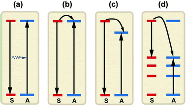 | ||
| Fig. 6 A schematic diagram to illuminate the different ET processes between two ions: (a) resonant radiative transfer through emission of a sensitizer and re-absorption by an activator; (b) nonradiative transfer associated with resonance between a sensitizer and an activator; (c) multiphonon assisted ET; and (d) cross-relaxation between two identical ions. S and A denote the sensitizer and activator, respectively. | ||
The Dexter ET probability from a sensitizer (S) to an activator (A) is generally approximated as in eqn (5):69
 | (5) |
Phonon-assisted ET occurs when the resonance condition is not well met between the sensitizer and the activator, resulting in a small spectral overlap (Fig. 6c). In this case, the mismatch between the transition energies of the sensitizer and the activator is compensated by phonon emission or absorption. According to Miyakawa–Dexter theory,70 the probability of phonon-assisted transfer is expressed by,
| PPAT(ΔE) = PPAT(0)e−βΔE | (6) |
Cross-relaxation terminology usually refers to all types of resonant ET between identical ions, acting as both sensitizers and activators. As shown in Fig. 6d, cross-relaxation may give rise to the diffusion process between sensitizers when the levels involved are identical (known as energy migration) or to self-quenching when their levels are different. In the first case there is no loss of energy, whereas in the second there is a loss or change in the energy of the emitted photons.68 Concentration quenching of luminescence often takes place as a result of cross-relaxation among the activators when the concentration of the activator is above a critical value.
3. Upconversion materials for PV applications
3.1 Concepts of upconversion
The term upconversion describes nonlinear anti-Stokes optical processes that convert two (or more) low-energy pump photons to a higher-energy output photon.72,73 This phenomenon was first discovered by Auzel in the 1960s.74 Since then, there has been a surge of research interest in upconversion due to its applications in a number of diverse fields, such as infrared quantum counter detectors, compact solid-state lasers, temperature sensors, lightings and displays, as well as biomedical imaging.75–137As was already discussed above, only the absorption of photons with energy higher than the bandgap can generate electron–hole pairs contributing to electric current. Indeed, the transmission of sub-bandgap photons is one of the major energy loss mechanisms in conventional solar cells. In the case of c-Si solar cells, the transmission loss amounts to about 20% of the incident solar energy, which is not substantially reducible by conventional approaches. To this end, the use of upconversion materials may provide a solution to the transmission loss by converting two sub-bandgap photons into one above-bandgap photon. Indeed, Trupke et al.32 in 2002 showed that the theoretical efficiency limit of a solar cell, modified with an up-converter, can reach 63.2% for concentrated sunlight and 47.6% for non-concentrated sunlight, respectively.
Although the idea of using upconversion for improving the performance of solar cell devices is implicit, relatively little work has been done until recently. A considerable limitation lies in the fact that upconversion processes are only possible in trivalent lanthanide ions with metastable and long-lived intermediate levels acting as storage reservoirs for the pump energy. In this sense, Er3+, Tm3+, and Ho3+ ions, featuring ladder-like energy levels for facilitating photon absorption and subsequent ET steps, were generally chosen as activators to give rise to efficient visible emissions under low pump power densities. In order to enhance upconversion luminescence efficiency, the Yb3+ ion is usually co-doped as an excellent upconversion sensitizer due to its large absorption cross-section in the 900–1100 nm NIR region, corresponding to the 2F5/2 → 2F7/2 (Yb3+) transition. In fact, the Er3+–Yb3+ couple is by far the most studied upconversion system (Fig. 7).
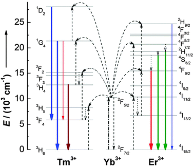 | ||
| Fig. 7 Proposed upconversion mechanisms for Er3+–Yb3+ and Tm3+–Yb3+ couples under 980 nm diode laser excitation. The dash-dotted, dashed, dotted, and full arrows represent photon excitation, energy transfer, multiphonon relaxation, and emission processes, respectively. Only visible and NIR emissions are shown here. (Reprinted with permission from ref. 77. Copyright 2008, American Chemical Society.) | ||
A wide variety of upconversion mechanisms have been identified (Fig. 8). For PV applications, the majority of these mechanisms are based on some combination of excited state absorption (ESA) and energy transfer upconversion (ETU) processes. In contrast to common nonlinear processes including two photon absorption and second harmonic generation, these upconversion processes combine the benefit of high quantum efficiency without the need for intense coherent excitation sources, with the inherent advantages of large anti-Stokes shift. ESA is a single-ion process that involves sequential absorption of two (or more) photons by an excited ion using a real intermediary energy level, and results in promotion of that ion to a higher excited state. In ETU, two pump photons excite two neighboring ions to a metastable energy level through ground-state absorption (GSA). The excited ions then exchange energy nonradiatively, promoting one excited ion to an upper emitting state and demoting the other ion to the ground state. Photon avalanche (PA) is an unconventional mechanism as it could lead to strong upconverted emission without any resonant GSA when the pump power is above a certain threshold value.138 The pump wavelength is only resonant between a metastable state and a higher energy level. The phenomenon of PA upconversion was first reported in Pr3+-doped LaCl3 and LaBr3 crystals.139 Recently, Wang et al.75 proposed the energy migration-mediated upconversion (EMU) involving the use of four types of lanthanide ions and a core–shell structure. Through gadolinium sublattice-mediated energy migration, efficient tunable upconversion emissions in NaGdF4:Tm3+/Yb3+@NaGdF4:Ln3+ core–shell nanoparticles were realized for various lanthanide activators (Ln3+ = Eu3+, Tb3+, Dy3+, and Sm3+) without long-lived intermediary energy states.
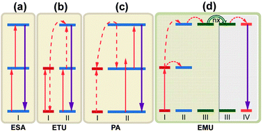 | ||
| Fig. 8 Proposed typical upconversion processes. (a) Excited state absorption (ESA); (b) energy transfer upconversion (ETU); (c) photon avalanche (PA). PA is an unconventional mechanism as it could lead to strong upconverted emission without any resonant ground-state absorption when the pump power is above a certain threshold value. The pump wavelength is only resonant between a metastable state and a higher energy level; (d) energy migration-mediated upconversion (EMU) involving the use of four types of lanthanide ions and a core–shell design. Note that core and shell regions are highlighted with different background colors. The ‘nx’ denotes the occurrence of random hopping through many type-III ions. | ||
The use of upconversion materials for improving PV system performance was first reported by Gibart's group140 in 1996 using the Er3+–Yb3+ couple in bifacial GaAs solar cells. Since then, many groups have pursued the development of various upconversion-based PV devices to enhance the conversion efficiency (Table 2).141–164 Upconversion materials singly-doped with Er3+ or Ho3+, capable of converting long-wavelength NIR light into short-wavelength NIR and visible emissions, can be combined with narrow bandgap c-Si solar cells (Eg = 1.12 eV; 1100 nm). For PV devices using wide bandgap semiconductors, such as GaAs (Eg = 1.43 eV; 867 nm)165 and amorphous Si (Eg = 1.75 eV; 708 nm),166 the utilization of upconversion materials co-doped with Ln3+–Yb3+ couples is very convenient due to the efficient ETU from the Yb3+ sensitizer to various Ln3+ activators.
| Dopant ion | Host lattice | Preparation method | Excitation (nm) | Emission (nm) | Solar cell type | Ref. |
|---|---|---|---|---|---|---|
| Er3+ | NaYF4 | Solid-state reaction | 1523 | 550, 660, 800, 980 | c-Si | 141 |
| Er3+ | NaYF4 | — | 1523 | 545, 670, 800, 980 | c-Si | 142 |
| Er3+ | CaF2 | — | 1550 | 660, 980 | c-Si | 143 |
| Er3+ | Gd2(MoO4)3 | Combustion synthesis | 1530 | 545, 665, 800, 980 | c-Si | 144 |
| Er3+ | Y2O3 | Template technology | 1538 | 562, 659, 801, 987 | c-Si | 145 |
| Er3+ | Fluoride glasses | Glass melting | 1532 | 550, 660, 820, 980 | c-Si | 146 |
| Ho3+ | Glass ceramics containing PbF2 nanocrystals | Glass melting | 1170 | 650, 910 | c-Si | 147 |
| Ho3+–Yb3+ | Fluoroindate glass | Glass melting | 1155 | 550, 650, 750, 905, 980 | c-Si | 148 |
| Er3+–Yb3+ | Y6W2O15 | Solid-state reaction | 973 | 516–570 | GaAs | 149 |
| Er3+–Yb3+ | NaYF4 | Hydrothermal method | 980 | 525, 540, 655 | Amorphous Si | 150,151 |
| Er3+–Yb3+ | NaYF4 | Solid-state reaction | 980 | 522, 540, 653 | Amorphous Si | 152 |
| Er3+–Yb3+ | NaYF4 | Hydrothermal method | 980 | 524, 540, 660 | Amorphous Si | 153 |
| Er3+–Yb3+ | Glass ceramic containing NaYF4 nanocrystals | Glass melting | 980 | 520, 538, 656 | Amorphous Si | 154 |
| Er3+ | Y2O3 | Hydrothermal method | 980 | 525, 550, 660 | Dye-sensitized | 155 |
| Er3+–Yb3+ | LaF3 | Solvothermal synthesis | 980 | 543, 655 | Dye-sensitized | 156 |
| Er3+–Yb3+ | NaYF4 | Hydrothermal method | 980 | 510–570, 640–680 | Dye-sensitized | 157 |
| Er3+–Yb3+ | NaYF4:Er,Yb@NaYF4 |
Thermal decomposition | 976 | 510–570, 635–700 | Dye-sensitized | 158 |
| Er3+–Yb3+ | YF3 | Thermal decomposition | 980 | 525, 545, 656 | Dye-sensitized | 159 |
| Er3+–Yb3+ | YAG transparent ceramics | Solid-state reaction | 980 | 520, 563, 677 | Dye-sensitized | 160 |
| Tm3+–Yb3+ | Lu2O3 | Co-precipitation | 980 | 476, 653 | Dye-sensitized | 161 |
| Tm3+–Yb3+ | Glass ceramics containing PbF2 nanocrystals | Glass melting | 980 | 475, 650, 800 | Dye-sensitized | 162 |
| Er3+–Yb3+ | YF3 | — | 975 | 510–560 | Organic | 163 |
| Ho3+–Yb3+ | Y2BaZnO5 | Solid-state reaction | 986 | 545 | Organic | 164 |
3.2 Upconversion for c-Si solar cells
 | ||
| Fig. 9 Upconversion processes via the ETU mechanism between two Er3+ ions, resulting in c-Si above-bandgap emissions under c-Si sub-bandgap pump excitation (1520 nm). Solid, dotted, and wavy arrows represent photon absorption/emission, energy transfer, and multiphonon relaxation, respectively. | ||
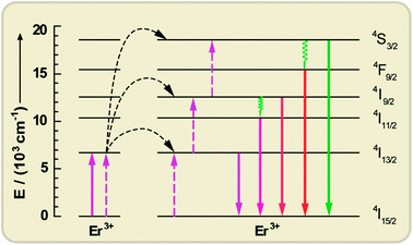
Shalav et al.141 in 2005 reported the application of NaYF4:Er3+ (20 mol%) phosphors as the upconverters in a bifacial c-Si solar cell. These phosphors were mixed into an optically transparent acrylic adhesive medium at a concentration of 40 wt% and then placed on the rear of a bifacial c-Si solar cell. Reflective white paint was used as a reflector on the rear of the system. An external quantum efficiency of 2.5% was obtained for the solar cell under excitation at 1523 nm with a 5.1 mW laser. More recently, Fischer and co-workers142 also investigated the potential of NaYF4:Er3+ to significantly reduce the sub-bandgap losses of c-Si solar cells. The optical upconversion efficiency of NaYF4:Er3+ (20 mol%) was determined to be about 5.1% upon excitation at 1523 nm with a power density of 1880 W m−2. The c-Si solar cell device combined with an upconverter showed an external quantum efficiency of 0.34% upon irradiation at 1522 nm with a power density of 1090 W m−2.
In a following paper, Lahoz et al.148 co-doped Ho3+ with Yb3+ and found enhanced emission intensity of NIR-to-NIR upconversion as a result of ET from Ho3+ to Yb3+ ions. Importantly, owing to the high transparency to the excitation wavelength of ∼1540 nm, these Ho3+-based glass ceramics could be used in combination with Er3+-doped upconverters. The authors proposed a double-layer design with the Ho3+-doped upconverting layer placed directly at the rear surface of a bifacial c-Si solar cell, followed by the Er3+-doped upconverter and a mirror (Fig. 10). The integration of both upconverters would enlarge the absorption of the solar sub-bandgap spectral range exploited for enhancing the c-Si solar cell response.
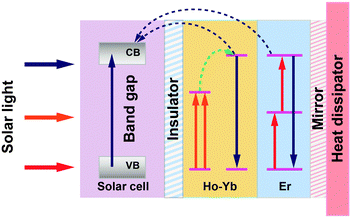 | ||
| Fig. 10 A proposed operating mechanism for a c-Si solar cell with Ho3+–Yb3+ and Er3+ doped upconverters. Above-bandgap light (highlighted in blue color) is directly absorbed by the solar cell, which is electronically isolated from the upconverter. The sub-bandgap light (highlighted in orange and red colors) transmitted by the solar cell is stepwise upconverted into high-energy photons, which are subsequently absorbed in the solar cell. A mirror reflector is located behind the upconverter. CB and VB are the conduction and valence bands of c-Si, respectively. The energy gap between VB and CB is around 1.12 eV for c-Si. | ||
An alternative design proposed by Chen et al. in 2012 is to adopt a core–shell nanostructure, in which Er3+ and Ho3+ activators are separately incorporated into the core and shell layer of a nanoparticle.167 The use of a core–shell layout can extend the NIR wavelength range excitable for upconversion emission, and furthermore allow facile modulation of activator concentration while minimizing luminescence quenching induced by the deleterious cross-relaxation ET between the Er3+ and Ho3+ ions. As a proof-of-concept experiment, the authors fabricated monodisperse NaGdF4:Er3+@NaGdF4:Ho3+@NaGdF4 core–shell–shell nanoparticles. The middle protection shell not only enhances the upconversion luminescence of Er3+ in the core, but also acts as the host to realize the upconversion luminescence of Ho3+. As a result, intense upconversion emissions for both Er3+ and Ho3+ dopants were achieved.
3.3 Upconversion for wide bandgap solar cells
The same upconversion phosphor was also used by de Wild et al.151,152 to demonstrate enhanced conversion efficiency in amorphous Si solar cells. In their experiments, the upconversion powders were mixed with polymethylmethacrylate and then made into an upconverter layer with thickness of 200–300 μm. A maximum current enhancement of 6.2 mA was measured under 980 nm diode laser illumination at 28 mW. More recently, a 72-fold enhancement in photocurrent under 980 nm illumination was achieved by Li et al.153 using NaYF4:Yb3+/Er3+/Gd3+ nanorod-modified electrodes in an amorphous Si solar cell, as compared to the PV cell without an upconverter.
In a following paper by Shan et al.,157 different upconversion materials consisting of NaYF4:Er3+/Yb3+ hexagonal nanoplatelets (particle size ∼800 nm) were tested in DSSCs. The upconverting phosphors were directly placed on the rear side of a counter electrode (Fig. 11). This design enables a dual-mode functionality that provides both light reflection and NIR light harvesting. Photocurrent was observed for the DSSC device when illuminated with a 980 nm fiber laser, clearly demonstrating the upconverting function of the NaYF4:Er3+/Yb3+ nanomaterials. Importantly, this novel DSSC configuration greatly overcomes the drawback of charge recombination induced by the conducting upconversion layer when used internally. Moreover, the authors found that under AM 1.5G filtered spectral illumination (100 mW cm−2) approximately 10% enhancement in both photocurrent and overall conversion efficiency can be achieved by addition of the upconverting layer, which was predominantly attributable to its light reflecting role. Several other groups also reported the enhanced NIR response of the DSSCs by using upconverting materials doped with Er3+,155 Er3+–Yb3+,158–160 and Tm3+–Yb3+.161
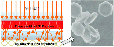 | ||
| Fig. 11 Schematic configuration of a DSSC device consisting of one internal TiO2 transparent layer and an external rear layer of NaYF4:Er3+/Yb3+ hexagonal nanoplatelets. The external upconverting layer can simultaneously reflect scattered light and harvest NIR light. (Reprinted with permission from ref. 157. Copyright 2011, American Chemical Society.) | ||
In 2012, Adikaari et al. applied Y2BaZnO5:Ho3+/Yb3+ upconversion phosphors to PCDTBT:PCBM (PCDTBT: poly[N-9′-hepta-decanyl-2,7-carbazole-alt-5,5(4′,7′-di-2-thienyl-2′,1′,3′-benzothiadiazole]) organic solar cells in order to utilize the NIR solar spectrum.164 The authors adopted two different layout designs for the PV device as shown in Fig. 12a and b. The PCDTBT:PCBM active layer showed little absorption for light with wavelengths above 700 nm, while the Y2BaZnO5:Er3+/Yb3+ phosphors exhibited a broad absorption band in the region of 870–1030 nm due to the 2F7/2 → 2F5/2 (Yb3+) transition (Fig. 12c). Moreover, the main upconversion emission at 545 nm that corresponds to 5S2,5F4 → 5I8 (Ho3+) transition matches well with the absorption of the PCDTBT:PCBM photoactive layer (Fig. 12d). Their PV measurements showed that with the upconversion phosphors placed behind the device, a maximum photocurrent density of 16 μA cm−2 and a power conversion efficiency of 0.45% were obtained when illuminated with a 986 nm laser (excitation density: ∼390 mW cm−2).
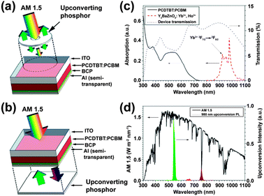 | ||
| Fig. 12 Schematic design of an organic PV device with upconversion phosphors placed (a) in front of or (b) behind the device. (c) Absorption spectra of PCDTBT:PCBM and Ho3+–Yb3+ co-doped Y2BaZnO5 phosphors and the corresponding transmission spectrum of the PV device. (d) AM1.5G spectrum and upconversion emission spectrum of Ho3+–Yb3+ co-doped Y2BaZnO5 phosphors under 986 nm excitation. Note that the separation distance between the phosphor layer and the device is ∼0.5 mm. ITO and BCP refer to indium tin oxide and bathocuproine, respectively. (Reprinted with permission from ref. 164. Copyright 2012, American Institute of Physics.) | ||
Before the conversion efficiency of PV devices can be further improved through use of upconversion materials, though, it will be necessary to put some effort into addressing a number of challenges. First, only a small fraction of the solar spectrum can be upconverted by Ln3+-doped materials because of their weak and narrowband absorption, so the next step will be to explore methods that enable broadband upconversion. More significantly, new materials or technologies enabling high upconversion efficiency must be developed as upconversion is a nonlinear process with low conversion efficiency (typically less than 3%).194 A high-density excitation, controlled by a pulsed laser, can enhance upconversion efficiency. But for practical PV applications, the need for concentrated solar power clearly complicates the manufacture of solar cells. In this regard, photon upconversion based on sensitized triplet–triplet annihilation (TTA) involving chromophores could be utilized for wide bandgap solar cells. This emerging technology offers relatively high upconversion efficiency under low excitation power density (a few mW cm−2).195–198 Sunlight is sufficient to excite the chromospheres and sensitize the upconversion process. However, a significant drawback of TTA is that the upconverted spectrum is generally limited in the range of 650–700 nm.199 Although several groups have recently reported the TTA-based NIR-to-visible upconversion, thus far the attempts to obtain efficient upconverted emissions at wavelengths beyond 800 nm have not been successful.200–202
4. Quantum-cutting materials for PV applications
4.1 Concepts of quantum-cutting
There are certain phosphor materials that can transform the energy of one absorbed photon into two (or more) emitted low-energy photons. This process is known as quantum-cutting with quantum efficiency more than 100%.33 In general, quantum-cutting can be realized by photon cascade emission from a single lanthanide ion (e.g. Pr3+64–66 and Gd3+203) or by downconversion via ET through different sets of lanthanide ions (e.g. Gd3+–Eu3+62,63 and Gd3+–Tb3+–Er3+).204 The first successful demonstration of efficient visible quantum-cutting in a LiGdF4:Eu3+ phosphor was reported by Wegh et al. in 1999 with a theoretical quantum efficiency of 190%.62,63 The search for new quantum-cutting materials has gained importance in recent times in view of their promising applications in plasma display panels and mercury-free fluorescent tubes.33,205–221Recently, the potential of using quantum-cutting phosphors in c-Si solar cells has been explored in an effort to maximize their efficiency.222 Trupke et al. have performed theoretical calculations that predict an enhancement up to 38.6% in conversion efficiency for a solar cell modified with a quantum-cutting layer.34 The NIR quantum-cutting has been demonstrated in various Ln3+–Yb3+ (Ln = Tb, Tm, Pr, Er, Nd, Ho, and Dy) co-doped systems (Table 3)223–237 and in phosphors with a single luminescent center (Ho3+, Tm3+, or Er3+).238–243
| Dopant ion | Host lattice | Preparation method | Excitation (nm) | ET type | Maximum quantum efficiency (%) | Ref. |
|---|---|---|---|---|---|---|
| Tb3+–Yb3+ | YPO4 | Solid-state reaction | 489 | Second-order cooperative | 188 | 223 |
| Tb3+–Yb3+ | GdBO3 | Combustion synthesis | 486 | Second-order cooperative | 182 | 224 |
| Tb3+–Yb3+ | Zn2SiO4 thin-films | Sol–gel method | 485 | Second-order cooperative | 162 | 225 |
| Tm3+–Yb3+ | GdAl3(BO3)4 | Combustion synthesis | 475 | Second-order cooperative | 164 | 226 |
| Tm3+–Yb3+ | Glass ceramics containing LaF3 nanocrystals | Glass melting | 468 | Second-order cooperative | 162 | 227 |
| Tm3+–Yb3+ | YPO4 | Co-precipitation | 468 | First-order phonon-assisted | 175 | 228 |
| Pr3+–Yb3+ | GdAl3(BO3)4 | Combustion synthesis | 489 | Second-order cooperative | 165 | 226 |
| Pr3+–Yb3+ | NaYF4 | Hydrothermal method | 443 | Second-order cooperative | 181 | 229 |
| Pr3+–Yb3+ | SrF2 | Solid-state reaction | 441 | First-order resonant | 140 | 230 |
| Er3+–Yb3+ | NaYF4 | Solid-state reaction | 380 | First-order resonant | 128 | 231 |
| Er3+–Yb3+ | Cs3Y2Br9 | Vertical Bridgman | 490 | First-order resonant | 195 | 232 |
| Nd3+–Yb3+ | YF3 | Co-precipitation | 360 | First-order resonant | 140 | 233 |
| Ho3+–Yb3+ | Glass ceramics containing YF3 nanocrystals | Glass melting | 488 | First-order resonant | 159 | 234 |
| Ho3+–Yb3+ | NaYF4 | Hydrothermal method | 535 | First-order resonant | 182 | 235 |
| Ho3+–Yb3+ | NaYF4 | Hydrothermal method | 359 | First-order resonant | 155 | 236 |
| Dy3+–Yb3+ | Zeolites | Ion-exchange process | 430 | First-order resonant | – | 237 |
Several mechanisms responsible for the NIR quantum-cutting are illustrated in Fig. 13. The first mechanism is based on one luminescent center with three energy levels (Fig. 13a). It is possible to sequentially produce two NIR photons after transition of the optical center to the highest energy level by absorption of one ultraviolet or visible photon. The intermediate level is shortly populated before the optical center returns to its ground state. Representative examples have been reported for single ions like Ho3+, Tm3+, or Er3+.238–243 However, one major problem presented by single ion-based quantum-cutting is the unwanted emissions in the ultraviolet–visible spectral range and nonradiative recombination that compete with the desired emission of two NIR photons.
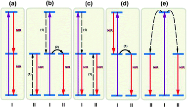 | ||
| Fig. 13 Summary of typical mechanisms of NIR quantum-cutting for PV applications. Simplified energy level diagrams for ions (types I and II) are given to illustrate the concept of NIR quantum-cutting. (a) NIR quantum-cutting on a single ion by the sequential emission of two NIR photons. (b–d) NIR quantum-cutting due to resonant ET from ion I to ion II. (e) NIR quantum-cutting due to cooperative ET from ion I to ion II. Note that two type II ions simultaneously emit two photons in the NIR spectral region. The purple solid, red solid, and dashed arrows represent excitation, emission, and ET processes (cross-relaxation for b,c and cooperative ET for e), respectively. | ||
Alternative mechanisms involving two luminescent centers for NIR quantum-cutting are summarized in Fig. 13b–e. A plausible mechanism occurs via a two-step ET process through ion pairs of physically interacting lanthanide ions, accompanied by the emission of two NIR photons (Fig. 13b). This quantum-cutting mechanism has been reported in Pr3+–Yb3+,230 Er3+–Yb3+,232 Nd3+–Yb3+,233 Ho3+–Yb3+,236 and Dy3+–Yb3+ co-doped systems.237 The emission of two NIR photons can also be achieved by quantum-cutting involving one-step ET between two optical centers (Fig. 13c and d). The quantum-cutting mechanism illustrated in Fig. 13c has been experimentally validated for phosphors doped with Tm3+–Yb3+,228 Er3+–Yb3+,231 and Ho3+–Yb3+ couples.234,235 To the authors' knowledge, there is no experimental investigation reported on the mechanism shown in Fig. 13d.
The quantum-cutting mechanisms discussed in Fig. 13b–d require resonance ET between two optical centers in close proximity. The ET can be described as a first-order rate process, governed by the degree of overlap between the donor emission and the acceptor absorption. Energy splitting is plausible by population of an intermediate energy level of the donor. In contrast, if there is no spectral overlap, a second-order cooperative sensitization may dominate the relaxation process, resulting in simultaneous excitation of two acceptors and subsequent emission of two NIR photons (Fig. 13e). For efficient cooperative sensitization to be observed, the sum of the energy of the absorption transitions of the two acceptors must equal the energy of the donor emission.223 This cooperative quantum-cutting has been extensively investigated in Tb3+–Yb3+,223–225 Tm3+–Yb3+,226,227 and Pr3+–Yb3+ co-doped systems.226,229 While the performance enhancement achieved was encouraging, it should be noted that the possibility of the second-order cooperative ET process is about 1000 times lower than that of the first-order resonant ET process.230 Thus, a high doping content of Yb3+ is typically required for realizing efficient cooperative quantum-cutting.
4.2 Narrowband quantum-cutting for c-Si solar cells
000 cm−1) is approximately twice the energy of the 2F7/2 → 2F5/2 transition of Yb3+ (∼10000 cm−1).
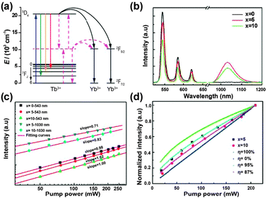 | ||
| Fig. 14 (a) Schematic partial energy-level diagram of the Tb3+–Yb3+ couple, showing the ET mechanism of NIR quantum-cutting under the excitation of the 7F6 → 5D4 (Tb3+) transition. Black solid lines show the second-order nonlinear quantum-cutting process, whereas the red dotted lines show the linear downconversion process where a virtual energy level located at the middle position (around 10000 cm−1) between the ground state and the 5D4 energy level of Tb3+ participates in the quantum-cutting process. (b) Emission spectra of NaYF4:Tb3+/Yb3+ (1/x mol%, x = 0, 5, and 10) phosphors under 473 nm laser excitation. (c) Double logarithmic plot of Tb3+ and Yb3+ emission intensity versus pump power of the 473 nm laser for NaYF4:Tb3+/Yb3+ (1/x mol%, x = 0, 5, and 10) phosphors. (d) Experimental and simulated power dependence curves of Yb3+ luminescence for NaYF4:Tb3+/Yb3+ (1/x mol%, x = 0, 5, and 10) phosphors. (Reprinted with permission from ref. 249. Copyright 2012, Optical Society of America.) | ||
The ET process from Tb3+ to Yb3+ was investigated by the steady-state and time-resolved luminescence spectroscopy. The ET and quantum efficiencies were calculated from the luminescence decay curves using the following equations,
 | (7) |
| ηQE = ηTb(1 − ηET) + 2ηET | (8) |
Although various Tb3+–Yb3+ co-doped materials have been well studied, the issue of the underlying ET mechanism from Tb3+ to Yb3+ ions is still debatable.244–249 Some researchers believed that a nonlinear second-order downconversion process should be responsible for the cooperative quantum-cutting (Fig. 14a).244,245 The slope of Yb3+ luminescence intensity versus the excitation power was found to be nearly 0.5, indicating the emission of two lower-energy photons upon the absorption of one photon. On the other hand, two different groups found the slope of luminescence intensity curves to be near 1 instead of 0.5, indicating a one-photon process for the Yb3+ NIR emission.246,247 A similar result was also obtained by Duan and co-workers in Tb3+–Yb3+ co-doped oxyfluoride glass,248 but they attributed it to a linear cooperative quantum-cutting mechanism. In this case, a virtual energy level of Tb3+ located around 10000 cm−1 could participate in the quantum-cutting process (Fig. 14a), and the downconversion emission intensity would increase linearly with the excitation intensity (Fig. 14b). Interestingly, it was experimentally found that in NaYF4 host materials the slopes of Yb3+ luminescence power dependence curves were fitted to be between 0.5 and 1 (Fig. 14c and d).249 This sublinear power dependence phenomenon was attributed to the combination of a linear downconversion process and a dominant second-order nonlinear process.
000 cm−1 or 475 nm). The energy of the 1G4 → 3H6 transition of Tm3+ is about twice as large as the 2F5/2 → 2F7/2 transition of Yb3+. Thus, the excited 1G4 (Tm) state can simultaneously transfer its energy to two neighboring Yb3+ ions, subsequently resulting in NIR emission in the range of 950–1100 nm (Fig. 15a). Notably, no convincing evidence thus far for the cooperative ET mechanism has been reported. As a result, it is still controversial whether the second-order cooperative or first-order ET dominates the visible-to-NIR quantum-cutting process.
![Schematic partial energy-level diagrams of Tm3+ and Yb3+ ions, showing the quantum-cutting mechanisms for the Tm3+–Yb3+ couple upon blue excitation of Tm3+ to the 1G4 state. (a) Quantum-cutting via second-order cooperative ET. The excited energy is simultaneously transferred to two Yb3+ ions, resulting in two NIR photons of Yb3+ ions around 1000 nm. (b) Quantum-cutting via first-order phonon-assisted ET. Part of the excited energy is transferred to one Yb3+ ion through the phonon-assisted ET process [Tm3+ (1G4 → 3H5); Yb3+ (2F7/2 → 2F5/2)], which populates the 3H5 (Tm3+) state and leads to another mid-IR emission from the 3F4 (Tm3+) state at around 1800 nm through fast nonradiative relaxation from 3H5. Note that the energy gap between 3H5 and 3F4 states is about 2250 cm−1. Dotted and solid arrows represent nonradiative ET pathways and optical transitions, respectively. (Reprinted with permission from ref. 228. Copyright 2012, Owner Societies.)](/image/article/2013/CS/c2cs35288e/c2cs35288e-f15.gif) | ||
| Fig. 15 Schematic partial energy-level diagrams of Tm3+ and Yb3+ ions, showing the quantum-cutting mechanisms for the Tm3+–Yb3+ couple upon blue excitation of Tm3+ to the 1G4 state. (a) Quantum-cutting via second-order cooperative ET. The excited energy is simultaneously transferred to two Yb3+ ions, resulting in two NIR photons of Yb3+ ions around 1000 nm. (b) Quantum-cutting via first-order phonon-assisted ET. Part of the excited energy is transferred to one Yb3+ ion through the phonon-assisted ET process [Tm3+ (1G4 → 3H5); Yb3+ (2F7/2 → 2F5/2)], which populates the 3H5 (Tm3+) state and leads to another mid-IR emission from the 3F4 (Tm3+) state at around 1800 nm through fast nonradiative relaxation from 3H5. Note that the energy gap between 3H5 and 3F4 states is about 2250 cm−1. Dotted and solid arrows represent nonradiative ET pathways and optical transitions, respectively. (Reprinted with permission from ref. 228. Copyright 2012, Owner Societies.) | ||
Most recently, Zheng et al.228 in 2012 showed that in YPO4:Yb3+/Tm3+ phosphors the visible-to-NIR quantum-cutting can be induced by the first-order phonon-assisted ET. In their study, one incident blue photon is cut into one NIR photon of Yb3+ (2F5/2 → 2F7/2, ∼1000 nm) and one mid-IR photon of Tm3+ (3F4 → 3H6, ∼1800 nm), rather than two NIR photons from Yb3+ (Fig. 15b). Pump power dependence studies on Yb3+ emission intensity revealed that only one emitting photon of Yb3+ can be achieved per absorbed blue photon. Importantly, such phonon-assisted quantum-cutting luminescence for the Tm3+–Yb3+ couple can only be realized in those host materials with high phonon energies (such as phosphates, borates, and silicates) because of the large energy mismatch (∼2500 cm−1) between 1G4 → 3H5 (Tm3+) and 2F7/2 → 2F5/2 (Yb3+) transitions. Although YPO4 host material with the maximum phonon energy of about 1070 cm−1 meets this requirement, the material is not suitable for c-Si PV application as the mid-IR photon is beyond the absorption edge of the c-Si.
Jaffres et al.257 in 2012 investigated the optical property of Tm3+–Yb3+ co-doped La2BaZnO5 phosphors with a maximum phonon energy of ∼600 cm−1. Upon excitation of Tm3+ to the 1G4 level, they found no noticeable ET from Tm3+ to Yb3+, only cascade emission of three mid-IR photons due to 3F4 → 3H6 transition of Tm3+. This result is attributed to two successive cross-relaxation steps between Tm3+ ions.
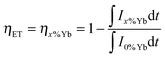
700 cm−1) is about twice the energy of the 2F5/2 → 2F7/2 transition of Yb3+;226,229,258–261 or (ii) first-order resonant ET via two sequential steps involving cross-relaxation [Pr3+ (3P0 → 1G4); Yb3+ (2F7/2 → 2F5/2)] followed by a second ET process [Pr3+ (1G4 → 3H4); Yb3+ (2F7/2 → 2F5/2)] (Fig. 16a).230,262–273
 | ||
| Fig. 16 (a) NIR quantum-cutting via the first-order ET mechanism for the Pr3+–Yb3+ couple. A two-step ET occurs upon excitation onto the 3PJ (J = 0, 1, 2) and 1I6 levels of Pr3+, using the 1G4 level as an intermediate state. A single blue photon absorbed by these levels is converted into two NIR photons of ∼1000 nm. (b) Emission spectra for SrF2:Pr3+/Yb3+ (0.1/x mol%; x = 0, 5, and 17) under excitation at 441 nm. (c) Diffuse reflectance (dashed line) and excitation spectra (solid line) of the SrF2:Pr/Yb (0.1/5 mol%) sample. (d) Luminescence decay curves of the 3P0 → 3H4 emission at 486 nm in SrF2:Pr/Yb (0.1/x mol%; x = 0, 0.2, 1, 5, and 17) under excitation at 441 nm. (Reprinted with permission from ref. 230. Copyright 2009, Wiley-VCH Verlag GmbH & Co. KGaA.) | ||
Meijerink and co-workers263 argued that the dominant quantum-cutting mechanism in the Pr3+–Yb3+ couple appears to be first-order ET by cross relaxation, because the reduced cross-relaxation rate can be compensated by the much higher (∼1000 times) probability of first-order ET relative to the second-order cooperative ET process. This first-order ET scheme leads to efficient quantum-cutting of one 441 nm blue photon into two 980 nm NIR photons in SrF2:Pr3+,Yb3+ phosphors.230 Comparison of emission spectra for SrF2:Pr3+ (0.1 mol%) and SrF2:Pr3+,Yb3+ (0.1/5%) samples (Fig. 16b) revealed an actual conversion efficiency of 140%. Furthermore, the 980 nm photon flux upon excitation of Pr3+ to the 3PJ,1I6 (J = 0, 1, and 2) levels is approximately twice that of the absorption strength of the 3PJ,1I6 levels (Fig. 16c), confirming that for every photon absorbed to the 3PJ,1I6 levels, two photons in the NIR were generated. Introduction of Yb3+ into SrF2:Pr3+ induced faster and nonexponential decay of 3P0 → 3H4 emission (Fig. 16d), thus providing additional evidence for the ET from Pr3+ to nearby Yb3+ ions.
000 cm−1 (4F7/2) and 10000 cm−1 (4I11/2) that allow for a two-step ET process, raising two neighboring Yb3+ ions to the 2F5/2 excited state around 10000 cm−1. Upon 490 nm excitation at the 4F7/2 level, the cross-relaxation process of [Er3+ (4F7/2 → 4I11/2); Yb3+ (2F7/2 → 2F5/2)] can occur, followed by a second ET step of [Er3+ (4I11/2 → 4I15/2); Yb3+ (2F7/2 → 2F5/2)]. Both Yb3+ ions then emit a NIR photon of ∼1000 nm that can be absorbed by a c-Si solar cell (Fig. 17a).
![(a) Schematic partial energy-level diagrams for the Er3+–Yb3+ couple showing the quantum-cutting mechanism starting from the 4F7/2 level. A single blue photon absorbed by Er3+ is converted into two ∼1000 nm NIR photons of Yb3+via two sequential ET steps: (1) cross-relaxation ET of [Er3+ (4F7/2 → 4I11/2); Yb3+ (2F7/2 → 2F5/2)]; (2) cross-relaxation ET of [Er3+ (4I11/2 → 4I15/2); Yb3+ (2F7/2 → 2F5/2)]. (b) Schematic partial energy-level diagrams for the Nd3+–Yb3+ couple showing the quantum-cutting mechanism starting from the 2G9/2 level. A single blue photon absorbed by Nd3+ is downconverted into two ∼1000 nm NIR photons of Yb3+ ions via two-step ET mechanisms: (1) cross-relaxation ET of [Nd3+ (2G9/2 → 4F3/2); Yb3+ (2F7/2 → 2F5/2)]; (2) cross-relaxation ET of [Nd3+ (4F3/2 → 4I9/2); Yb3+ (2F7/2 → 2F5/2)]. (c) Schematic partial energy-level diagrams for the Er3+–Yb3+ couple showing the quantum-cutting mechanism starting from the 4F9/2 level. One blue photon absorbed by Dy3+ is downconverted into two NIR photons from Yb3+ through two sequential ET steps: (1) cross-relaxation ET of [Dy3+ (4F9/2 → 6H5/2); Yb3+ (2F7/2 → 2F5/2)]; (2) cross-relaxation ET of [Dy3+ (6H5/2 → 6H15/2); Yb3+ (2F7/2 → 2F5/2)]. (d) Schematic partial energy-level diagrams for the Ho3+–Yb3+ couple showing the quantum-cutting mechanism starting from the 5S2,5F4 level. Note that the 5F3 level of Ho3+ is located at ∼20 600 cm−1, while the 5S2,5F4 level is located at ∼18 600 cm−1.](/image/article/2013/CS/c2cs35288e/c2cs35288e-f17.gif) | ||
| Fig. 17 (a) Schematic partial energy-level diagrams for the Er3+–Yb3+ couple showing the quantum-cutting mechanism starting from the 4F7/2 level. A single blue photon absorbed by Er3+ is converted into two ∼1000 nm NIR photons of Yb3+via two sequential ET steps: (1) cross-relaxation ET of [Er3+ (4F7/2 → 4I11/2); Yb3+ (2F7/2 → 2F5/2)]; (2) cross-relaxation ET of [Er3+ (4I11/2 → 4I15/2); Yb3+ (2F7/2 → 2F5/2)]. (b) Schematic partial energy-level diagrams for the Nd3+–Yb3+ couple showing the quantum-cutting mechanism starting from the 2G9/2 level. A single blue photon absorbed by Nd3+ is downconverted into two ∼1000 nm NIR photons of Yb3+ ions via two-step ET mechanisms: (1) cross-relaxation ET of [Nd3+ (2G9/2 → 4F3/2); Yb3+ (2F7/2 → 2F5/2)]; (2) cross-relaxation ET of [Nd3+ (4F3/2 → 4I9/2); Yb3+ (2F7/2 → 2F5/2)]. (c) Schematic partial energy-level diagrams for the Er3+–Yb3+ couple showing the quantum-cutting mechanism starting from the 4F9/2 level. One blue photon absorbed by Dy3+ is downconverted into two NIR photons from Yb3+ through two sequential ET steps: (1) cross-relaxation ET of [Dy3+ (4F9/2 → 6H5/2); Yb3+ (2F7/2 → 2F5/2)]; (2) cross-relaxation ET of [Dy3+ (6H5/2 → 6H15/2); Yb3+ (2F7/2 → 2F5/2)]. (d) Schematic partial energy-level diagrams for the Ho3+–Yb3+ couple showing the quantum-cutting mechanism starting from the 5S2,5F4 level. Note that the 5F3 level of Ho3+ is located at ∼20600 cm−1, while the 5S2,5F4 level is located at ∼18600 cm−1. | ||
Meijerink et al.232 have demonstrated that the use of the Er3+–Yb3+ couple in Cs3Y2Br9 phosphors can lead to achieving efficient visible-to-NIR quantum-cutting with an internal quantum efficiency of 195%. Despite the relatively narrow energy gap (∼1250 cm−1) between the 4F7/2 level and the next lower 2H11/2 level for Er3+, the low phonon energy (∼180 cm−1) of the bromide host results in a long-lived 4F7/2 state. This is attributed to slow-rate multiphonon relaxation when the energy gap exceeds five phonons. However, visible-to-NIR quantum-cutting from the 4F7/2 level for the Er3+–Yb3+ couple was found to be very inefficient in fluoride (NaYF4, maximum phonon energy ∼400 cm−1) and chloride (KPb2Cl5, maximum phonon energy ∼200 cm−1) host materials. A feasible explanation for this optical phenomenon is that multiphonon relaxation from the 4F7/2 to 2H11/2 and 4S3/2 levels is faster than cross-relaxation with a neighboring Yb3+.231,274 Efficient ultraviolet-to-NIR quantum-cutting from the 4G11/2 (Er3+) level was observed for the Er3+–Yb3+ couple in NaYF4 and YF3 phosphors, resulting in one NIR photon from the Yb3+ ion (2F5/2 → 2F7/2, 980 nm) and one red photon from the Er3+ ion (4F9/2 → 4I15/2, 650 nm) after absorption of a single ultraviolet photon with a wavelength less than 380 nm.231,275
000 cm−1 or 470 nm) via the cross-relaxation process of [Nd3+ (2G9/2 → 4F3/2); Yb3+ (2F7/2 → 2F5/2)], followed by a second ET step from the 4F3/2 (Nd3+) level (∼11547 cm−1 or 866 nm) to the 2F5/2 (Yb3+) level (∼10000 cm−1 or 1000 nm), could lead to emission of two NIR photons from Yb3+ ions (Fig. 17b).233,276 However, fast multiphonon relaxation from the 2G9/2 to lower 4G7/2 (Nd3+) level was observed in the YF3 host, preventing efficient quantum-cutting from the 2G9/2 level.233
The energy difference between the 2G9/2 and 4G7/2 (Nd3+) levels is only 1012 cm−1 and thus multiphonon relaxation dominates in the YF3 host material where the maximum phonon energy is about 500 cm−1. The multiphonon relaxation from the 2G9/2 level to lower-energy levels results in population of the 4F3/2 (Nd3+) level, from which efficient one-step ET to Yb3+ occurs through dipole–dipole interaction. This may explain the reason for realizing efficient NIR quantum-cutting for the Nd3+–Yb3+ couple in a host lattice with much lower phonon energy (e.g., bromides or chlorides) ions. By comparison, ultraviolet-to-NIR quantum-cutting was observed from the higher energy 4D3/2 (Nd3+) level (∼28000 cm−1 or 360 nm) in YF3:Nd3+/Yb3+ phosphors with an internal quantum efficiency of 140%.233
The first-order NIR quantum-cutting for the Ho3+–Yb3+ couple was later confirmed by Yu and co-workers in NaYF4 phosphors.235 However, Deng et al.236 proposed a different ET mechanism in these phosphors under ultraviolet (359 nm) excitation. They argued that the NIR quantum-cutting occurs at the 5G4 level, which involves two-step sequential cross-relaxation: [Ho3+ (5G4 → 5F5); Yb3+ (2F7/2 → 2F5/2)] followed by [Ho3+ (5F5 → 5I7); Yb3+ (2F7/2 → 2F5/2)]. Thus, one ultraviolet photon absorbed by Ho3+ gave rise to two NIR photons of Yb3+, with a maximum quantum efficiency of 155.2%.236
000 cm−1, while the 6H5/2 (Dy3+) level is situated at ∼10000 cm−1. Therefore, the energy of the 4F9/2 → 6H15/2 transition of Dy3+ is about twice as much as that of the 2F7/2 → 2F5/2 transition of Yb3+. The 6H5/2 (Dy3+) level serves as the intermediate level between 4F9/2 and 6H15/2. The ET efficiency from the 4F9/2 level was estimated to be 42%, and the intrinsic luminescence quantum efficiency of Yb3+ emission reached 54%.
4.3 Broadband quantum-cutting for c-Si solar cells
Ideal NIR quantum-cutting materials for c-Si solar cells should be able to downconvert the ultraviolet–green (300–550 nm) part of the solar spectrum to ∼1000 nm photons. Despite their usefulness, the quantum-cutting materials based on Ln3+–Yb3+ (Ln = Tb, Tm, Pr, Er, Nd, Ho, and Dy) couples are still far from practical application because of low excitation efficiency. A main limiting factor for the conversion efficiency is the low absorption cross-section (typically on the order of 10−21 cm2) of the lanthanide ions arising from the parity-forbidden 4f–4f transitions.279 In contrast, the dipole-allowed 4f–5d transitions have much higher absorption cross-sections of up to 10−18 cm2.279 Recently, much attention has been paid to broadband NIR quantum-cutting through use of Ce3+, Eu2+ and Yb2+ with strong absorption intensity in the ultraviolet–blue spectral region as energy donors for Yb3+ (Table 4).279–293 The Bi3+ ion was also shown to be an efficient sensitizer for Yb3+.294–298 A significant parallel development for efficient emission of Yb3+ is to utilize host sensitization through direct cooperative ET from the host to Yb3+.299–302| Dopant ion | Host lattice | Preparation method | Excitation (nm) | Maximum quantum efficiency (%) | Ref. |
|---|---|---|---|---|---|
| Ce3+–Yb3+ | Borate glasses | Glass melting | 250–380 | 174 | 279 |
| Ce3+–Yb3+ | YBO3 | Solid-state reaction | 326–377 | 175 | 280 |
| Ce3+–Yb3+ | LuBO3 | Hydrothermal method | 325–375 | 181 | 281 |
| Ce3+–Yb3+ | Y3Al5O12 | Sol–gel | 400–500 | 153 | 282 |
| Ce3+–Yb3+ | Y3Al5O12 transparent ceramics | Solid-state reaction | 400–500 | 175 | 283 |
| Ce3+–Yb3+ | Y2SiO5 | Combustion synthesis | 355 | 160 | 284 |
| Ce3+–Tb3+–Yb3+ | GdBO3 | Combustion synthesis | 300–400 | — | 285 |
| Ce3+–Tb3+–Yb3+ | Ca2BO3Cl | Solid-state reaction | 300–380 | — | 286 |
| Ce3+–Tb3+–Yb3+ | Borate glasses | Glass melting | 250–350 | — | 287 |
| Eu2+–Yb3+ | Borate glasses | Glass melting | 250–400 | 164 | 288 |
| Eu2+–Yb3+ | Aluminosilicate glasses | Glass melting | 250–500 | 127 | 289 |
| Eu2+–Yb3+ | CaAl2O4 | Solid-state reaction | 250–450 | 155 | 290 |
| Eu2+–Yb3+ | Glass ceramics containing CaF2 nanocrystals | Glass melting | 230–390 | 151 | 291 |
| Eu2+–Yb3+ | Silicate glasses | Glass melting | 250–400 | 134 | 292 |
| Yb2+–Yb3+ | CaAl2O4 | Solid-state reaction | 250–400 | — | 293 |
| Bi3+–Yb3+ | Gd2O3 | Combustion synthesis | 300–400 | 173 | 294 |
| Bi3+–Yb3+ | Y2O3 | Combustion synthesis | 300–400 | 173 | 295 |
| Bi3+–Yb3+ | Y2O3 thin-films | Pulsed laser deposition | 300–400 | 152 | 296 |
| Bi3+–Yb3+ | YVO4 | Solid-state reaction | 250–400 | 187 | 297 |
| Bi3+–Yb3+ | YNbO4 | Solid-state reaction | 250–350 | 180 | 298 |
| Yb3+ | YVO4 | Solid-state reaction | 200–350 | 185 | 299 |
| Yb3+ | SiO2–YVO4 thin-films | Sol–gel | 200–350 | — | 300 |
| Yb3+ | YVO4 thin-films | Pulsed laser deposition | 200–350 | 128 | 301 |
| Li+–Yb3+ | ZnO | Thermal growth | 300–420 | — | 302 |
 | ||
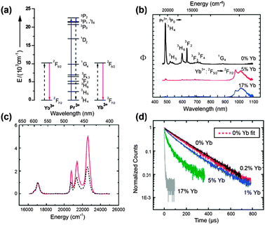
| Fig. 18 (a) Representative excitation spectra for YAG:Ce3+,Yb3+ (Y2.91–3xCe0.09Yb3xAl5O12, x = 0.1) monitoring the emission of Ce3+ at 530 nm, and the emission of Yb3+ at 1030 nm, respectively. For comparison, the excitation spectra of Yb3+ of quantum-cutting materials activated with ion pairs of Yb3+–Ln3+ (Ln = Tb, Tm, and Pr; the host is a borogermanate glass) and Yb3+–Ce3+ (the host is a borate glass) are also given. The AM 1.5G solar spectrum in this spectral region is shown in the background as a reference. (b) Concentration-dependent emission spectra of YAG:Ce3+,Yb3+ (x = 0–0.5) and YAG:Yb3+ (Y2.7Yb0.3Al5O12) under the excitation at 470 nm. (Reprinted with permission from ref. 282. Copyright 2009, Optical Society of America.) | ||
Several groups also used the Ce3+ ion to sensitize the Tb3+–Yb3+ quantum-cutting process.285–287 A possible indirect ET mechanism was proposed for the Ce3+–Tb3+–Yb3+ quantum-cutting system. First, the Ce3+ ion directly absorbs an ultraviolet photon via allowed 4f–5d transitions. Subsequently, the excitation energy in the lowest 5d (Ce3+) excited level relaxes to the 5D3 and 5D4 (Tb3+) levels via phonon assistance. From the 5D4 level, the energy of the excited Tb3+ ion is simultaneously transferred to two different Yb3+ ions. The NIR emission of Yb3+ in the Ce3+–Tb3+–Yb3+ system can be enhanced by about 10 times as compared to that obtained with the Tb3+–Yb3+ couple. Nonetheless, the quantum-cutting mechanism in this triply doped system remains elusive. Further experimentation is clearly needed. Another interesting development of quantum-cutting is the work on sensitization of the Pr3+–Yb3+ couple using Ce3+ ions.308
In a following paper by Shestakov et al., Li+–Yb3+ co-doped ZnO nanocrystals were tested for NIR quantum-cutting.302 ZnO is a direct wide gap semiconductor with large absorption cross-section in the 250–400 nm ultraviolet wavelength range and high transparency in the visible and NIR ranges. Upon ultraviolet excitation, the authors observed two broadband emissions centered at 770 and 1000 nm, which can be ascribed to Li+–Li+ and Yb3+–Li+ dimer dopants, respectively. Pump power dependence and temperature dependence of these emission bands indicated that the ET from the ZnO host to Li+–Li+ and Yb3+–Li+ dimers was responsible for the quantum-cutting mechanism.
4.4 Quantum-cutting for germanium solar cells
The energy of the 4I13/2 → 4I15/2 transition of Er3+ around 1540 nm is slightly larger than the bandgap of germanium (0.67 eV; 1850 nm). To this end, the NIR quantum-cutting of Er3+ has potential to improve the efficiency of germanium-based solar cells. Chen et al. in 2009 reported three-photon NIR quantum-cutting of Er3+ in the GdVO4 crystal.240 Upon 523 nm excitation of Er3+ to the 2H11/2 level, they observed a characteristic NIR emission at 1532 nm due to 4I13/2 → 4I15/2 transition, with a quantum efficiency of about 178%. The principal drawback of this system is the low effective absorption cross-section of Er3+ at 300–550 nm. To solve this problem, Zhou et al.316,317 in 2010 demonstrated that the incorporation of Ce3+ and Eu2+ in YAG:Ce3+/Er3+ and Ca8Mg(SiO4)4Cl2:Eu2+/Er3+ phosphors results in strong erbium sensitization, leading to significantly increased NIR emission intensity of Er3+.Subsequently, two research groups independently reported a novel quantum-cutting mechanism based on resonant ET from Er3+ to Yb3+ in Er3+/Yb3+ co-doped glass ceramics and NaYF4 nanocrystals, respectively.318,319 In these systems, a photon, absorbed by Er3+ in the wavelength range of 350–550 nm, was converted into two photons of 650–1550 nm that can be subsequently emitted by Er3+ and Yb3+, with the maximum quantum efficiency approaching 200%.
4.5 Multiple exciton generation in quantum dots
Different from the above-mentioned quantum-cutting in lanthanide ions, another viable approach to significantly enhance solar energy conversion is to utilize multiple exciton generation (MEG, also termed carrier multiplication) in QDs, whereby the absorption of one photon bearing at least twice the bandgap energy can produce two or more electron–hole pairs (Fig. 19a).320–322 This approach enables effective harvesting of high-energy photons in the violet and ultraviolet parts of the solar spectrum that are normally lost as waste heat.323 Thus, the application of MEG in third-generation PV cells has the potential to achieve maximum efficiency as high as 44%, well exceeding the Shockley–Queisser limit of 31% for single-junction solar cells.324 Since its first discovery in PbSe nanocrystals by Schaller and Klimov in 2004,325 the MEG effect has been experimentally observed in many QD systems, such as PbS, PbTe, CdSe, and Si,326 as well as recently in single-walled carbon nanotubes.327,328 Several recent reviews have discussed the mechanisms, characterization techniques, and application prospects of the MEG effect, but problems and disagreements have arisen over the measurement of MEG quantum efficiency in colloidal QDs and its impact on solar energy conversion.329–334 Most of the previous studies have used ultrafast transient absorption techniques, as proposed by Schaller and Klimov,325 to measure the MEG efficiency, which is defined as the number of electron–hole pairs produced per absorbed photon. The indirect nature of this method, however, has contributed to the diversity in the reported experimental data resulting from experimental artefacts, material degradation and surface effects of carrier trapping and photocharging.335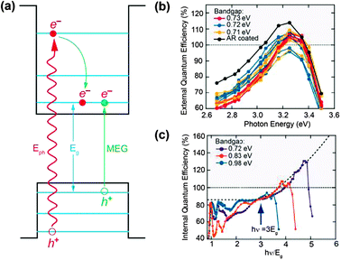 | ||
| Fig. 19 (a) A schematic drawing showing multiple exciton generation, whereby excited carriers generated in a quantum dot can channel excess photon energy to promote another electron across the bandgap rather than undergo thermalization. (b) External quantum efficiency measurements for 18 independent devices made with QD bandgaps of 0.71 eV (yellow), 0.72 eV (blue), and 0.73 eV (red), as well as a device with an antireflective coating (black). A maximum external quantum efficiency of up to 114% is achieved, confirming the generation of multiple excitons in QDs. (c) Collected internal quantum efficiency curves versus the ratio of photon energy to bandgap, hν/Eg, for three QD sizes. (Reprinted with permission from (a) ref. 320, (b) ref. 336, and (c) ref. 336. Copyright 2009 and 2011, respectively, Nature Publishing Group and American Association for the Advancement of Science.) | ||
In 2011, Semonin and colleagues demonstrated direct proof of carrier multiplication in QDs.336 They found that about 4% of total photocurrent in PbSe-based solar cells arises from the MEG effect. In such solar cells, the MEG was measured by determining the cell's external and internal quantum efficiencies at zero applied bias. In their work, a peak external quantum efficiency of 114% and a peak internal quantum efficiency of 130% were obtained (Fig. 19b and c). These findings are important because they not only provide direct evidence for MEG in QDs, but also show that MEG charge carriers can be collected with reasonable efficiency in suitably designed QD solar cells. Nevertheless, the impact of MEG on the power conversion efficiency of QD solar cells is limited, largely due to the high energy threshold of ∼3.0 Eg required for MEG in PbSe QDs (as shown in Fig. 19b, only ultraviolet photons can result in efficient MEG). To make MEG have a substantial impact on PV devices, QD-based solar cells that can generate multiple excitons per visible photon at wavelength near the solar peak need to be developed in the future.
5. Down-shifting materials for PV applications
5.1 Concepts of luminescent down-shifting
Luminescent down-shifting can be utilized in many PV devices that exhibit poor spectral response to short-wavelength light. The down-shifting materials absorb the short-wavelength light, typically in the 300–500 nm range, and re-emit it at a longer wavelength where the external quantum efficiency of the PV device is high. While luminescent down-shifting could potentially enhance the solar cell efficiency, it is important to note that the design will not be able to overcome the Shockley–Queisser efficiency limit, as the absorption of a high energy photon by the down-shifting materials can only result in the generation of one electron–hole pair in the solar cell. To date, two main classes of down-shifting-based PV devices have been investigated: luminescent solar concentrators and planar down-shifting layers.337 A luminescent solar concentrator is used to concentrate sunlight onto PV cells as a simple means to reduce the amount of expensive PV materials required.338,339 The concentrator, typically composed of polymer sheets doped with luminescent species, converts a fraction of the incident sunlight into longer wavelength light that is subsequently guided towards a PV cell (Fig. 20a).340,341 On the other hand, a planar down-shifting layer is generally placed directly onto the front surface of a solar cell to improve the device performance by overcoming the poor spectral response of the solar cell to short-wavelength light (Fig. 20b).342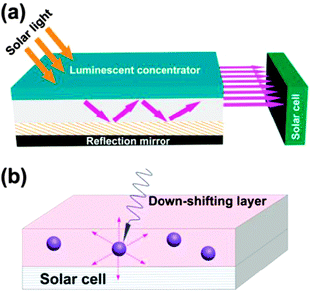 | ||
| Fig. 20 (a) Schematic design of a solar cell device equipped with a luminescent solar concentrator. The solar concentrator consists of a flat transparent slab with embedded luminescent down-shifting materials. The luminescent material absorbs incoming solar light and re-emits it at a longer wavelength isotropically. The emitted light, trapped in the slab via total internal reflection, is then guided to solar cells placed next to the edge of the slab. (b) Schematic design of a solar cell device with a luminescent down-shifting layer directly placed onto the surface of the solar cell. The down-shifting layer absorbs short wavelength photons and then re-emits them at a longer wavelength where the device exhibits a better spectral response. | ||
The ideal materials for luminescent down-shifting should possess the following characteristics: (i) broadband absorption, particularly in the region where the spectral response of the solar cell is low; (ii) high absorption coefficient and high luminescence quantum efficiency so that all incident light results in emission; (iii) high transmittance and narrowband emission, particularly in the region where the device response is high; (iv) large Stokes shift to minimize the self-absorption energy losses due to the spectral overlap between the absorption and emission bands; and (v) long-term stability.343 Up to now, inorganic phosphors and glasses, colloidal QDs and organolanthanide complexes have been widely investigated as potential candidates, as will be discussed below.
5.2 Phosphors and glasses
Table 5 summarizes the recent development of phosphors and glasses as down-shifting layers for a variety of PV devices (e.g., c-Si, DSSCs, organic, and GaSb solar cells).297,344–371 In these studies, the principal strategy has been to convert the ultraviolet–blue radiation into red–NIR emission by utilizing Stokes-shifted photoluminescence.| Materials | Preparation method | Excitation (nm) | Emission (nm) | Solar cell type | Ref. |
|---|---|---|---|---|---|
| Y2O3:Eu3+ | — | 250 | 570–700 | c-Si | 344 |
| La2O3:Eu3+ | Sol–gel Pechini method | 285 | 570–700 | c-Si | 345 |
| YVO4:Bi3+,Eu3+ thin films | Aqueous precipitation | 250–400 | 570–700 | c-Si | 346 |
| YAG:Ce3+,Cr3+ | Solid-state reaction | 400–500 | 688 | c-Si | 347 |
| MgSrAl10O17:Eu2+,Cr3+ | Solid-state reaction | 250–450 | 693 | c-Si | 348 |
| SrB4O7:5%Sm2+,5%Eu2+ | Solid-state reaction | 300–600 | 685 | c-Si | 371 |
| YAG:Ce3+,Nd3+ | Co-precipitation | 400–500 | 888, 1064 | c-Si | 349 |
| YAG:Ce3+,Nd3+ | Sol–gel | 400–500 | 850–950, 1062 | c-Si | 350 |
| Cr3+–Yb3+ co-doped fluorosilicate glass | Glass melting | 300–700 | 950–1100 | c-Si | 351 |
| ZnO–LiYbO2 hybrid phosphors | Solid-state reaction | 200–400 | 950–1100 | c-Si | 352, 353 |
| Yb3+-doped glass ceramics containing ZnO nanocrystals | Glass melting | 200–400 | 950–1100 | c-Si | 354 |
| LiYbMo2O8:Pb2+ | Solid-state reaction | 300–450 | 950–1100 | c-Si | 355 |
| CaLaGa3S6O:Yb3+ | Solid-state reaction | 250–500 | 950–1100 | c-Si | 356 |
| Yb3+ doped LaSi3N5 | Solid-state reaction | 300–400 | 950–1100 | c-Si | 357 |
| Ag nanoclusters and Yb3+ ions co-doped oxyfluoride glasses | Glass melting | 300–500 | 950–1100 | c-Si | 358 |
| Yb3+-doped glass ceramics containing Ba2TiSi2O8 nanocrystals | Glass melting | 250–350 | 950–1100 | c-Si | 359 |
| Yb3+-doped SrO–TiO2–SiO2 glasses | Glass melting | 250–350 | 950–1100 | c-Si | 360 |
| Dy3+–Tb3+ co-doped glass ceramics containing YF3 nanocrystals | Glass melting | 300–500 | 450–650 | c-Si | 361 |
| Cu+ doped glasses | Glass melting | 250–320 | 495 | c-Si | 362 |
| Tb3+ doped glasses | Glass melting | 300–400 | 520–700 | Thin film | 363 |
| LaVO4:Dy3+ | Hydrothermal method | 250–320 | 450–600 | DSSCs | 364 |
| Y2O3:Eu3+ | Co-precipitation | 230–320 | 570–700 | DSSCs | 365 |
| TiO2:Ln3+ (Ln = Eu, Sm) | Sol–gel | 200–400 | 570–700 | DSSCs | 366, 367 |
| YVO4:Bi3+,Ln3+ (Ln = Eu, Sm) | Solid-state reaction | 250–400 | 570–700 | DSSCs | 297 |
| LaOF:Eu3+ | Hydrothermal method | 325–550 | 570–700 | Organic | 368 |
| YVO4:Bi3+,Eu3+ thin films | Solid-state reaction | 250–400 | 570–700 | Organic | 369 |
| Bismuth-doped oxide glasses | Glass melting | 300–800 | 1000–1600 | GaSb | 370 |
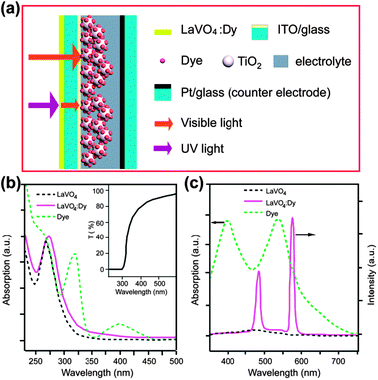 | ||
| Fig. 21 (a) Structure of a DSSC coupled with the LaVO4:Dy3+ ultraviolet-filtering thin-film. Note that ultraviolet light could be absorbed and converted to visible light via the thin-film. (b) The absorption spectrum of LaVO4:Dy3+ nanocrystals compared with the absorption spectrum of N3 dye. Inset: the transmittance spectrum of the LaVO4:Dy3+ thin-film. (c) The emission spectrum of LaVO4:Dy3+ nanocrystals compared with the absorption spectrum of N3 dye. (Reprinted with permission from ref. 364. Copyright 2006, American Institute of Physics.) | ||
In 2011, Hafez et al.366 reported the fabrication of lanthanide-doped TiO2 photoelectrodes that are used to boost the conversion efficiency of DSSCs. Efficiency as high as 5.81% and 5.16% was reported for Sm3+ and Eu3+, respectively. In contrast, the undoped titania photoelectrodes only yielded 4.23% efficiency. The higher improvement with the Sm3+ dopant in the overall efficiency of the solar cells was attributed to the smaller lifetime values of Sm3+ than that of Eu3+. Due to efficient host-to-Sm3+ ET, the Sm3+-doped TiO2 thin films exhibited a characteristic orange-red emission upon excitation in the range of 250–400 nm. The orange-red emission was then absorbed by a sensitizing ruthenium dye N719 [RuL2(NCS)2, L = 4,4-dicarboxylate-2,2-bipyridine]. With further device optimization and new dyes (e.g., N749), much higher efficiencies are likely.
5.3 Semiconductor quantum dots
Semiconductor QDs are a different class of luminescent down-shifting materials that have been recently reported for solar cell applications. In particular, CdSe, CdSe–ZnS, CdS, and CdSe–CdTe have generated great excitement because they feature broadband absorbance, high quantum yield, and tunable emission characteristics in the visible region.386–401 However, the overall efficiencies of these solar cells need to be improved due to large overlap between the emission and absorption spectra of the QDs.402,403 In contrast, the use of NIR-emitting QDs (e.g., Ag2S,404 PbS,405 ZnTe–CdSe,406 CdSe–ZnTe,407 and CdTe–CdSe408) can greatly reduce re-absorption. As an added benefit, the NIR emission of QDs can be tuned to match the bandgap of c-Si solar cells, thereby opening the possibility of developing luminescent solar concentrators with much higher conversion efficiency.In 2010, Shcherbatyuk et al. investigated the viability of using PbS NIR-emitting QDs as down-shifting materials in luminescent solar concentrators.402 When compared with CdSe–ZnS, the PbS QDs exhibited a broad spectral response extending from the visible to the NIR region of the solar spectrum (Fig. 22). Furthermore, the PbS QDs showed a large Stokes shift of 122 nm (versus 23 nm for CdSe–ZnS QDs) due to a strong quantum confinement effect. More importantly, the authors found that the NIR emission wavelength of the QDs is slightly larger than the bandgap of c-Si (1.1 eV), achieving calculated optical and power conversion efficiency in the luminescent solar concentrator as high as 12.6% and 3.2%, respectively.
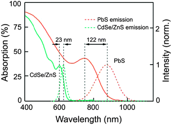 | ||
| Fig. 22 Comparison of absorption and emission spectra of CdSe–ZnS and PbS QDs. The Stokes shifts for CdSe–ZnS and PbS QDs are 23 and 122 nm, respectively. (Reprinted with permission from ref. 402. Copyright 2009, American Institute of Physics.) | ||
5.4 Rare-earth organic complexes
Rare-earth organic complexes, composed of a ligand acting as an antenna (or sensitizer) and an emitting lanthanide ion, are an important class of down-shifting materials for PV modules. Unlike conventional organic dyes and QDs, these organolanthanide complexes feature large Stokes shift and completely avoid self-absorption losses (Fig. 23a).409–411 In principle, the luminescence process in organolanthanide complexes occurs in three steps: (i) light absorption by a properly selected ligand; (ii) highly efficient intra-energy conversion from the singlet (S1) to the triplet (T1) states of the ligand by inter-system crossing; and (iii) resonant ET from the T1 state of the ligand to the excited state of the Ln3+ ion (Fig. 23b). Europium complexes that feature a main emission at 612 nm have been investigated for c-Si and DSSCs.412–420 In contrast, Tb3+-based organic complexes are more suitable for amorphous Si solar cells with a wavelength of maximum efficiency at about 500 nm.421,422 In particular, NIR-emitting metal–organic frameworks that contain Yb3+ or Nd3+ are promising candidates for c-Si solar cells.423–426 It is important to note that the organolanthanide complexes with high luminescence quantum efficiency and a broad absorption plateau in the visible region are preferred for PV applications.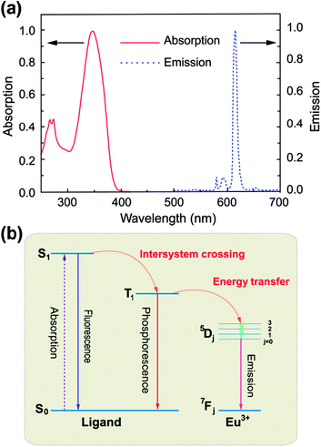 | ||
| Fig. 23 (a) Normalized absorption (solid line) and emission spectra (dashed line) of Eu(TTA)3(TTPO)2 where TTA and TTPO stand for thenoyl trifluoroacetone and triphenyl phosphine oxide, respectively. (b) Schematic diagram showing the ET process from the organic ligand to Eu3+ in organometallic compounds of europium. (Reprinted with permission from ref. 410. Copyright 2011, Elsevier Ltd.) | ||
6. Conclusions and outlook
In this review, fundamentals for luminescent materials as spectral converters are presented in the context of enhancing solar cell efficiency. One of the major challenges in designing solar cell devices is how to minimize energy losses due to the spectral mismatch between the solar cell and incident solar spectrum. To make full use of the solar spectrum, innovative approaches through use of upconversion, quantum-cutting, and down-shifting luminescent materials, albeit still very much in its infancy stage, have shown promise for the development of these materials as spectral converters to effectively reduce the spectral mismatch losses and, as a consequence, boost the efficiency of solar cells.Upconversion is able to harvest the sub-bandgap sunlight. Proof-of-concept experiments have been widely performed for Er3+-doped upconverters (for c-Si solar cells) and Ln3+–Yb3+ (Ln = Er, Tm, and Ho) co-doped upconverters (for wide bandgap solar cells). However, two major drawbacks associated with this approach currently limit the practical application of upconverters for solar cells. First, the efficiency of current Ln3+-doped upconverters investigated for solar cells is generally low (less than 3%).194 The upconversion efficiency may be enhanced by using plasmonic resonance427 or photonic crystals.428 High excitation density, which can be easily realized using lasers, also can lead to high upconversion efficiency, but it will require concentrated sunlight. In this respect, low-power TTA-based upconversion in organic molecules is particularly promising for wide bandgap solar cells, provided that efficient NIR-to-visible upconversion can be achieved.197,198 Second, only a small fraction of sub-bandgap sunlight can be upconverted due to the small absorption cross-sections of Ln3+ ions. Transition metal ions,429 quantum dots,430 and organic dyes431 with large absorption cross-sections might be exploited as sensitizers to enable broadband absorption of Ln3+ ions.
Quantum-cutting allows the efficient use of the high-energy above-bandgap sunlight, which provides potential for efficiency enhancement of narrow bandgap solar cells (c-Si solar cells and germanium solar cells). Efficient narrow-band NIR quantum-cutting with internal quantum efficiency close to 200% has been extensively demonstrated in the Ln3+–Yb3+ (Ln = Tb, Tm, Pr, Er, Nd, Ho, and Dy) couples for c-Si solar cells. In these couples, Yb3+ ions function as ideal acceptors with a single NIR emission band around 1000 nm, just above the bandgap of c-Si. To solve the absorption problem inherent in Ln3+ donors, other species (e.g., Ce3+, Eu2+, Yb2+, and Bi3+ ions) or hosts have been explored for sensitization. NIR quantum-cutting with Ce3+–Er3+ and Eu2+–Er3+ couples, which can give rise to NIR emission around 1500 nm from Er3+ donors, has been reported for germanium solar cells. Quantum-cutting has been proven to be a linear process independent of the incident power. This allows for the use of non-concentrated sunlight. However, quantum-cutting with external quantum efficiency larger than 100% has been rarely reported.432 Thus far, no proof-of-concept experiment has been reported for quantum-cutting in PV applications. Urgent tasks for the distant future in this area are: (i) developing novel characterization techniques to provide direct evidence of the existence of NIR quantum-cutting; and (ii) investigating the effect of quantum-cutting materials on the performance of solar cells.
Down-shifting offers the ability to improve the spectral response of solar cells to short-wavelength sunlight. Lanthanide-doped phosphors and glasses, QDs, and organolanthanide complexes can be used in luminescent solar concentrators and planar down-shifting layers for enhancing power-conversion efficiency in solar cells. However, the fabrication of a highly efficient luminescent solar concentrator remains difficult,433 and the optimal configuration may involve a combination or design layout of different luminescent materials.434,435
In conclusion, the application of luminescent materials as spectral converters to PV applications could not come at a more opportune time given the significant increase in the global demand for energy in recent years. Despite the daunting challenges of realizing low-cost and highly efficient solar cells, further exploration and attempts to use these spectral converting materials for PV devices and systems will certainly be exciting.
Acknowledgements
X.L. acknowledges the National Research Foundation and the Economic Development Board (Singapore-Peking-Oxford Research Enterprise, COY-15-EWI-RCFSA/N197-1), the Singapore-MIT Alliance, the Ministry of Education (MOE2010-t2-1-083), and the Agency for Science, Technology and Research (A*STAR) for supporting this work. W.H. acknowledges financial support from National Basic Research Program of China (973 Program, 2009CB930601), National Natural Science Foundation of China (BZ2010043, 20974046, 20774043, 51173081, 50428303, 61136003) and Natural Science Foundation of Jiangsu Province (BK2008053, BK2009025, 10KJB510013).References
- G. D. Scholes, G. R. Fleming, A. Olaya-Castro and R. van Grondelle, Nat. Chem., 2011, 3, 763–774 CrossRef CAS.
- N. S. Lewis, Science, 2007, 315, 798–801 CrossRef CAS.
- H. Aguas, S. K. Ram, A. Araujo, D. Gaspar, A. Vicente, S. A. Filonovich, E. Fortunato, R. Martins and I. Ferreira, Energy Environ. Sci., 2011, 4, 4620–4632 CAS.
- H. A. Atwater and A. Polman, Nat. Mater., 2010, 9, 205–213 CrossRef CAS.
- A. J. Nozik and J. Miller, Chem. Rev., 2010, 110, 6443–6445 CrossRef CAS.
- P. K. Nayak, G. Garcia-Belmonte, A. Kahn, J. Bisquert and D. Cahen, Energy Environ. Sci., 2012, 5, 6022–6039 CAS.
- W. Y. Wong and C. L. Ho, Acc. Chem. Res., 2010, 43, 1246–1256 CrossRef CAS.
- J. D. Servaites, M. A. Ratner and T. J. Marks, Energy Environ. Sci., 2011, 4, 4410–4422 CAS.
- A. Yella, H. W. Lee, H. N. Tsao, C. Y. Yi, A. K. Chandiran, M. K. Nazeeruddin, E. W. G. Diau, C. Y. Yeh, S. M. Zakeeruddin and M. Gratzel, Science, 2011, 334, 629–634 CrossRef CAS.
- M. D. Kelzenberg, S. W. Boettcher, J. A. Petykiewicz, D. B. Turner-Evans, M. C. Putnam, E. L. Warren, J. M. Spurgeon, R. M. Briggs, N. S. Lewis and H. A. Atwater, Nat. Mater., 2010, 9, 239–244 CrossRef CAS.
- X. H. Wang, G. I. Koleilat, J. Tang, H. Liu, I. J. Kramer, R. Debnath, L. Brzozowski, D. A. R. Barkhouse, L. Levina, S. Hoogland and E. H. Sargent, Nat. Photonics, 2011, 5, 480–484 CrossRef CAS.
- K. Q. Peng and S. T. Lee, Adv. Mater., 2011, 23, 198–215 CrossRef CAS.
- A. I. Hochbaum and P. D. Yang, Chem. Rev., 2010, 110, 527–546 CrossRef CAS.
- D. Timmerman, I. Izeddin, P. Stallinga, I. N. Yassievich and T. Gregorkiewicz, Nat. Photonics, 2008, 2, 105–109 CrossRef CAS.
- B. E. Hardin, H. J. Snaith and M. D. McGehee, Nat. Photonics, 2012, 6, 162–169 CrossRef CAS.
- J. W. Schwede, I. Bargatin, D. C. Riley, B. E. Hardin, S. J. Rosenthal, Y. Sun, F. Schmitt, P. Pianetta, R. T. Howe, Z. X. Shen and N. A. Melosh, Nat. Mater., 2010, 9, 762–767 CrossRef CAS.
- N. C. Giebink, G. P. Wiederrecht and M. R. Wasielewski, Nat. Photonics, 2011, 5, 695–702 CrossRef.
- P. V. Kamat, K. Tvrdy, D. R. Baker and J. G. Radich, Chem. Rev., 2010, 110, 6664–6688 CrossRef CAS.
- S. Chu and A. Majumdar, Nature, 2012, 488, 294–303 CrossRef CAS.
- M. Graetzel, R. A. J. Janssen, D. B. Mitzi and E. H. Sargent, Nature, 2012, 488, 304–312 CrossRef CAS.
- B. S. Richards, Sol. Energy Mater. Sol. Cells, 2006, 90, 2329–2337 CrossRef CAS.
- W. Shockley and H. J. Queisser, J. Appl. Phys., 1961, 32, 510–519 CrossRef CAS.
- C. Strumpel, M. McCann, G. Beaucarne, V. Arkhipov, A. Slaoui, V. Svrcek, C. del Canizo and I. Tobias, Sol. Energy Mater. Sol. Cells, 2007, 91, 238–249 CrossRef.
- B. S. Richards, Sol. Energy Mater. Sol. Cells, 2006, 90, 1189–1207 CrossRef CAS.
- A. Shalav, B. S. Richards and M. A. Green, Sol. Energy Mater. Sol. Cells, 2007, 91, 829–842 CrossRef CAS.
- T. Trupke, A. Shalav, B. S. Richards, P. Wurfel and M. A. Green, Sol. Energy Mater. Sol. Cells, 2006, 90, 3327–3338 CrossRef CAS.
- G. Conibeer, Mater. Today, 2007, 10, 42–50 CrossRef CAS.
- G. F. Brown and J. Q. Wu, Laser Photonics Rev., 2009, 3, 394–405 CrossRef CAS.
- S. V. Eliseeva and J. C. G. Bunzli, Chem. Soc. Rev., 2010, 39, 189–227 RSC.
- D. Chen, Y. Wang and M. Hong, Nano Energy, 2012, 1, 73–90 CrossRef.
- B. M. van der Ende, L. Aarts and A. Meijerink, Phys. Chem. Chem. Phys., 2009, 11, 11081–11095 RSC.
- T. Trupke, M. A. Green and P. Wurfel, J. Appl. Phys., 2002, 92, 4117–4122 CrossRef CAS.
- Q. Y. Zhang and X. Y. Huang, Prog. Mater. Sci., 2010, 55, 353–427 CrossRef CAS.
- T. Trupke, M. A. Green and P. Wurfel, J. Appl. Phys., 2002, 92, 1668–1674 CrossRef CAS.
- J. Nelson, The Physics of Solar Cells, Imperial College Press, 2002 Search PubMed.
- D. M. Powell, M. T. Winkler, H. J. Choi, C. B. Simmons, D. B. Needleman and T. Buonassisi, Energy Environ. Sci., 2012, 5, 5874–5883 Search PubMed.
- M. A. Green, K. Emery, Y. Hishikawa and W. Warta, Prog. Photovoltaics, 2011, 19, 84–92 CAS.
- M. A. Green, K. Emery, Y. Hishikawa and W. Warta, Prog. Photovoltaics, 2010, 18, 346–352 Search PubMed.
- C. Feldmann, T. Justel, C. R. Ronda and P. J. Schmidt, Adv. Funct. Mater., 2003, 13, 511–516 CrossRef CAS.
- B. Valeur and M. N. Berberan-Santos, J. Chem. Educ., 2011, 88, 731–738 CrossRef CAS.
- G. Blasse and B. C. Grabmaier, Luminescent Materials, Springer, Berlin, 1994 Search PubMed.
- C. R. Ronda, in Luminescence From Theory to Applications, ed. C. R. Ronda, Wiley-VCH Verlag GmbH & Co. KGaA, Weinheim, 2008, pp. 1–34 Search PubMed.
- S. Kuck, I. Sokolska, M. Henke, T. Scheffler and E. Osiac, Phys. Rev. B: Condens. Matter., 2005, 71, 165112 CrossRef.
- L. S. Rohwer and J. E. Martin, J. Lumin., 2005, 115, 77–90 CrossRef CAS.
- M. H. V. Werts, R. T. F. Jukes and J. W. Verhoeven, Phys. Chem. Chem. Phys., 2002, 4, 1542–1548 RSC.
- K. Binnemans, Chem. Rev., 2009, 109, 4283–4374 CrossRef CAS.
- J. C. G. Bunzli, Acc. Chem. Res., 2006, 39, 53–61 CrossRef.
- J. C. G. Bunzli and C. Piguet, Chem. Soc. Rev., 2005, 34, 1048–1077 RSC.
- J. C. G. Bunzli, Chem. Rev., 2010, 110, 2729–2755 CrossRef.
- S. Ye, F. Xiao, Y. X. Pan, Y. Y. Ma and Q. Y. Zhang, Mater. Sci. Eng., R, 2010, 71, 1–34 CrossRef.
- T. Justel, H. Nikol and C. Ronda, Angew. Chem., Int. Ed., 1998, 37, 3085–3103 CrossRef.
- H. A. Hoppe, Angew. Chem., Int. Ed., 2009, 48, 3572–3582 CrossRef.
- L. D. Carlos, R. A. S. Ferreira, V. D. Bermudez, B. Julian-Lopez and P. Escribano, Chem. Soc. Rev., 2011, 40, 536–549 RSC.
- A. Kar and A. Patra, Nanoscale, 2012, 4, 3608–3619 RSC.
- H. Goesmann and C. Feldmann, Angew. Chem., Int. Ed., 2010, 49, 1362–1395 CrossRef CAS.
- G. H. Dieke, Spectra and Energy Levels of Rare Earth Ions in Crystals, Wiley, New York, 1968 Search PubMed.
- G. K. Liu, in Spectroscopic Properties of Rare Earths in Optical Materials, ed. G. K. Liu and B. Jacquier, Springer Verlag, Berlin, 2005, pp. 1–94 Search PubMed.
- M. F. H. Schuurmans and J. M. F. Vandijk, Physica B+C (Amsterdam), 1984, 123, 131–155 CAS.
- J. M. F. Vandijk and M. F. H. Schuurmans, J. Chem. Phys., 1983, 78, 5317–5323 CrossRef CAS.
- F. Vetrone and J. A. Capobianco, Int. J. Nanotechnol., 2008, 5, 1306–1339 CrossRef CAS.
- P. P. Fedorov, A. A. Luginina, S. V. Kuznetsov and V. V. Osiko, J. Fluorine Chem., 2011, 132, 1012–1039 CrossRef CAS.
- R. T. Wegh, H. Donker, K. D. Oskam and A. Meijerink, Science, 1999, 283, 663–666 CrossRef CAS.
- R. T. Wegh, H. Donker, K. D. Oskam and A. Meijerink, J. Lumin., 1999, 82, 93–104 CrossRef CAS.
- W. W. Piper and F. S. Ham, J. Lumin., 1974, 8, 344–348 CrossRef CAS.
- J. L. Sommerdijk, A. A. Bril and A. W. de Jager, J. Lumin., 1974, 8, 341–343 CrossRef CAS.
- J. L. Sommerdijk, A. Bril and A. W. de Jager, J. Lumin., 1974, 9, 288–296 CrossRef CAS.
- A. M. Srivastava and W. W. Beers, J. Lumin., 1997, 71, 285–290 CrossRef CAS.
- F. Auzel, in Spectroscopic Properties of Rare Earths in Optical Materials, ed. G. K. Liu and B. Jacquier, Springer Verlag, Berlin, 2005, pp. 266–319 Search PubMed.
- D. L. Dexter, J. Chem. Phys., 1953, 21, 836–850 CrossRef CAS.
- T. Miyakawa and D. L. Dexter, Phys. Rev. B: Solid State, 1970, 1, 2961–2969 CrossRef.
- N. Yamada, S. Shionoya and T. Kushida, J. Phys. Soc. Jpn., 1972, 32, 1577–1586 CrossRef CAS.
- F. Wang, D. Banerjee, Y. S. Liu, X. Y. Chen and X. G. Liu, Analyst, 2010, 135, 1839–1854 RSC.
- F. Wang and X. G. Liu, Chem. Soc. Rev., 2009, 38, 976–989 RSC.
- F. Auzel, Chem. Rev., 2004, 104, 139–173 CrossRef CAS.
- F. Wang, R. R. Deng, J. Wang, Q. X. Wang, Y. Han, H. M. Zhu, X. Y. Chen and X. G. Liu, Nat. Mater., 2011, 10, 968–973 CrossRef CAS.
- F. Wang, Y. Han, C. S. Lim, Y. H. Lu, J. Wang, J. Xu, H. Y. Chen, C. Zhang, M. H. Hong and X. G. Liu, Nature, 2010, 463, 1061–1065 CrossRef CAS.
- F. Wang and X. G. Liu, J. Am. Chem. Soc., 2008, 130, 5642–5643 CrossRef CAS.
- F. Wang, J. Wang and X. G. Liu, Angew. Chem., Int. Ed., 2010, 49, 7456–7460 CrossRef CAS.
- Y. M. Yang, Q. Shao, R. R. Deng, C. Wang, X. Teng, K. Cheng, Z. Cheng, L. Huang, Z. Liu, X. G. Liu and B. G. Xing, Angew. Chem., Int. Ed., 2012, 51, 3125–3129 CrossRef CAS.
- R. R. Deng, X. J. Xie, M. Vendrell, Y. T. Chang and X. G. Liu, J. Am. Chem. Soc., 2011, 133, 20168–20171 CrossRef CAS.
- J. Wang, F. Wang, C. Wang, Z. Liu and X. G. Liu, Angew. Chem., Int. Ed., 2011, 50, 10369–10372 CrossRef CAS.
- X. J. Xue, F. Wang and X. G. Liu, J. Mater. Chem., 2011, 21, 13107–13127 RSC.
- S. Ye, Y. J. Li, D. C. Yu, G. P. Dong and Q. Y. Zhang, J. Mater. Chem., 2011, 21, 3735–3739 RSC.
- E. Downing, L. Hesselink, J. Ralston and R. Macfarlane, Science, 1996, 273, 1185–1189 CAS.
- G. F. Wang, Q. Peng and Y. D. Li, Acc. Chem. Res., 2011, 44, 322–332 CrossRef CAS.
- L. H. Fischer, G. S. Harms and O. S. Wolfbeis, Angew. Chem., Int. Ed., 2011, 50, 4546–4551 CrossRef CAS.
- J. Zhou, Z. Liu and F. Y. Li, Chem. Soc. Rev., 2012, 41, 1323–1349 RSC.
- C. X. Li and J. Lin, J. Mater. Chem., 2010, 20, 6831–6847 RSC.
- M. Haase and H. Schafer, Angew. Chem., Int. Ed., 2011, 50, 5808–5829 CrossRef CAS.
- Q. Ju, D. T. Tu, Y. S. Liu, R. F. Li, H. M. Zhu, J. C. Chen, Z. Chen, M. D. Huang and X. Y. Chen, J. Am. Chem. Soc., 2012, 134, 1323–1330 CrossRef CAS.
- D. T. Tu, L. Q. Liu, Q. Ju, Y. S. Liu, H. M. Zhu, R. F. Li and X. Y. Chen, Angew. Chem., Int. Ed., 2011, 50, 6306–6310 CrossRef CAS.
- H. S. Mader, P. Kele, S. M. Saleh and O. S. Wolfbeis, Curr. Opin. Chem. Biol., 2010, 14, 582–596 CrossRef CAS.
- C. Yan, A. Dadvand, F. Rosei and D. F. Perepichka, J. Am. Chem. Soc., 2010, 132, 8868–8869 CrossRef CAS.
- N. Bogdan, F. Vetrone, G. A. Ozin and J. A. Capobianco, Nano Lett., 2011, 11, 835–840 CrossRef CAS.
- X. C. Ye, J. E. Collins, Y. J. Kang, J. Chen, D. T. N. Chen, A. G. Yodh and C. B. Murray, Proc. Natl. Acad. Sci. U. S. A., 2010, 107, 22430–22435 CrossRef CAS.
- O. Ehlert, R. Thomann, M. Darbandi and T. Nann, ACS Nano, 2008, 2, 120–124 CrossRef CAS.
- F. Chen, W. B. Bu, S. J. Zhang, X. H. Liu, J. N. Liu, H. Y. Xing, Q. F. Xiao, L. P. Zhou, W. J. Peng, L. Z. Wang and J. L. Shi, Adv. Funct. Mater., 2011, 21, 4285–4294 CrossRef CAS.
- G. S. Yi and G. M. Chow, Chem. Mater., 2007, 19, 341–343 CrossRef CAS.
- F. Zhang, G. B. Braun, A. Pallaoro, Y. Zhang, Y. Shi, D. Cui, M. Moskovits, D. Zhao and G. D. Stucky, Nano Lett., 2012, 12, 61–67 CrossRef CAS.
- L. Cheng, K. Yang, Y. G. Li, X. Zeng, M. W. Shao, S. T. Lee and Z. Liu, Biomaterials, 2012, 33, 2215–2222 CrossRef CAS.
- C. Bouzigues, T. Gacoin and A. Alexandrou, ACS Nano, 2011, 5, 8488–8505 CrossRef CAS.
- M. K. G. Jayakumar, N. M. Idris and Y. Zhang, Proc. Natl. Acad. Sci. U. S. A., 2012, 109, 8483–8488 CrossRef CAS.
- G. Lu, S. Z. Li, Z. Guo, O. K. Farha, B. G. Hauser, X. Y. Qi, Y. Wang, X. Wang, S. Y. Han, X. G. Liu, J. S. DuChene, H. Zhang, Q. C. Zhang, X. D. Chen, J. Ma, S. C. J. Loo, W. D. Wei, Y. H. Yang, J. T. Hupp and F. W. Huo, Nat. Chem., 2012, 4, 310–316 CrossRef CAS.
- J. C. Zhou, Z. L. Yang, W. Dong, R. J. Tang, L. D. Sun and C. H. Yan, Biomaterials, 2011, 32, 9059–9067 CrossRef CAS.
- H. Schafer, P. Ptacek, H. Eickmeier and M. Haase, Adv. Funct. Mater., 2009, 19, 3091–3097 CrossRef.
- H. Schafer, P. Ptacek, O. Zerzouf and M. Haase, Adv. Funct. Mater., 2008, 18, 2913–2918 CrossRef.
- H. Schaefer, P. Ptacek, K. Koempe and M. Haase, Chem. Mater., 2007, 19, 1396–1400 CrossRef CAS.
- G. Tian, Z. J. Gu, L. J. Zhou, W. Y. Yin, X. X. Liu, L. Yan, S. Jin, W. L. Ren, G. M. Xing, S. J. Li and Y. L. Zhao, Adv. Mater., 2012, 24, 1226–1231 CrossRef CAS.
- C. H. Dong, A. Korinek, B. Blasiak, B. Tomanek and F. C. J. M. van Veggel, Chem. Mater., 2012, 24, 1297–1305 CrossRef CAS.
- N. J. J. Johnson, A. Korinek, C. Dong and F. C. J. M. van Veggel, J. Am. Chem. Soc., 2012, 134, 11068–11071 CrossRef CAS.
- G. Y. Chen, H. L. Qiu, R. W. Fan, S. W. Hao, S. Tan, C. H. Yang and G. Han, J. Mater. Chem., 2012, 22, 20190–20196 RSC.
- G. Y. Chen, T. Y. Ohulchanskyy, A. Kachynski, H. Agren and P. N. Prasad, ACS Nano, 2011, 5, 4981–4986 CrossRef CAS.
- S. J. Zeng, J. J. Xiao, Q. B. Yang and J. H. Hao, J. Mater. Chem., 2012, 22, 9870–9874 RSC.
- W. L. Ren, G. Tian, L. J. Zhou, W. Y. Yin, L. Yan, S. Jin, Y. Zu, S. J. Li, Z. J. Gu and Y. L. Zhao, Nanoscale, 2012, 4, 3754–3760 RSC.
- E. M. Chan, G. Han, J. D. Goldberg, D. J. Gargas, A. D. Ostrowski, P. J. Schuck, B. E. Cohen and D. J. Milliron, Nano Lett., 2012, 3839–3845 CrossRef CAS.
- F. Chen, S. J. Zhang, W. B. Bu, Y. Chen, Q. F. Xiao, J. A. Liu, H. Y. Xing, L. P. Zhou, W. J. Peng and J. L. Shi, Chem.–Eur. J., 2012, 18, 7082–7090 CAS.
- Y. Wei, Q. Chen, B. Wu, A. Zhou and D. Xing, Nanoscale, 2012, 4, 3901–3909 RSC.
- S. J. Wu, N. Duan, X. Y. Ma, Y. Xia, Y. Yu, Z. P. Wang and H. X. Wang, Chem. Commun., 2012, 48, 4866–4868 RSC.
- T. He, W. Wei, L. Ma, R. Chen, S. Wu, H. Zhang, Y. Yang, J. Ma, L. Huang, G. G. Gurzadyan and H. Sun, Small, 2012, 8, 2163–2168 CrossRef CAS.
- L. L. Li, R. B. Zhang, L. L. Yin, K. Z. Zheng, W. P. Qin, P. R. Selvin and Y. Lu, Angew. Chem., Int. Ed., 2012, 51, 6121–6125 CrossRef CAS.
- X. Teng, Y. Zhu, W. Wei, S. Wang, J. Huang, R. Naccache, W. Hu, A. I. Y. Tok, Y. Han, Q. Zhang, Q. Fan, W. Huang, J. A. Capobianco and L. Huang, J. Am. Chem. Soc., 2012, 134, 8340–8343 CrossRef CAS.
- W. Wei, T. He, X. Teng, S. Wu, L. Ma, H. Zhang, J. Ma, Y. Yang, H. Chen, Y. Han, H. Sun and L. Huang, Small, 2012, 8, 2271–2276 CrossRef CAS.
- G. Dong, B. Chen, X. Xiao, G. Chai, Q. Liang, M. Peng and J. Qiu, Nanoscale, 2012, 4, 4658–4666 RSC.
- Q. Liu, Y. Sun, T. S. Yang, W. Feng, C. G. Li and F. Y. Li, J. Am. Chem. Soc., 2011, 133, 17122–17125 CrossRef CAS.
- D. Chen, Y. Yu, F. Huang, H. Lin, P. Huang, A. Yang, Z. Wang and Y. Wang, J. Mater. Chem., 2012, 22, 2632–2640 RSC.
- D. Chen, Y. Yu, F. Huang, P. Huang, A. Yang and Y. Wang, J. Am. Chem. Soc., 2010, 132, 9976–9978 CrossRef CAS.
- X. J. Zhu, J. Zhou, M. Chen, M. Shi, W. Feng and F. Y. Li, Biomaterials, 2012, 33, 4618–4627 CrossRef CAS.
- Y. F. Wang, L. D. Sun, J. W. Xiao, W. Feng, J. C. Zhou, J. Shen and C. H. Yan, Chem.–Eur. J., 2012, 18, 5558–5564 CrossRef CAS.
- F. Ferraro and C. Z. Hadad, J. Phys. Chem. C, 2012, 116, 7134–7143 CAS.
- F. Wang, J. Wang, J. Xu, X. J. Xue, H. Y. Chen and X. G. Liu, Spectrosc. Lett., 2010, 43, 400–405 CrossRef CAS.
- J. Wang, F. Wang, J. Xu, Y. Wang, Y. S. Liu, X. Y. Chen, H. Y. Chen and X. G. Liu, C. R. Chim., 2010, 13, 731–736 CrossRef CAS.
- S. Schietinger, T. Aichele, H. Q. Wang, T. Nann and O. Benson, Nano Lett., 2010, 10, 134–138 CrossRef CAS.
- J. H. Hao, Y. Zhang and X. H. Wei, Angew. Chem., Int. Ed., 2011, 50, 6876–6880 CrossRef CAS.
- A. X. Yin, Y. W. Zhang, L. D. Sun and C. H. Yan, Nanoscale, 2010, 2, 953–959 RSC.
- C. Zhang, H. P. Zhou, L. Y. Liao, W. Feng, W. Sun, Z. X. Li, C. H. Xu, C. J. Fang, L. D. Sun, Y. W. Zhang and C. H. Yan, Adv. Mater., 2010, 22, 633–637 CrossRef CAS.
- G. A. Jia, H. P. You, Y. H. Song, Y. J. Huang, M. Yang and H. J. Zhang, Inorg. Chem., 2010, 49, 7721–7725 CrossRef CAS.
- S. Wang, S. Q. Su, S. Y. Song, R. P. Deng and H. J. Zhang, CrystEngComm, 2012, 14, 4266–4269 RSC.
- M. F. Joubert, Opt. Mater. (Amsterdam), 1999, 11, 181–203 CAS.
- J. S. Chivian, W. E. Case and D. D. Eden, Appl. Phys. Lett., 1979, 35, 124–125 CrossRef CAS.
- P. Gibart, F. Auzel, J. C. Guillaume and K. Zahraman, Jpn. J. Appl. Phys., Part 1, 1996, 35, 4401–4402 CrossRef CAS.
- A. Shalav, B. S. Richards, T. Trupke, K. W. Kramer and H. U. Gudel, Appl. Phys. Lett., 2005, 86, 013505 CrossRef.
- S. Fischer, J. C. Goldschmidt, P. Loper, G. H. Bauer, R. Bruggemann, K. Kramer, D. Biner, M. Hermle and S. W. Glunz, J. Appl. Phys., 2010, 108, 044912 CrossRef.
- S. Ivanova, F. Pelle, A. Tkachuk, M. F. Joubert, Y. Guyot and V. P. Gapontzev, J. Lumin., 2008, 128, 914–917 CrossRef CAS.
- X. F. Liang, X. Y. Huang and Q. Y. Zhang, J. Fluoresc., 2009, 19, 285–289 CrossRef CAS.
- X. F. Wang, X. H. Yan and C. X. Kan, J. Mater. Chem., 2011, 21, 4251–4256 RSC.
- S. Ivanova and F. Pelle, J. Opt. Soc. Am. B, 2009, 26, 1930–1938 CrossRef CAS.
- F. Lahoz, Opt. Lett., 2008, 33, 2982–2984 CrossRef CAS.
- F. Lahoz, C. Perez-Rodriguez, S. E. Hernandez, I. R. Martin, V. Lavin and U. R. Rodriguez-Mendoza, Sol. Energy Mater. Sol. Cells, 2011, 95, 1671–1677 CrossRef CAS.
- H.-Y. Lin, H.-N. Chen, T.-H. Wu, C.-S. Wu, Y.-K. Su and S.-Y. Chu, J. Am. Ceram. Soc., 2012, 95, 3172–3179 CrossRef.
- X. D. Zhang, X. Jin, D. F. Wang, S. Z. Xiong, X. H. Geng and Y. Zhao, Phys. Status Solidi C, 2010, 7, 1128–1131 CAS.
- J. de Wild, A. Meijerink, J. K. Rath, W. G. J. H. M. van Sark and R. E. I. Schropp, Sol. Energy Mater. Sol. Cells, 2010, 94, 1919–1922 CrossRef CAS.
- J. de Wild, J. K. Rath, A. Meijerink, W. G. J. H. M. van Sark and R. E. I. Schropp, Sol. Energy Mater. Sol. Cells, 2010, 94, 2395–2398 CrossRef CAS.
- Z. Q. Li, X. D. Li, Q. Q. Liu, X. H. Chen, Z. Sun, C. Liu, X. J. Ye and S. M. Huang, Nanotechnology, 2012, 23, 025402 CrossRef CAS.
- S. L. Zhao, S. Q. Xu, G. H. Jia, D. G. Deng, L. H. Huang and H. P. Wang, Mater. Lett., 2011, 65, 2407–2409 CrossRef CAS.
- J. Wang, J. Wu, J. Lin, M. Huang, Y. Huang, Z. Lan, Y. Xiao, G. Yue, S. Yin and T. Sato, ChemSusChem, 2012, 5, 1307–1312 CrossRef CAS.
- G. B. Shan and G. P. Demopoulos, Adv. Mater., 2010, 22, 4373–4377 CrossRef CAS.
- G. B. Shan, H. Assaaoudi and G. P. Demopoulos, ACS Appl. Mater. Interfaces, 2011, 3, 3239–3243 CAS.
- A. F. Khan, R. Yadav, P. K. Mukhopadhya, S. Singh, C. Dwivedi, V. Dutta and S. Chawla, J. Nanopart. Res., 2011, 13, 6837–6846 CrossRef CAS.
- J. H. Wu, J. L. Wang, J. M. Lin, Z. Lan, Q. W. Tang, M. L. Huang, Y. F. Huang, L. Q. Fan, Q. B. Li and Z. Y. Tang, Adv. Energy Mater., 2012, 2, 78–81 CrossRef CAS.
- M. Liu, Y. Lu, Z. B. Xie and G. M. Chow, Sol. Energy Mater. Sol. Cells, 2011, 95, 800–803 CrossRef CAS.
- Q. Li, J. Lin, J. Wu, Z. Lan, Y. Wang, F. Peng and M. Huang, Electrochim. Acta, 2011, 56, 4980–4984 CrossRef CAS.
- V. D. Rodriguez, J. Mendez-Ramos, V. K. Tikhomirov, J. del-Castillo, A. C. Yanes and V. V. Moshchalkov, Opt. Mater. (Amsterdam), 2011, 34, 179–182 CAS.
- H. Q. Wang, M. Batentschuk, A. Osvet, L. Pinna and C. J. Brabec, Adv. Mater., 2011, 23, 2675–2680 CrossRef CAS.
- A. A. D. Adikaari, I. Etchart, P. H. Guering, M. Berard, S. R. P. Silva, A. K. Cheetham and R. J. Curry, J. Appl. Phys., 2012, 111, 094502 CrossRef.
- B. G. Streetman and S. Banerjee, Solid State electronic Devices, Prentice Hall, New Jersey, 5th edn, 2000 Search PubMed.
- E. Bundgaard and F. C. Krebs, Sol. Energy Mater. Sol. Cells, 2007, 91, 954–985 CrossRef CAS.
- D. Q. Chen, L. Lei, A. P. Yang, Z. X. Wang and Y. S. Wang, Chem. Commun., 2012, 48, 5898–5900 RSC.
- M. Nyk, R. Kumar, T. Y. Ohulchanskyy, E. J. Bergey and P. N. Prasad, Nano Lett., 2008, 8, 3834–3838 CrossRef CAS.
- J. Zhou, Y. Sun, X. Du, L. Xiong, H. Hu and F. Li, Biomaterials, 2010, 31, 3287–3295 CrossRef CAS.
- G. Chen, T. Y. Ohulchanskyy, R. Kumar, H. Agren and P. N. Prasad, ACS Nano, 2010, 4, 3163–3168 CrossRef CAS.
- G. Chen, T. Y. Ohulchanskyy, W. C. Law, H. Agren and P. N. Prasad, Nanoscale, 2011, 3, 2003–2008 RSC.
- H.-T. Wong, H. L. W. Chan and J. Hao, Opt. Express, 2010, 18, 6123–6130 CrossRef CAS.
- H.-T. Wong, F. Vetrone, R. Naccache, H. L. W. Chan, J. Hao and J. A. Capobianco, J. Mater. Chem., 2011, 21, 16589–16596 RSC.
- N. N. Dong, M. Pedroni, F. Piccinelli, G. Conti, A. Sbarbati, J. E. Ramirez-Hernandez, L. M. Maestro, M. C. Iglesias-de la Cruz, F. Sanz-Rodriguez, A. Juarranz, F. Chen, F. Vetrone, J. A. Capobianco, J. G. Sole, M. Bettinelli, D. Jaque and A. Speghini, ACS Nano, 2011, 5, 8665–8671 CrossRef CAS.
- J. C. Boyer, M. P. Manseau, J. I. Murray and F. C. J. M. van veggel, Langmuir, 2010, 26, 1157–1164 CrossRef CAS.
- Q. Zhang, C. S. Dandeneau, X. Zhou and G. Cao, Adv. Mater., 2009, 21, 4087–4108 CrossRef CAS.
- M. Gratzel, Acc. Chem. Res., 2009, 42, 1788–1798 CrossRef CAS.
- A. Hagfeldt, G. Boschloo, L. C. Sun, L. Kloo and H. Pettersson, Chem. Rev., 2010, 110, 6595–6663 CrossRef CAS.
- F. Odobel, L. Le Pleux, Y. Pellegrin and E. Blart, Acc. Chem. Res., 2010, 43, 1063–1071 CrossRef CAS.
- J. Bisquert, ChemPhysChem, 2011, 12, 1633–1636 CrossRef CAS.
- J. I. Basham, G. K. Mor and C. A. Grimes, ACS Nano, 2010, 4, 1253–1258 CrossRef CAS.
- C.-Y. Chen, M. Wang, J.-Y. Li, N. Pootrakulchote, L. Alibabaei, C.-h. Ngoc-le, J.-D. Decoppet, J.-H. Tsai, C. Graetzel, C.-G. Wu, S. M. Zakeeruddin and M. Graetzel, ACS Nano, 2009, 3, 3103–3109 CrossRef CAS.
- P. L. T. Boudreault, A. Najari and M. Leclerc, Chem. Mater., 2011, 23, 456–469 CrossRef CAS.
- H. Y. Chen, J. H. Hou, S. Q. Zhang, Y. Y. Liang, G. W. Yang, Y. Yang, L. P. Yu, Y. Wu and G. Li, Nat. Photonics, 2009, 3, 649–653 CrossRef CAS.
- A. W. Hains, Z. Q. Liang, M. A. Woodhouse and B. A. Gregg, Chem. Rev., 2010, 110, 6689–6735 CrossRef CAS.
- J. W. Chen and Y. Cao, Acc. Chem. Res., 2009, 42, 1709–1718 CrossRef CAS.
- Z. He, C. Zhong, S. Su, M. Xu, H. Wu and Y. Cao, Nat. Photonics, 2012, 6, 593–597 CrossRef CAS.
- W. Cai, X. Gong and Y. Cao, Sol. Energy Mater. Sol. Cells, 2010, 94, 114–127 CrossRef CAS.
- S. H. Park, A. Roy, S. Beaupre, S. Cho, N. Coates, J. S. Moon, D. Moses, M. Leclerc, K. Lee and A. J. Heeger, Nat. Photonics, 2009, 3, 297–302 CrossRef CAS.
- B. C. Thompson and J. M. J. Frechet, Angew. Chem., Int. Ed., 2008, 47, 58–77 CrossRef CAS.
- P. Kumar and S. Chand, Prog. Photovoltaics, 2012, 20, 377–415 CAS.
- H.-Q. Wang, T. Stubhan, A. Osvet, I. Litzov and C. J. Brabec, Sol. Energy Mater. Sol. Cells, 2012, 105, 196–201 CrossRef CAS.
- J.-L. Wu, F.-C. Chen, S.-H. Chang, K.-S. Tan and H.-Y. Tuan, Org. Electron., 2012, 13, 2104–2108 CrossRef CAS.
- J. C. Boyer and F. C. J. M. van veggel, Nanoscale, 2010, 2, 1417–1419 RSC.
- Q. Liu, T. S. Yang, W. Feng and F. Y. Li, J. Am. Chem. Soc., 2012, 134, 5390–5397 CrossRef CAS.
- J. Z. Zhao, S. M. Ji and H. M. Guo, RSC Adv., 2011, 1, 937–950 RSC.
- Y. Y. Cheng, B. Fuckel, R. W. MacQueen, T. Khoury, R. Clady, T. F. Schulze, N. J. Ekins-Daukes, M. J. Crossley, B. Stannowski, K. Lips and T. W. Schmidt, Energy Environ. Sci., 2012, 5, 6953–6959 CAS.
- Y. C. Simon and C. Weder, J. Mater. Chem., 2012, 22, 20817–20830 RSC.
- T. N. Singh-Rachford and F. N. Castellano, Coord. Chem. Rev., 2010, 254, 2560–2573 CrossRef CAS.
- T. N. Singh-Rachford, A. Nayak, M. L. Muro-Small, S. Goeb, M. J. Therien and F. N. Castellano, J. Am. Chem. Soc., 2010, 132, 14203–14211 CrossRef CAS.
- B. Fuckel, D. A. Roberts, Y. Y. Cheng, R. Clady, R. B. Piper, N. J. Ekins-Daukes, M. J. Crossley and T. W. Schmidt, J. Phys. Chem. Lett., 2011, 2, 966–971 CrossRef CAS.
- T. N. Singh-Rachford and F. N. Castellano, J. Phys. Chem. A, 2009, 113, 9266–9269 CrossRef CAS.
- S. P. Feofilov, Y. Zhou, H. J. Seo, J. Y. Jeong, D. A. Keszler and R. S. Meltzer, Phys. Rev. B: Condens. Matter, 2006, 74, 085101 CrossRef.
- R. T. Wegh, E. V. D. van Loef and A. Meijerink, J. Lumin., 2000, 90, 111–122 CrossRef CAS.
- B. Han, H. B. Liang, Y. Huang, Y. Tao and Q. Su, J. Phys. Chem. C, 2010, 114, 6770–6777 CAS.
- D. Hou, H. Liang, M. Xie, X. Ding, J. Zhong, Q. Su, Y. Tao, Y. Huang and Z. Gao, Opt. Express, 2011, 19, 11071–11083 CrossRef CAS.
- M. B. Xie, Y. Tao, Y. Huang, H. B. Liang and Q. Su, Inorg. Chem., 2010, 49, 11317–11324 CrossRef CAS.
- W. Liang and Y. Wang, Mater. Chem. Phys., 2011, 127, 170–173 CrossRef CAS.
- W. Liang and Y. H. Wang, Mater. Chem. Phys., 2010, 119, 214–217 CrossRef CAS.
- D. Wang and N. Kodama, J. Solid State Chem., 2009, 182, 2219–2224 CrossRef CAS.
- H. J. Zhang, Y. H. Wang, Y. Tao, W. H. Li, D. K. Hu, E. X. Feng and X. F. Nie, J. Electrochem. Soc., 2010, 157, J293–J296 CrossRef CAS.
- L. Zhao, Y. Wang and Y. Tao, Electrochem. Solid-State Lett., 2012, 15, B13–B16 CrossRef CAS.
- L. Beauzamy, B. Moine, R. S. Meltzer, Y. Zhou, P. Gredin, A. Jouini and K. J. Kim, Phys. Rev. B: Condens. Matter, 2008, 78, 184302 CrossRef.
- P. Ghosh, S. Tang and A.-V. Mudring, J. Mater. Chem., 2011, 21, 8640–8644 RSC.
- C. Lorbeer, J. Cybinska and A. V. Mudring, Chem. Commun., 2010, 46, 571–573 RSC.
- M. A. Gusowski, H. C. Swart, L. S. Karlsson and M. Trzebiatowska-Gusowska, Nanoscale, 2012, 4, 541–546 RSC.
- S. Hachani, B. Moine, A. El-akrmi and M. Ferid, Opt. Mater. (Amsterdam), 2009, 31, 678–684 CAS.
- S. Hachani, B. Moine, A. El-akrmi and M. Ferid, J. Lumin., 2010, 130, 1774–1783 CrossRef CAS.
- B. Moine, S. Hachani and M. Ferid, J. Lumin., 2011, 131, 2110–2115 CrossRef CAS.
- J. Zhong, H. Liang, Q. Su, J. Zhou, Y. Huang, Z. Gao, Y. Tao and J. Wang, Appl. Phys. B: Lasers Opt., 2010, 98, 139–147 CrossRef CAS.
- B. Tian, B. Chen, Y. Tian, J. Sun, X. Li, J. Zhang, H. Zhong, L. Cheng, Z. Wu and R. Hua, Ceram. Int., 2012, 38, 3537–3540 CrossRef CAS.
- Z. R. Abrams, A. Niv and X. Zhang, J. Appl. Phys., 2011, 109, 114905 CrossRef.
- P. Vergeer, T. J. H. Vlugt, M. H. F. Kox, M. I. den Hertog, J. van der Eerden and A. Meijerink, Phys. Rev. B: Condens. Matter, 2005, 71, 014119 CrossRef.
- Q. Y. Zhang, C. H. Yang, Z. H. Jiang and X. H. Ji, Appl. Phys. Lett., 2007, 90, 061914 CrossRef.
- X. Y. Huang and Q. Y. Zhang, J. Appl. Phys., 2009, 105, 053521 CrossRef.
- Q. Y. Zhang, G. F. Yang and Z. H. Jiang, Appl. Phys. Lett., 2007, 91, 051903 CrossRef.
- S. Ye, B. Zhu, J. Luo, J. Chen, G. Lakshminarayana and J. Qiu, Opt. Express, 2008, 16, 8989–8994 CrossRef CAS.
- W. Zheng, H. Zhu, R. Li, D. Tu, Y. Liu, W. Luo and X. Chen, Phys. Chem. Chem. Phys., 2012, 14, 6974–6980 RSC.
- X. P. Chen, X. Y. Huang and Q. Y. Zhang, J. Appl. Phys., 2009, 106, 063518 CrossRef.
- B. M. van der Ende, L. Aarts and A. Meijerink, Adv. Mater., 2009, 21, 3073–3077 CrossRef CAS.
- L. Aarts, B. M. van der Ende and A. Meijerink, J. Appl. Phys., 2009, 106, 023522 CrossRef.
- J. J. Eilers, D. Biner, J. T. van Wijngaarden, K. Kraemer, H. U. Guedel and A. Meijerink, Appl. Phys. Lett., 2010, 96, 151106 CrossRef.
- J.-M. Meijer, L. Aarts, B. M. van der Ende, T. J. H. Vlugt and A. Meijerink, Phys. Rev. B: Condens. Matter, 2010, 81, 035107 CrossRef.
- H. Lin, D. Chen, Y. Yu, A. Yang and Y. Wang, Opt. Lett., 2011, 36, 876–878 CrossRef CAS.
- D. C. Yu, X. Y. Huang, S. Ye and Q. Y. Zhang, J. Alloys Compd., 2011, 509, 9919–9923 CrossRef CAS.
- K. Deng, T. Gong, L. Hu, X. Wei, Y. Chen and M. Yin, Opt. Express, 2011, 19, 1749–1754 CrossRef CAS.
- Z. Bai, M. Fujii, T. Hasegawa, K. Imakita, M. Mizuhata and S. Hayashi, J. Phys. D: Appl. Phys., 2011, 44, 455301 CrossRef.
- D. C. Yu, X. Y. Huang, S. Ye, M. Y. Peng, Q. Y. Zhang and L. Wondraczek, Appl. Phys. Lett., 2011, 99, 161904 CrossRef.
- D. C. Yu, X. Y. Huang, S. Ye, Q. Y. Zhang and J. Wang, AIP Adv., 2011, 1, 042161 CrossRef.
- X. B. Chen, J. G. Wu, X. L. Xu, Y. Z. Zhang, N. Sawanobori, C. L. Zhang, Q. H. Pan and G. J. Salamo, Opt. Lett., 2009, 34, 887–889 CrossRef CAS.
- M. Miritello, R. Lo Savio, P. Cardile and F. Priolo, Phys. Rev. B: Condens. Matter, 2010, 81, 041411 CrossRef.
- D. C. Yu, S. Ye, M. Y. Peng, Q. Y. Zhang and L. Wondraczek, Appl. Phys. Lett., 2012, 100, 191911 CrossRef.
- W. J. Zhang, D. C. Yu, J. P. Zhang, Q. Qian, S. H. Xu, Z. M. Yang and Q. Y. Zhang, Opt. Mater. Express, 2012, 2, 636–643 CrossRef CAS.
- W. Strek, A. Bednarkiewicz and P. J. Deren, J. Lumin., 2001, 92, 229–235 CrossRef CAS.
- D. Chen, Y. Yu, Y. Wang, P. Huang and F. Weng, J. Phys. Chem. C, 2009, 113, 6406–6410 CAS.
- I. A. A. Terra, L. J. Borrero-Gonzalez, T. R. Figueredo, J. M. P. Almeida, A. C. Hernandes, L. A. O. Nunes and O. L. Malta, J. Lumin., 2012, 132, 1678–1682 CrossRef CAS.
- S. Ye, Y. Katayama and S. Tanabe, J. Non-Cryst. Solids, 2011, 357, 2268–2271 CrossRef CAS.
- Q. Duan, F. Qin, D. Wang, W. Xu, J. Cheng, Z. Zhang and W. Cao, J. Appl. Phys., 2011, 110, 113503 CrossRef.
- Q. Q. Duan, F. Qin, Z. G. Zhang and W. W. Cao, Opt. Lett., 2012, 37, 521–523 CrossRef CAS.
- L. C. Xie, Y. H. Wang and H. J. Zhang, Appl. Phys. Lett., 2009, 94, 061905 CrossRef.
- Q. Zhang, B. Zhu, Y. Zhuang, G. Chen, X. Liu, G. Zhang, J. Qiu and D. Chen, J. Am. Ceram. Soc., 2010, 93, 654–657 CrossRef CAS.
- G. Lakshminarayana, H. Yang, S. Ye, Y. Liu and J. Qiu, J. Phys. D: Appl. Phys., 2008, 41, 175111 CrossRef.
- G. Lakshminarayana and J. R. Qiu, J. Alloys Compd., 2009, 481, 582–589 CrossRef CAS.
- X. Liu, Y. Qiao, G. Dong, S. Ye, B. Zhu, G. Lakshminarayana, D. Chen and J. Qiu, Opt. Lett., 2008, 33, 2858–2860 CrossRef CAS.
- S. Ye, B. Zhu, Y. X. Zhuang, X. F. Liu, J. Luo, L. Wang and J. R. Qiu, IOP Conf. Ser.: Mater. Sci. Eng., 2009, 1, 012008 CrossRef.
- H. Lin, S. M. Zhou, X. R. Hou, W. J. Li, Y. K. Li, H. Teng and T. T. Jia, IEEE Photonics Technol. Lett., 2010, 22, 866–868 CrossRef CAS.
- A. Jaffres, B. Viana and E. van der Kolk, Chem. Phys. Lett., 2012, 527, 42–46 CrossRef CAS.
- G. Lakshminarayana, H. Yang, S. Ye, Y. Liu and J. Qiu, J. Mater. Res., 2008, 23, 3090–3095 CrossRef CAS.
- D. Chen, Y. Wang, Y. Yu, P. Huang and F. Weng, Opt. Lett., 2008, 33, 1884–1886 CrossRef CAS.
- H. Lin, X. H. Yan and X. F. Wang, Mater. Sci. Eng., B, 2011, 176, 1537–1540 CrossRef CAS.
- J. J. Zhou, Y. Teng, S. Ye, G. Lin and J. R. Qiu, Opt. Mater. (Amsterdam), 2012, 34, 901–905 CAS.
- Q. J. Chen, W. J. Zhang, X. Y. Huang, G. P. Dong, M. Y. Peng and Q. Y. Zhang, J. Alloys Compd., 2012, 513, 139–144 CrossRef CAS.
- J. T. van Wijngaarden, S. Scheidelaar, T. J. H. Vlugt, M. F. Reid and A. Meijerink, Phys. Rev. B: Condens. Matter, 2010, 81, 155112 CrossRef.
- L. Aarts, B. van der Ende, M. F. Reid and A. Meijerink, Spectrosc. Lett., 2010, 43, 373–381 CrossRef CAS.
- K. Deng, X. Wei, X. Wang, Y. Chen and M. Yin, Appl. Phys. B: Lasers Opt., 2011, 102, 555–558 CrossRef CAS.
- Y. Xu, X. Zhang, S. Dai, B. Fan, H. Ma, J.-l. Adam, J. Ren and G. Chen, J. Phys. Chem. C, 2011, 115, 13056–13062 CAS.
- D. Serrano, A. Braud, J. L. Doualan, P. Camy, A. Benayad, V. Menard and R. Moncorge, Opt. Mater., 2011, 33, 1028–1031 CrossRef CAS.
- D. Serrano, A. Braud, J.-L. Doualan, P. Camy and R. Moncorge, J. Opt. Soc. Am. B, 2011, 28, 1760–1765 CrossRef CAS.
- G. M. Yang, S. M. Zhou, H. Lin and H. Teng, Physica B (Amsterdam), 2011, 406, 3588–3591 CAS.
- H. Wen and P. A. Tanner, Opt. Mater., 2011, 33, 1602–1606 CrossRef CAS.
- Y. Katayama and S. Tanabe, Opt. Mater., 2010, 33, 176–179 CrossRef CAS.
- Y. Katayama and S. Tanabe, Materials, 2010, 3, 2405–2411 CrossRef CAS.
- A. Guille, A. Pereira, C. Martinet and B. Moine, Opt. Lett., 2012, 37, 2280–2282 CrossRef CAS.
- L. Aarts, S. Jaeqx, B. M. van der Ende and A. Meijerink, J. Lumin., 2011, 131, 608–613 CrossRef CAS.
- S. Xiao, X. Yang and J. W. Ding, Appl. Phys. B: Lasers Opt., 2010, 99, 769–773 CrossRef CAS.
- D. Chen, Y. Yu, H. Lin, P. Huang, Z. Shan and Y. Wang, Opt. Lett., 2010, 35, 220–222 CrossRef CAS.
- X. P. Chen, W. J. Zhang and Q. Y. Zhang, Physica B (Amsterdam), 2011, 406, 1248–1252 CAS.
- D. C. Yu, X. Y. Huang, S. Ye, M. Y. Peng and Q. Y. Zhang, Sol. Energy Mater. Sol. Cells, 2012, 101, 303–307 CrossRef CAS.
- D. Chen, Y. Wang, Y. Yu, P. Huang and F. Weng, J. Appl. Phys., 2008, 104, 116105 CrossRef.
- J. Chen, H. Guo, Z. Li, H. Zhang and Y. Zhuang, Opt. Mater., 2010, 32, 998–1001 CrossRef CAS.
- J. Chen, H. Zhang, F. Li and H. Guo, Mater. Chem. Phys., 2011, 128, 191–194 CrossRef CAS.
- X. Liu, Y. Teng, Y. Zhuang, J. Xie, Y. Qiao, G. Dong, D. Chen and J. Qiu, Opt. Lett., 2009, 34, 3565–3567 CrossRef CAS.
- H. Lin, S. M. Zhou, H. Teng, Y. K. Li, W. J. Li, X. R. Hou and T. T. Jia, J. Appl. Phys., 2010, 107, 043107 CrossRef.
- N. Rakov and G. S. Maciel, J. Appl. Phys., 2011, 110, 083519 CrossRef.
- X. Y. Huang, D. C. Yu and Q. Y. Zhang, J. Appl. Phys., 2009, 106, 113521 CrossRef.
- Q. Zhang, J. Wang, G. Zhang and Q. Su, J. Mater. Chem., 2009, 19, 7088–7092 RSC.
- J. Zhou, Y. Teng, S. Ye, Y. Zhuang and J. Qiu, Chem. Phys. Lett., 2010, 486, 116–118 CrossRef CAS.
- J. Zhou, Y. Zhuang, S. Ye, Y. Teng, G. Lin, B. Zhu, J. Xie and J. Qiu, Appl. Phys. Lett., 2009, 95, 141101 CrossRef.
- J. Zhou, Y. Teng, G. Lin, X. Xu, Z. Ma and J. Qiu, J. Electrochem. Soc., 2010, 157, B1146–B1148 CrossRef CAS.
- Y. Teng, J. Zhou, S. Ye and J. Qiu, J. Electrochem. Soc., 2010, 157, A1073–A1075 CrossRef CAS.
- H. Lin, D. Chen, Y. Yu, Z. Shan, P. Huang, A. Yang and Y. Wang, J. Alloys Compd., 2011, 509, 3363–3366 CrossRef CAS.
- M. M. Smedskjaer, J. Qiu, J. Wang and Y. Yue, Appl. Phys. Lett., 2011, 98, 071911 CrossRef.
- Y. Teng, J. Zhou, X. Liu, S. Ye and J. Qiu, Opt. Express, 2010, 18, 9671–9676 CrossRef CAS.
- X. Y. Huang and Q. Y. Zhang, J. Appl. Phys., 2010, 107, 063505 CrossRef.
- X. Y. Huang, X. H. Ji and Q. Y. Zhang, J. Am. Ceram. Soc., 2011, 94, 833–837 CrossRef CAS.
- M. Qu, R. Wang, Y. Chen, Y. Zhang, K. Li and H. Yan, J. Lumin., 2012, 132, 1285–1289 CrossRef CAS.
- X. Y. Huang, J. X. Wang, D. C. Yu, S. Ye, Q. Y. Zhang and X. W. Sun, J. Appl. Phys., 2011, 109, 113526 CrossRef.
- R. Zhou, Y. Kou, X. Wei, C. Duan, Y. Chen and M. Yin, Appl. Phys. B, 2012, 107, 483–487 CrossRef CAS.
- X. Wei, S. Huang, Y. Chen, C. Guo, M. Yin and W. Xu, J. Appl. Phys., 2010, 107, 103107 CrossRef.
- Y. Peng, J. Liu, K. Zhang, H. Luo, J. Li, B. Xu, L. Han, X. Li and X. Yu, Appl. Phys. Lett., 2011, 99, 121110 CrossRef.
- X. Cheng, L. Su, Y. Wang, X. Zhu, X. Wei and Y. Wang, Opt. Mater., 2012, 34, 1102–1106 CrossRef CAS.
- M. V. Shestakov, V. K. Tikhomirov, D. Kirilenko, A. S. Kuznetsov, L. F. Chibotaru, A. N. Baranov, G. Van Tendeloo and V. V. Moshchalkov, Opt. Express, 2011, 19, 15955–15964 CrossRef CAS.
- J. Zhou, Y. Teng, G. Lin and J. Qiu, J. Non-Cryst. Solids, 2011, 357, 2336–2339 CrossRef CAS.
- W. Zhou, J. Yang, J. Wang, Y. Li, X. Kuang, J. Tang and H. Liang, Opt. Express, 2012, 20, A510–A518 CrossRef CAS.
- J. Ueda and S. Tanabe, J. Appl. Phys., 2009, 106, 043101 CrossRef.
- H. Zhang, X. Liu, F. Zhao, L. Zhang, Y. Zhang and H. Guo, Opt. Mater., 2012, 34, 1034–1036 CrossRef CAS.
- E. van der Kolk, O. M. Ten Kate, J. W. Wiegman, D. Biner and K. W. Kramer, Opt. Mater., 2011, 33, 1024–1027 CrossRef CAS.
- A. Guille, A. Pereira, G. Breton, A. Bensalah-Ledoux and B. Moine, J. Appl. Phys., 2012, 111, 043104 CrossRef.
- R. J. Xie, N. Hirosaki, M. Mitomo, K. Uheda, T. Suehiro, X. Xu, Y. Yamamoto and T. Sekiguchi, J. Phys. Chem. B, 2005, 109, 9490–9494 CrossRef CAS.
- G. Blasse and A. Bril, J. Chem. Phys., 1968, 48, 217–222 CrossRef CAS.
- S. Yan, J. Zhang, X. Zhang, S. Lu, X. Ren, Z. Nie and X. Wang, J. Phys. Chem. C, 2007, 111, 13256–13260 CAS.
- M. H. Qu, R. Z. Wang, Y. Zhang, K. Y. Li and H. Yan, J. Appl. Phys., 2012, 111, 093108 CrossRef.
- H. Guo, N. Dong, M. Yin, W. P. Zhang, L. R. Lou and S. D. Xia, J. Phys. Chem. B, 2004, 108, 19205–19209 CrossRef CAS.
- Y. Lu and X. Chen, Appl. Phys. Lett., 2009, 94, 193110 CrossRef.
- G. Chen, H. Liu, H. Liang, G. Somesfalean and Z. Zhang, J. Phys. Chem. C, 2008, 112, 12030–12036 CAS.
- J. Zhou, Y. Teng, X. Liu, S. Ye, Z. Ma and J. Qiu, Phys. Chem. Chem. Phys., 2010, 12, 13759–13762 RSC.
- J. Zhou, Y. Teng, X. Liu, S. Ye, X. Xu, Z. Ma and J. Qiu, Opt. Express, 2010, 18, 21663–21668 CrossRef CAS.
- V. D. Rodriguez, V. K. Tikhomirov, J. Mendez-Ramos, A. C. Yanes and V. V. Moshchalkov, Sol. Energy Mater. Sol. Cells, 2010, 94, 1612–1617 CrossRef CAS.
- S. Xu, W. Xu, B. A. Dong, X. Bai and H. W. Song, J. Appl. Phys., 2011, 110, 113113 CrossRef.
- A. J. Nozik, Nat. Nanotechnol., 2009, 4, 548–549 CrossRef CAS.
- M. C. Beard, K. P. Knutsen, P. Yu, J. M. Luther, Q. Song, W. K. Metzger, R. J. Ellingson and A. J. Nozik, Nano Lett., 2007, 7, 2506–2512 CrossRef CAS.
- R. D. Schaller, V. M. Agranovich and V. I. Klimov, Nat. Phys., 2005, 1, 189–194 CrossRef CAS.
- W.-L. Chan, M. Ligges, A. Jailaubekov, L. Kaake, L. Miaja-Avila and X.-Y. Zhu, Science, 2011, 334, 1541–1545 CrossRef CAS.
- M. C. Beard, A. G. Midgett, M. C. Hanna, J. M. Luther, B. K. Hughes and A. J. Nozik, Nano Lett., 2010, 10, 3019–3027 CrossRef CAS.
- R. D. Schaller and V. I. Klimov, Phys. Rev. Lett., 2004, 92, 186601 CrossRef CAS.
- V. Sukhovatkin, S. Hinds, L. Brzozowski and E. H. Sargent, Science, 2009, 324, 1542–1544 CrossRef CAS.
- N. M. Gabor, Z. Zhong, K. Bosnick, J. Park and P. L. McEuen, Science, 2009, 325, 1367–1371 CrossRef CAS.
- S. Konabe and S. Okada, Phys. Rev. Lett., 2012, 108, 227401 CrossRef.
- J. A. McGuire, J. Joo, J. M. Pietryga, R. D. Schaller and V. I. Klimov, Acc. Chem. Res., 2008, 41, 1810–1819 CrossRef CAS.
- D. J. Binks, Phys. Chem. Chem. Phys., 2011, 13, 12693–12704 RSC.
- M. C. Beard, J. Phys. Chem. Lett., 2011, 2, 1282–1288 CrossRef CAS.
- A. J. Nozik, M. C. Beard, J. M. Luther, M. Law, R. J. Ellingson and J. C. Johnson, Chem. Rev., 2010, 110, 6873–6890 CrossRef CAS.
- G. Konstantatos and E. H. Sargent, Nat. Nanotechnol., 2010, 5, 391–400 CrossRef CAS.
- G. Nair, L.-Y. Chang, S. M. Geyer and M. G. Bawendi, Nano Lett., 2011, 11, 2145–2151 CrossRef CAS.
- M. T. Trinh, R. Limpens, W. D. A. M. de Boer, J. M. Schins, L. D. A. Siebbeles and T. Gregorkiewicz, Nat. Photonics, 2012, 6, 316–321 CrossRef CAS.
- O. E. Semonin, J. M. Luther, S. Choi, H. Y. Chen, J. B. Gao, A. J. Nozik and M. C. Beard, Science, 2011, 334, 1530–1533 CrossRef CAS.
- N. Yamada, L. N. Anh and T. Kambayashi, Sol. Energy Mater. Sol. Cells, 2010, 94, 413–419 CrossRef CAS.
- M. J. Currie, J. K. Mapel, T. D. Heidel, S. Goffri and M. A. Baldo, Science, 2008, 321, 226–228 CrossRef CAS.
- R. Reisfeld, Opt. Mater. (Amsterdam), 2010, 32, 850–856 CAS.
- M. G. Debije and P. P. C. Verbunt, Adv. Energy Mater., 2012, 2, 12–35 CrossRef CAS.
- D. K. G. de Boer, D. J. Broer, M. G. Debije, W. Keur, A. Meijerink, C. R. Ronda and P. P. C. Verbunt, Opt. Express, 2012, 20, A395–A405 CrossRef CAS.
- E. Klampaftis, D. Ross, K. R. McIntosh and B. S. Richards, Sol. Energy Mater. Sol. Cells, 2009, 93, 1182–1194 CrossRef CAS.
- B. C. Rowan, L. R. Wilson and B. S. Richards, IEEE J. Sel. Top. Quantum Electron., 2008, 14, 1312–1322 CrossRef CAS.
- P. Chung, H. H. Chung and P. H. Holloway, J. Vac. Sci. Technol., A, 2007, 25, 61–66 CAS.
- M. Mendez, Y. Cesteros, L. F. Marsal, E. Martinez-Ferrero, P. Salagre, P. Formentin, J. Pallares, M. Aguilo, F. Diaz and J. J. Carvajal, Opt. Mater., 2011, 33, 1120–1123 CrossRef CAS.
- S. Takeshita, K. Nakayama, T. Isobe, T. Sawayama and S. Niikura, J. Electrochem. Soc., 2009, 156, J273–J277 CrossRef CAS.
- L. M. Shao and X. P. Jing, J. Lumin., 2011, 131, 1216–1221 CrossRef CAS.
- L. M. Shao, J. Q. Zhao, Z. G. Xia and X. P. Jing, J. Electrochem. Soc., 2011, 158, J300–J304 CrossRef CAS.
- J. X. Meng, J. Q. Li, Z. P. Shi and K. W. Cheah, Appl. Phys. Lett., 2008, 93, 221908 CrossRef.
- J. Zhou, Y. Teng, X. Liu, Z. Ma and J. Qiu, J. Mater. Res., 2011, 26, 689–692 CrossRef CAS.
- H. Fu, S. Cui, Q. Luo, X. Qiao, X. Fan and X. Zhang, J. Non-Cryst. Solids, 2012, 358, 1217–1220 CrossRef CAS.
- S. Ye, N. Jiang, F. He, X. Liu, B. Zhu, Y. Teng and J. R. Qiu, Opt. Express, 2010, 18, 639–644 CrossRef CAS.
- S. Ye, N. Jiang, J. Zhou, D. Wang and J. Qiu, J. Electrochem. Soc., 2012, 159, H11–H15 CrossRef CAS.
- Q. Luo, X. S. Qiao, X. P. Fan and X. H. Zhang, Opt. Lett., 2011, 36, 2767–2769 CrossRef CAS.
- S. Ye, D. C. Yu, X. Y. Huang, Z. M. Yang and Q. Y. Zhang, J. Appl. Phys., 2010, 108, 083528 CrossRef.
- G. G. Zhang, C. M. Liu, J. Wang, X. J. Kuang and Q. Su, Opt. Express, 2011, 19, 24314–24319 CrossRef CAS.
- O. M. ten Kate, H. T. Hintzen, P. Dorenbos and E. van der Kolk, J. Mater. Chem., 2011, 21, 18289–18294 RSC.
- V. K. Tikhomirov, T. Vosch, E. Fron, V. D. Rodriguez, J. J. Velazquez, D. Kirilenko, G. van Tendeloo, J. Hofkens, M. van der Auweraer and V. V. Moshchalkov, RSC Adv., 2012, 2, 1496–1501 RSC.
- S. Ye, B. Zhu, J. Luo, Y. Teng, J. Chen, G. Lakshminarayana, G. Qian and J. Qiu, Appl. Phys. Lett., 2008, 93, 181110 CrossRef.
- S. Ye, B. Zhu, Y. Liu, Y. Teng, G. Lin, G. Lakshminarayana, X. P. Fan and J. R. Qiu, J. Appl. Phys., 2009, 105, 063508 CrossRef.
- A. Santana-Alonso, A. C. Yanes, J. Mendez-Ramos, J. del-Castillo and V. D. Rodriguez, Opt. Mater., 2011, 33, 587–591 CrossRef CAS.
- S. Gomez, I. Urra, R. Valiente and F. Rodriguez, Sol. Energy Mater. Sol. Cells, 2011, 95, 2018–2022 CrossRef CAS.
- M. Sendova-Vassileva, J. Mater. Sci., 2011, 46, 7184–7190 CrossRef CAS.
- J. F. Liu, Q. H. Yao and Y. D. Li, Appl. Phys. Lett., 2006, 88, 173119 CrossRef.
- J. H. Wu, G. X. Xie, J. M. Lin, Z. Lan, M. L. Huang and Y. F. Huang, J. Power Sources, 2010, 195, 6937–6940 CrossRef CAS.
- H. Hafez, M. Saif and M. S. A. Abdel-Mottaleb, J. Power Sources, 2011, 196, 5792–5796 CrossRef CAS.
- H. Hafez, J. H. Wu, Z. Lan, Q. H. Li, G. X. Xie, J. M. Lin, M. L. Huang, Y. F. Huang and M. S. Abdel-Mottaleb, Nanotechnology, 2010, 21, 415201 CrossRef.
- D. L. Gao, H. R. Zheng, X. Y. Zhang, Z. X. Fu, Z. L. Zhang, Y. Tian and M. Cui, Appl. Phys. Lett., 2011, 98, 011907 CrossRef.
- W. Xu, H. W. Song, D. T. Yan, H. C. Zhu, Y. Wang, S. Xu, X. Bai, B. A. Dong and Y. X. Liu, J. Mater. Chem., 2011, 21, 12331–12336 RSC.
- M. Y. Peng and L. Wondraczek, J. Mater. Chem., 2009, 19, 627–630 RSC.
- D. K. G. de Boer, D. J. Broer, M. G. Debije, W. Keur, A. Meijerink, C. R. Ronda and P. P. C. Verbunt, Opt. Express, 2012, 20, A395–A405 CrossRef CAS.
- G. A. Hebbink, J. W. Stouwdam, D. N. Reinhoudt and F. C. J. M. van Veggel, Adv. Mater., 2002, 14, 1147–1150 CrossRef CAS.
- J. W. Stouwdam and F. C. J. M. van Veggel, Nano Lett., 2002, 2, 733–737 CrossRef CAS.
- L. N. Sun, H. J. Zhang, Q. G. Meng, F. Y. Liu, L. S. Fu, C. Y. Peng, J. B. Yu, G. L. Zheng and S. B. Wang, J. Phys. Chem. B, 2005, 109, 6174–6182 CrossRef CAS.
- M. F. Zhang, S. G. Shi, J. X. Meng, X. Q. Wang, H. Fan, Y. C. Zhu, X. Y. Wang and Y. T. Qian, J. Phys. Chem. C, 2008, 112, 2825–2830 CAS.
- H. J. Zhang, Y. H. Wang and L. L. Han, J. Appl. Phys., 2011, 109, 053109 CrossRef.
- D. B. He, C. L. Yu, J. M. Cheng, S. G. Li and L. L. Hu, Solid State Commun., 2010, 150, 2354–2356 CrossRef CAS.
- T. Fix, H. Rinnert, M. G. Blamire, A. Slaoui and J. L. MacManus-Driscoll, Sol. Energy Mater. Sol. Cells, 2012, 102, 71–74 CrossRef CAS.
- L. N. Sun, W. P. Mai, S. Dang, Y. N. Qiu, W. Deng, L. Y. Shi, W. Yan and H. J. Zhang, J. Mater. Chem., 2012, 22, 5121–5127 RSC.
- G. X. Liu, R. Zhang, Q. L. Xiao, S. Y. Zou, W. F. Peng, L. W. Cao and J. X. Meng, Opt. Mater., 2011, 34, 313–316 CrossRef CAS.
- Y. S. Liu, W. Q. Luo, R. F. Li and X. Y. Chen, J. Nanosci. Nanotechnol., 2010, 10, 1871–1876 CrossRef CAS.
- J. W. Stouwdam and F. C. J. M. van Veggel, ChemPhysChem, 2004, 5, 743–746 CrossRef CAS.
- W. Q. Luo, R. F. Li and X. Y. Chen, J. Phys. Chem. C, 2009, 113, 8772–8777 CAS.
- Z. S. Wang, Y. Cui, K. Hara, Y. Dan-Oh, C. Kasada and A. Shinpo, Adv. Mater., 2007, 19, 1138–1141 CrossRef CAS.
- A. Kay and M. Gratzel, Chem. Mater., 2002, 14, 2930–2935 CrossRef CAS.
- W. G. J. H. M. van Sark, K. W. J. Barnham, L. H. Slooff, A. J. Chatten, A. Buchtemann, A. Meyer, S. J. McCormack, R. Koole, D. J. Farrell, R. Bose, E. E. Bende, A. R. Burgers, T. Budel, J. Quilitz, M. Kennedy, T. Meyer, C. D. M. Donega, A. Meijerink and D. Vanmaekelbergh, Opt. Express, 2008, 16, 21773–21792 CrossRef CAS.
- W. van Sark, Appl. Phys. Lett., 2005, 87, 151117 CrossRef.
- W. van Sark, A. Meijerink, R. E. I. Schropp, J. A. M. van Roosmalen and E. H. Lysen, Semiconductors, 2004, 38, 962–969 CrossRef CAS.
- W. van Sark, A. Meijerink, R. E. I. Schropp, J. A. M. van Roosmalen and E. H. Lysen, Sol. Energy Mater. Sol. Cells, 2005, 87, 395–409 CrossRef CAS.
- W. G. J. H. M. van Sark, Thin Solid Films, 2008, 516, 6808–6812 CrossRef CAS.
- J. Bomm, A. Buechtemann, A. J. Chatten, R. Bose, D. J. Farrell, N. L. A. Chan, Y. Xiao, L. H. Slooff, T. Meyer, A. Meyer, W. G. J. H. M. van Sark and R. Koole, Sol. Energy Mater. Sol. Cells, 2011, 95, 2087–2094 CrossRef CAS.
- A. J. Chatten, K. W. J. Barnham, B. F. Buxton, N. J. Ekins-Daukes and M. A. Malik, Sol. Energy Mater. Sol. Cells, 2003, 75, 363–371 CrossRef CAS.
- A. J. Chatten, K. W. J. Barnham, B. F. Buxton, N. J. Ekins-Daukes and M. A. Malik, Semiconductors, 2004, 38, 909–917 CrossRef CAS.
- A. Schueler, M. Python, M. V. del Olmo and E. de Chambrier, Sol. Energy, 2007, 81, 1159–1165 CrossRef CAS.
- S. J. Gallagher, B. C. Rowan, J. Doran and B. Norton, Sol. Energy, 2007, 81, 540–547 CrossRef.
- S. M. Reda, Acta Mater., 2008, 56, 259–264 CrossRef CAS.
- M. G. Hyldahl, S. T. Bailey and B. P. Wittmershaus, Sol. Energy, 2009, 83, 566–573 CrossRef CAS.
- Z. Cheng, F. Su, L. Pan, M. Cao and Z. Sun, J. Alloys Compd., 2010, 494, L7–L10 CrossRef CAS.
- D. Sahin, B. Ilan and D. F. Kelley, J. Appl. Phys., 2011, 110, 033108 CrossRef.
- M. Kennedy, S. J. McCormack, J. Doran and B. Norton, Sol. Energy, 2009, 83, 978–981 CrossRef CAS.
- F. Purcell-Milton and Y. K. Gun'ko, J. Mater. Chem., 2012, 22, 16687–16697 RSC.
- G. V. Shcherbatyuk, R. H. Inman, C. Wang, R. Winston and S. Ghosh, Appl. Phys. Lett., 2010, 96, 191901 CrossRef.
- S. Chandra, J. Doran, S. J. McCormack, M. Kennedy and A. J. Chatten, Sol. Energy Mater. Sol. Cells, 2012, 98, 385–390 CrossRef CAS.
- Y. Du, B. Xu, T. Fu, M. Cai, F. Li, Y. Zhang and Q. Wang, J. Am. Chem. Soc., 2010, 132, 1470–1471 CrossRef CAS.
- G. I. Koleilat, L. Levina, H. Shukla, S. H. Myrskog, S. Hinds, A. G. Pattantyus-Abraham and E. H. Sargent, ACS Nano, 2008, 2, 833–840 CrossRef CAS.
- R. G. Xie, X. H. Zhong and T. Basche, Adv. Mater., 2005, 17, 2741–2745 CrossRef CAS.
- S. Kim, B. Fisher, H. J. Eisler and M. Bawendi, J. Am. Chem. Soc., 2003, 125, 11466–11467 CrossRef CAS.
- S. Kim, Y. T. Lim, E. G. Soltesz, A. M. De Grand, J. Lee, A. Nakayama, J. A. Parker, T. Mihaljevic, R. G. Laurence, D. M. Dor, L. H. Cohn, M. G. Bawendi and J. V. Frangioni, Nat. Biotechnol., 2004, 22, 93–97 CrossRef CAS.
- W. Wu, T. Wang, X. Wang, S. Wu, Y. Luo, X. Tian and Q. Zhang, Sol. Energy, 2010, 84, 2140–2145 CrossRef CAS.
- T. Wang, J. Zhang, W. Ma, Y. Luo, L. Wang, Z. Hu, W. Wu, X. Wang, G. Zou and Q. Zhang, Sol. Energy, 2011, 85, 2571–2579 CrossRef CAS.
- J. Graffion, X. Cattoen, M. W. C. Man, V. R. Fernandes, P. S. Andre, R. A. S. Ferreira and L. D. Carlos, Chem. Mater., 2011, 23, 4773–4782 CrossRef CAS.
- A. Le Donne, M. Acciarri, D. Narducci, S. Marchionna and S. Binetti, Prog. Photovoltaics, 2009, 17, 519–525 CAS.
- O. Moudam, B. C. Rowan, M. Alamiry, P. Richardson, B. S. Richards, A. C. Jones and N. Robertson, Chem. Commun., 2009, 6649–6651 RSC.
- S. Marchionna, F. Meinardi, A. Acciarri, S. Binetti, A. Papagni, S. Pizzini, V. Malatesta and R. Tubino, J. Lumin., 2006, 118, 325–329 CrossRef CAS.
- G. Katsagounos, E. Stathatos, N. B. Arabatzis, A. D. Keramidas and P. Lianos, J. Lumin., 2011, 131, 1776–1781 CrossRef CAS.
- T. Fukuda, S. Kato, E. Kin, K. Okaniwa, H. Morikawa, Z. Honda and N. Kamata, Opt. Mater., 2009, 32, 22–25 CrossRef CAS.
- T. Fukuda, S. Yamauchi, Z. Honda, N. Kijima and N. Kamata, Opt. Mater., 2009, 32, 207–211 CrossRef CAS.
- K. Machida, H. Li, D. Ueda, S. Inoue and G. Adachi, J. Lumin., 2000, 87–9, 1257–1259 CrossRef.
- J. H. Oh, H. M. Song, Y. K. Eom, J. H. Ryu, M. J. Ju and H. K. Kim, Bull. Korean Chem. Soc., 2011, 32, 2743–2750 CrossRef.
- J. Liu, K. Wang, W. Zheng, W. Huang, C.-H. Li and X.-Z. You, Prog. Photovoltaics, 2012 DOI:10.1002/pip.1251.
- T. Jin, S. Inoue, K. Machida and G. Adachi, J. Electrochem. Soc., 1997, 144, 4054–4058 CrossRef CAS.
- T. Jin, S. Inoue, S. Tsutsumi, K. Machida and G. Adachi, Chem. Lett., 1997, 171–172 CrossRef CAS.
- L.-N. Sun, J.-B. Yu, H.-J. Zhang, Q.-G. Meng, E. Ma, C.-Y. Peng and K.-Y. Yang, Microporous Mesoporous Mater., 2007, 98, 156–165 CrossRef CAS.
- K. A. White, D. A. Chengelis, K. A. Gogick, J. Stehman, N. L. Rosi and S. Petoud, J. Am. Chem. Soc., 2009, 131, 18069–18071 CrossRef CAS.
- J. Zhang, P. D. Badger, S. J. Geib and S. Petoud, Angew. Chem., Int. Ed., 2005, 44, 2508–2512 CrossRef CAS.
- A. Sanguineti, A. Monguzzi, G. Vaccaro, F. Meinardi, E. Ronchi, M. Moret, U. Cosentino, G. Moro, R. Simonutti, M. Mauri, R. Tubino and L. Beverina, Phys. Chem. Chem. Phys., 2012, 14, 6452–6455 RSC.
- W. Zhang, F. Ding and S. Y. Chou, Adv. Mater., 2012, 24, OP236–OP241 CrossRef CAS.
- C. M. Johnson, P. J. Reece and G. J. Conibeer, Opt. Lett., 2011, 36, 3990–3992 CrossRef CAS.
- J. F. Suyver, A. Aebischer, D. Biner, P. Gerner, J. Grimm, S. Heer, K. W. Kramer, C. Reinhard and H. U. Gudel, Opt. Mater., 2005, 27, 1111–1130 CrossRef CAS.
- A. C. Pan, C. del Canizo, E. Canovas, N. M. Santos, J. P. Leitao and A. Luque, Sol. Energy Mater. Sol. Cells, 2010, 94, 1923–1926 CrossRef CAS.
- W. Zou, C. Visser, J. A. Maduro, M. S. Pshenichnikov and J. C. Hummelen, Nat. Photonics, 2012, 6, 560–564 CrossRef CAS.
- B. Fan, C. Chlique, O. Merdrignac-Conanec, X. Zhang and X. Fan, J. Phys. Chem. C, 2012, 116, 11652–11657 CAS.
- J. W. E. Wiegman and E. van der Kolk, Sol. Energy Mater. Sol. Cells, 2012, 103, 41–47 CrossRef CAS.
- Y. F. Xiao, C. L. Zou, Y. W. Hu, Y. Li, L. X. Xiao, F. W. Sun and Q. H. Gong, IEEE J. Quantum Electron., 2011, 47, 1171–1176 CrossRef CAS.
- H. Hernandez-Noyola, D. H. Potterveld, R. J. Holt and S. B. Darling, Energy Environ. Sci., 2012, 5, 5798–5802 CAS.
| This journal is © The Royal Society of Chemistry 2013 |