Single molecule sensing with solid-state nanopores: novel materials, methods, and applications
Benjamin N.
Miles†
a,
Aleksandar P.
Ivanov†
a,
Kerry A.
Wilson
a,
Fatma
Doğan
a,
Deanpen
Japrung
ab and
Joshua B.
Edel
*a
aDepartment of Chemistry, Imperial College London, South Kensington Campus, London SW7 2AZ, UK. E-mail: joshua.edel@imperial.ac.uk
bNational Nanotechnology Center, National Science and Technology Development Agency, Thailand Science Park, Paholyothin Road, Klong Nueng, Klong Luang Pathumthani 12120, Thailand
First published on 19th September 2012
Abstract
This tutorial review will introduce and explore the fundamental aspects of nanopore (bio)sensing, fabrication, modification, and the emerging technologies and applications that both intrigue and inspire those working in and around the field. Although nanopores can be classified into two categories, solid-state and biological, they are essentially two sides of the same coin. For instance, both garner popularity due to their ability to confine analytes of interest to a nanoscale volume. Due to the vast diversity of nanopore platforms and applications, no single review can cover the entire landscape of published work in the field. Therefore, in this article focus will be placed on recent advancements and developments taking place in the field of solid-state nanopores. It should be stated that the intention of this tutorial review is not to cite all articles relating to solid-state nanopores, but rather to highlight recent, select developments that will hopefully benefit the new and seasoned scientist alike. Initially we begin with the fundamentals of solid-state nanopore sensing. Then the spotlight is shone on the sophisticated fabrication methods that have their origins in the semiconductor industry. One inherent advantage of solid-state nanopores is in the ease of functionalizing the surface with a range of molecules carrying functional groups. Therefore, an entire section is devoted to highlighting various chemical and bio-molecular modifications and explores how these permit the development of novel sensors with specific targets and functions. The review is completed with a discussion on novel detection strategies using nanopores. Although the most popular mode of nanopore sensing is based upon what has come to be known as ionic-current blockade sensing, there is a vast, growing literature based around exploring alternative detection techniques to further expand on the versatility of the sensors. Such techniques include optical, electronic, and force based methods. It is perhaps fair to say that these new frontiers have caused further excitement within the sensing community.
 Benjamin N. Miles | Benjamin N. Miles obtained his BSc (Hons) degree in Nanotechnology from the University of Leeds (2010). Following this, Benjamin was awarded an MRes degree with distinction in Chemical Biology of Health and Disease at the Institute of Chemical Biology (ICB), Imperial College London (2011). Benjamin continues at Imperial College London conducting his PhD under the guidance of Dr Joshua B. Edel and Prof. Anthony E. Cass in the area of protein – solid-state interfaces as part of the ICB Doctoral Training Centre. You can keep up with Benjamin's research on twitter at https://twitter.com/BenNMiles and at http://www.benmil.es/ |
 Aleksandar P. Ivanov | Aleksandar P. Ivanov is currently an ERC postdoctoral research associate at Imperial College London. He received his PhD from Imperial College London in 2011 with a thesis focusing on the development of a nanopore platform combined with tunnelling detection under the guidance of Dr Joshua B. Edel and Dr Tim Albrecht. His research interests are in nanopore sensing, molecular electronics and nanofabrication. |
 Kerry A. Wilson | Kerry A. Wilson is a post-doctoral researcher in the Department Chemistry at the Imperial College London. He studied biological sciences and bioengineering (BS and MS respectively) at Clemson University. In 2008 he received his PhD in Chemistry from the University of Central Florida. After his doctoral work he accepted a post-doctoral research position at the London Centre For Nanotechnology at the University College London. His current research interests focus on the development of novel optical detection methods in solid-state nanopores and optical microresonator biosensing. |
 Fatma Doğan | Fatma Doğan obtained her BSc ‘first class honours’ in Chemistry from Ondokuz Mayıs University in Turkey. Having been awarded with an International Scholarship for Higher Education from Turkish Ministry of Education, she completed an MRes course in Nanomaterials at Imperial College London in 2009. She then joined the Edel and Albrecht research groups to commence PhD studies. Her PhD focuses on biomolecular sensing using microfluidics, nanofluidics and nanopores. |
 Deanpen Japrung | Deanpen Japrung obtained her BSc in Medical Technology from Chulalongkorn University, MSc in Biochemistry from Mahidol University, Thailand, and then obtained a DPhil in Chemical Biology from the University of Oxford (2010). During her DPhil studies, she focused on the translocation of long polynucleotide through α-Hemolysin nanopores, under the supervision of Prof. Hagan Bayley. After her graduation, she worked as a postdoctoral research associate in the laboratories of Dr Joshua Edel and Dr Tim Albrecht's. She now works as a researcher in the National Nanotechnology Center (NANOTEC), National Science and Technology Development Agency (NSTDA), Thailand. |
 Joshua B. Edel | Joshua B. Edel received his BSc degree from the University of British Columbia. He went on to obtain a PhD in analytical chemistry from Imperial College London in 2004. This was followed by postdoctoral fellowships at Cornell University and Harvard University. He is currently a senior lecturer within the Department of Chemistry at Imperial College London. His research interests include nanoplasmonics, ultra-sensitive detection techniques, nanofluidics, and high throughput screening. The latest research activities can be found on his research group website http://www3.imperial.ac.uk/edelgroup. |
Introduction
Biosensing plays a crucial role in today's highly demanding exploration of medicine, analytical biochemistry and biotechnology. Over the past two decades, the incorporation of fabrication processes, technologies and design philosophies from the semiconductor industry into the biosensing repertoire has resulted in a general trend in the miniaturization of all components. The miniaturization of sensors, fluidics and signal processing components has yielded two key technological advances: (1) production of highly portable, low footprint, scalable devices and (2) the ability to efficiently probe nanoscale objects or analytes. Decreasing the spatial dimensions of a sensor to a scale analogous to that of individual molecules allows single molecule sensing to become a reality. This fundamental principle forms the foundations of a new class of label-free biosensors termed Nanopores.Nanopore sensors
The key component of a nanopore sensor consists of a nanoscale channel, with typical dimensions less than 100 nm that penetrates an insulating membrane. Examples of such nanopores include protein channels embedded in lipid bilayer membranes or nanometre-sized apertures fabricated in thin solid-state membranes (Fig. 1). In both cases the membrane separates two aqueous reservoirs containing both electrolyte (typically KCl or NaCl solutions) and analyte with the nanopore acting as a conduit between them. Each reservoir contains a non-polarisable electrode and upon the application of a constant electrical potential across the membrane, a steady-state ionic current is generated by the exchange of ions from one side of the nanopore to the other. Experimentally this current is often measured as a function of time. The ionic current through the pore is given the value, io, and is often referred to as the open pore current. In the general case of a cylindrical solid-state nanopore in a high ionic strength KCl solution (>100 mM) the current can be approximated using eqn (1).1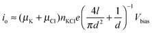 | (1) |
 | ||
| Fig. 1 (left) An α-hemolysin biological nanopore embedded in a lipid bilayer membrane. This protein has been adopted for in vitro nanopore sensing applications due to its ability to permit the passage of small solutes and relatively large macromolecules in a linear conformation such as DNA. Furthermore, α-hemolysin is amenable to protein engineering that can provide single point mutations in the vestibule or the barrel that can later be used in the conjugation of recognition elements. (right) A cross-sectional illustration of a typical solid-state nanopore fabricated in a silicon nitride membrane. The pore diameter can be finely tuned and typically ranges from 2 nm upwards. The nanopore shape can approximate an hourglass, cylinder, or cone, depending on the fabrication methods. In cylindrical nanopores, the depth is defined by the thickness of the membrane and typically takes on dimensions of approximately 10–200 nm. Silicon nitride nanopores are easily amenable to modification by using either surface chemistry or semiconductor processing techniques. | ||
 | ||
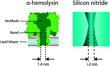
| Fig. 2 (a) The schematic shows the ionic current recorded as a function of time and the interpretation of the analyte translocation process. The steady-state ionic current is decreased when the analyte is translocated through the pore and then re-established when the molecule exits the pore. (b) Four parameters are generally used to characterise the translocation process: (i) The blockade duration or the time the molecule spends in the nanopore (tdwell). (ii) The amplitude of the blockade current (i.e. difference between open-pore current and the blockade current). (iii) The time between translocation events (τ). (iv) The capture rate defined as the number of translocation events per unit time. All parameters are directly dependent on the applied bias, and nanopore geometry as shown in eqn (1) whilst (iii) and (iv) are also dependant on the analyte concentration. | ||
 | ||
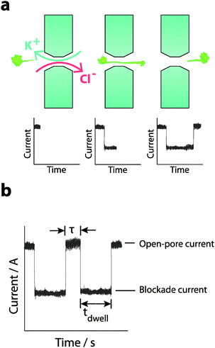
| Fig. 3 Examples of current time traces for 25-bp dsDNA (blue), 22-bp dsRNA (red) and phenylalanine tRNA (black) measured using a 3 nm diameter pore in a 7 nm thick silicon nitride membrane are shown. The concentration for each sample was approximately 80 fmol μl−1. The data shown above nicely demonstrate how analytes with different size and structure result in different blockade amplitudes and blockade times. The mean translocation times for the DNA, RNA and tRNA molecules are 20 μs, 50 μs and 1.04 ms. The histogram clearly shows that these samples can be distinguished in a complex population. Figure adapted from Wanunu et al.1 | ||
Single molecule (bio)sensing with nanopores
In the early 1990s an idea was proposed, see Branton et al.,3 that if a single strand of DNA could be threaded through a nanopore in such a way that discrete conductance blockade levels could be discerned for each of the four bases, it would be possible to sequence the entire strand of DNA. This idea critically altered the perception of what nanopores could do, by introducing the possibility of DNA sequencing. Since then, this novel paradigm has been fuelling the nanopore community to develop ideas and applications not only based around DNA sequencing, but sensing in general. For example, almost two decades ago, Bezrukov and colleagues4 published a seminal work demonstrating that Polyethylene Glycol (PEG) polymers could be translocated and detected through an oligomeric-peptide pore known as alamethicin using ionic-current blockade methods. This was followed shortly after by Kasianowicz et al.5 who published landmark work that demonstrated single stranded DNA (ssDNA) and RNA molecules could also be translocated through an α-hemolysin protein nanopore.Building upon this early work, synthetic nanopores with diameters comparable to biological pores were successfully fabricated in solid-state materials and have been gradually growing in popularity due to their possibility of being integrated with more sophisticated electronics, surface modifications and whole platforms. Over the last decade excellent progress has been made in solid-state nanopore detection: a number of research groups worldwide have actively contributed to the development of nanopore detection from an initial method of detecting single molecules to a powerful technique capable of studying complex molecular interactions and even mimicking biological systems, some of which will be discussed in due course.
Whilst the biological nanopore literature is both vast and impressive, the reader is referred to review articles by Howorka and Siwy,6 Bayley and Martin,7 and most recently by Wanunu8 for a detailed overview of biological nanopore sensors, this tutorial review is focussed on discussing novel methods and materials in the context of solid-state nanopores. Due to the simplicity of the fundamental principles of nanopore sensing, the inherent flexibility of the method and the technology available for chemical modification and fabrication of components around the nanopore, researchers continue to innovate within the bounds of nanopore sensing.
Development of solid state nanopore architectures
The fabrication of solid-state nanopores and membranes can typically be considered as a two-stage process. Firstly, solid-state membranes are fabricated. Secondly, one or multiple nanopores are incorporated into the membrane. In the following sections both of these aspects will be discussed sequentially.Membrane materials
The fabrication of membranes is achieved through industry-standard semiconductor processing techniques that allow for the rapid parallel production of “chips”. Approximately 200 to 500 chips can be produced per 100 mm wafer. A chip consists of a thin free-standing membrane on a support structure. Often the support is made from silicon and the membrane is made from a dielectric material such as low-stress silicon nitride (SiNx). SiNx is mechanically robust, possesses good insulating properties and has been shown to be chemically stable over a range of electrolyte concentrations, pH and temperature. A further advantage is in the ease with which the nanopore surface can be modified either chemically or by incorporating further fabrication steps. Membranes can also be fabricated from other materials such as SiO2,9 SiC,10 Al2O311 or graphene12 if particular chemical or physical properties are desired.Fabrication work-flow of free standing silicon nitride membranes
The simplest workflow of solid-state membrane fabrication consists of the following steps as shown in Fig. 4: (1) A SiNx film is deposited using low-pressure chemical vapour deposition (LPCVD) on both sides of a silicon wafer. (2) Standard photolithographic techniques (spin coating of photoresist, patterning by exposure to UV light, and development of the pattern) are used to define membrane features. (3) Reactive ion etching (RIE) of the SiNx is performed to “open” designated patterns on the bottom side of the wafer. (4) The silicon exposed in these patterns is then removed by anisotropic wet etching using a potassium hydroxide (KOH) aqueous solution. KOH is highly selective to Si13 and the etching of Si results in the formation of free-standing SiNx membranes. It is essential for membrane fabrication, that the deposited SiNx has a low tensile stress and is non-stoichiometric – often referred to as silicon-rich nitride. Stoichiometric silicon nitride films have a high residual tensile stress, exhibit low mechanical stability and chemical resistance, and therefore are poorly suited to membrane fabrication. Often the membrane lateral dimensions range from 7–50 μm, whilst the thickness dimension (l) typically ranges between 10–200 nm. These combined dimensions typically result in aspect ratios between 1![[thin space (1/6-em)]](https://www.rsc.org/images/entities/char_2009.gif) :250 to 1:1000.
:250 to 1:1000.
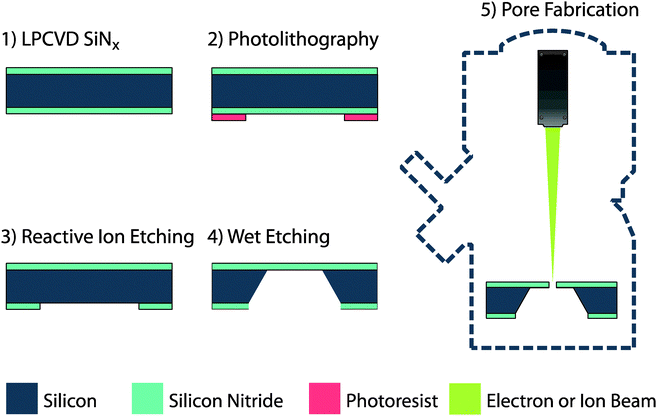 | ||
| Fig. 4 Workflow for the fabrication of a basic membrane and nanopore. | ||
It should be noted that, for the membrane, thinner is usually better, as decreasing the membranes thickness will result in an increase in signal amplitude (the difference between the open pore current and the blockade-current). This can be seen from eqn (1) where thinner membranes (shorter pore length, l) result in a higher open-pore current, io. Unfortunately, the trade-off is that the thinner the membrane, the more fragile it becomes. Nevertheless, sub-10 nm thick membranes have been reported by thinning a small section of the membrane using a combination of lithographic and etching techniques.1 One interesting possibility that has only recently been explored is the use of single or multi-layered graphene as ultra-thin membranes with atomic thickness.
Apart from the membrane thickness, the membrane material, various parasitic capacitance contributions associated with the membrane support and surface chemistry play a significant role in the signal quality observed during a nanopore sensing experiment. In contrast to the membrane thickness, these do not contribute to the signal amplitude obtained from a translocated analyte, however they do add to the noise in a measured signal.14 Due to membrane parasitic capacitances noise increases with the signal bandwidth, making it increasingly more difficult to distinguish meaningful data with high temporal resolution. The signal quality has been shown to improve by coating the membrane surface with polymers.14,15 Alternatively membrane minimisation and the integration of electronics within the membrane has also been shown to improve noise characteristics.14,16,17 This particularly highlights a significant advantage of solid-state membranes where by electronics can easily be integrated into the support structure.
Origins of nanopore fabrication
The final stage of the process when fabricating a nanopore sensor is to incorporate the pore into the membrane. In the last decade, a multitude of techniques have been developed for the fabrication of nanopores in freestanding membranes. Fig. 5 compares typical nanopores fabricated by various techniques that are mentioned below. Whilst key milestones of nanopore fabrication are reported here, focus is particularly given to the current state-of-the-art technologies. There is a great body of work on nanopore fabrication to date, Healy et al. provides a very good review on the subject.18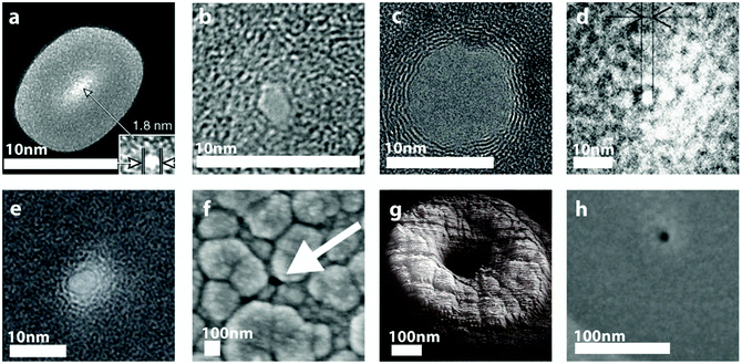 | ||
| Fig. 5 Various SEM, TEM and AFM images of nanopores fabricated in solid-state membranes. (a) A 1.8 nm nanopore in SiNx using Ar-ion beam sculpting19 (inset shows higher magnification TEM image of the nanopore). (b) A nanopore drilled in SiO2 using a tightly focused electron beam with an initial diameter of about 6 nm and reduced to a final diameter of 2 nm after high-intensity wide-field TEM illumination.9 (c) A TEM image of sub-10 nm nanopore fabricated by transmission electron beam ablation lithography in graphene.22 (d) A TEM image of a 3 nm pore milled with a Ga focused ion beam in a 20 nm thick SiC membrane.10 (e) 4 nm nanopore fabricated using a He ion microscope in a SiNx membrane.26 (f) A 100 nm nanopore electrochemically deposited with Pt to produce a final nanopore diameter of approximately 18 nm.30 (g) An AFM image of a 500 nm pore deposited with local oxide deposition with ion-beam induced deposition resulting in a final pore diameter of 30 nm.31 (h) A 50 nm pore deposited with local oxide deposition with electron-beam induced deposition resulting in a final pore diameter of 2 nm.32 All figures obtained with permission. | ||
As a brief overview, the first successful fabrication of nanopores in solid-state materials with single-nanometre resolution was reported in 2001 using a technique coined as ion beam sculpting.19 In this experiment nanopores with diameters as small as 1.8 nm could be achieved. Following the success of ion beam sculpting, a variety of electron beam assisted techniques were developed to “sculpt” or directly fabricate pores with diameters of a few nanometres in solid-state membranes. The first fabrication of nanopores with sub-10 nm diameters using an electron beam were performed by Storm et al.9 who initially combined electron beam lithography (EBL) and anisotropic etching to produce nanoscale pores in SiO2 membranes. Subsequently the pores were thermally oxidised and subjected to a high-intensity wide-field illumination with a transmission electron microscope (TEM) that decreased the pore diameter. This approach yielded solid-state nanopores with single-nanometre precision. Importantly, the experiment performed by Storm et al. also demonstrated that a tightly focused high-intensity TEM beam could be used to directly drill sub-10 nm nanopores in thin membranes. In later studies, direct milling of nanopores with high energy electron beams has been carried out successfully in a number of membrane materials including metal oxides,20 SiNx,21 and graphene.12,22–24
Nanopore fabrication: state-of-the-art
At present, conventional solid-state nanopore fabrication can be achieved by using two possible routes; either by using electron beams as described above or alternatively by milling a pore with a focused ion beam (FIB).Direct milling with focused electron beams is still predominantly used for the fabrication of small nanopores with diameters typically between 1 and 10 nm. At the same time, FIBs are widely popular as they allow for greater flexibility with respect to the dimensions and materials used. In principle any ion with sufficient energy to sputter atoms away from the membrane surface can be used for nanopore fabrication. For example, ion beam sources such as Ga+, He+, Ne+, Ar+, Kr+, and Xe+ have all been reported to successfully be used for milling or sculpting nanopores.25 Ga is arguably the ion source that is most frequently used for nanopore milling, although there is a potential disadvantage associated with ion implantation that can result in modification of the nanopore surface charge. However, Ga+ milling is a well-established technique for milling pores with diameters typically greater than 20 nm, although recently sub-5 nm diameters have also been documented as shown in Fig. 5d.10
Another interesting possibility is the use of a helium ion microscope (HIM) to fabricate nanopores. The HIM uses an ion source with an atomically sized tip that allows for the instrument to produce a highly focused ion beam and to fabricate pores with diameters as low as 4 nm (shown in Fig. 5e).26 The technique has some advantages compared to traditional gallium ion fabrication such as higher resolution, no ion implantation and the possibility of directly thinning sections of the membrane.27
Fine tuning the pore dimensions
Apart from the direct methods for fabricating nanopores, there is a selection of advanced techniques that can augment the traditional fabrication procedures. For example, atomic layer deposition (ALD) can be used to deposit, with sub-nanometre precision, single layers of high dielectric constant materials such as Al2O3.11,20 Al2O3 membrane structures have been reported to exhibit enhanced mechanical properties, and low noise performance compared to SiO2 and SiNx respectively. In addition ALD can enable nanopore integration with novel membrane architectures such as graphene – Al2O3 multilayered nano-laminates28 or lipid bilayer coated Al2O3 hybrid membranes.11Other, easily accessible methods for fine-tuning nanopore dimensions include sputtering and evaporation. Wei et al.29 showed that the deposition of a gold layer with a thin titanium adhesion layer can conform to the nanopore surface and result in a decreased nanopore diameter. This methodology can be extended if electrodeposition is used to further control the pore dimensions as described by Ayub et al., Fig. 5f.30 In these latter experiments, nanopores were milled in gold-coated SiNx membranes and platinum was electrodeposited at the nanopore interface. Importantly, this approach allowed for direct monitoring of the nanopore ionic conductance during the deposition process. This unique feature provides real-time feedback on the rate of deposition and pore dimensions. The techniques used, as described above, coat the entire membrane and as a consequence this results in the entire membrane properties being altered. Recently however, local oxide deposition in the vicinity of the nanopore has been shown to circumvent this limitation. For instance, using a tetraethylortho-silicate (TEOS) precursor or a mixture of TEOS and water vapour, the diameter of relatively large pores milled with FIB were reduced from 500–1000 nm to 25–30 nm with ion-beam induced deposition31 (Fig. 5g) and from 50 nm down to 2 nm with electron beam induced deposition, Fig. 5h.32
In addition to modifying the nanopore geometry, many of the presented methods can be used to further extend the properties of the nanopore and membrane. Examples include controlling the surface charge, fabricating integrated electronics – such as localized electrodes, and incorporating functional groups in and around the nanopore. The latter and the associated fabrication steps are explored in the following section.
Surface modification of solid-state nanopores
The line between nanopore-fabrication and modification is arguably flexible and is indeed a continuum, however in the context of this section any development of the nanopore beyond what can be deemed as the basic and archetypal SiNx nanopore is considered a modification of that nanopore. Furthermore, not all surface modifications need to be ‘chemical modifications’ as they are classically described. Physical modification, that has already been touched on, is particularly useful in the deposition of metals, metal compounds and dielectrics.A great diversity of functions can be appropriated to a solid-state nanopore by chemically modifying the surface. In fact due to the chemical diversity that can be introduced, the primary limit is one's imagination. Several particularly good examples of modification include the immobilisation of single protein receptors via a thiol-terminated self-assembled monolayer (SAM)33 for probing biochemical binding kinetics, immobilization of ssDNA for distinguishing exact target sequences by complementary hybridization34 and nanopores that mimic those found in the antennae of silk moths through the introduction of fluid lipid coatings.35 Within the following section these surface modification methods are discussed in greater detail.
Silane and thiol based modifications
Since SiNx is the most frequently used membrane material, a commonly cited gateway into nanopore modification is by the use of organosilane chemistry. Organosilanes are particularly useful for solid-state nanopores as they form a robust covalent linkage to the nanopore/membrane surface and provide various well-understood functional tail groups. It must be said that technically silane coatings are not considered SAMs, as the formation of the covalent bond between the silane and the surface hydroxyls is not a reversible process and hence not self-assembled such as that of the gold–thiol bond.Silanization of a nanopore is easily achieved through either a vapour deposition or a solution based deposition in a solvent such as toluene or methanol. Organosilanes require exposed surface hydroxyl groups to covalently bind to the substrate. Generally the best approach for obtaining a high surface density of hydroxyl groups is to incubate the nanopore chip in a piranha solution (mixture of H2SO4 and H2O2), which acts as a strong oxidiser. This solution also has the additional benefit of removing organic contaminants and improving nanopore wettability. Silanes come in a variety of flavours typically consisting of three head groups such as ethoxy, methoxy or chloride groups based around a silicon atom, with a single functional moiety at the tail, Fig. 6.36
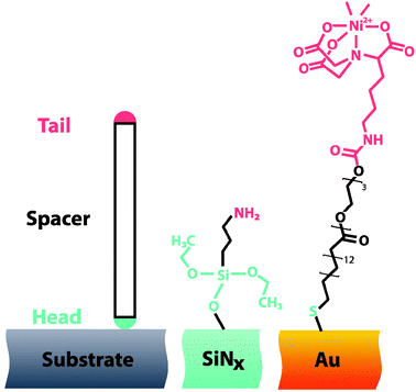 | ||
| Fig. 6 (left) Typical surface modifications are generated using compounds consisting of tail, spacer and head groups. The head group chemisorbs or immobilizes the molecule to the surface and determines the lateral interactions between adjacent molecules. The spacer controls the length and minimizes steric interactions, and can contribute to intermolecular interactions. Finally the tail provides chemical functionality. Two examples of nanopore surface modifications include (middle) (3-aminopropyl)triethoxysilane (APTES)42 and (right) SC15EG3-NTA.33 | ||
Silanization of a silicon surface proceeds by the leaving groups of the organosilane head becoming hydrolysed, then undergoing a condensation reaction with the hydroxyl groups at the nanopore surface. One of the most crucial steps for achieving a robust, high density, silane film is a post silanization bake at ∼100 °C for 16 hours.37 This step crosslinks the organosilane molecules at any unreacted alkoxy groups, though care must be taken to preserve the reactivity of the tail group after baking.
It would be prudent to mention that not all nanopores are amenable to silanization and as a consequence other compounds must be considered. For nanopores that have been fabricated or physically modified with gold, thiol terminated SAMs have proven to be popular38 due to their ease of deposition and versatility in terms of tail groups, see Fig. 6.
Reactive tail groups whether belonging to a functional thiol or an organosilane include amines, epoxides, and sulfhydryls amongst others that each possesses their own interesting properties. These reactive groups can function as a platform for expansion into more complex nanopore modifications as will be shown later.
In terms of rudimentary modifications there is a diverse range of the previously mentioned “tail groups” that can be used to modulate surface charge, respond to environmental conditions or provide steric effects that confer molecular selectivity or alter the nanopore diameter. Wanunu and Meller conducted a substantial exploration of organosilanes and subsequent derivatives working with a SiNx nanopore.39 Surface coatings of amines, epoxides, PEG and carboxyl groups were produced and the coatings were characterized by X-ray photoelectron spectroscopy (XPS). In situ coating was monitored through simultaneous measurement of the ionic-current through the nanopore. Many observations were made however one example is that amine coated nanopores were noted to have a highly pH-dependent ionic conductivity in low salt conditions. Stimuli responsive nanopore modifications that are sensitive to light, pH and temperature are also garnering a fair amount of interest and have been reviewed extensively by Hou et al.40
Biochemical and biomimetic modification
To explore the true nature of bio-molecular phenomena scientists must possess tools that are able to probe the objects of interest at their own scale and relay this nanoscale interaction to the macroscopic world. Biomolecule functionality can be observed through the stochastic sensing of a target analyte by measuring the effect of an immobilised ligand at the nanopore surface on the translocation rate and duration, of the target analyte. Presented here is a selection of the most promising biomolecular and biomimetic nanopore modifications that confer some level of biological function ranging from single protein binding kinetics through to molecular selectivity that mimics that of a mammalian nuclear pore complex.Proteins
In a recent article, Wei et al. demonstrated stochastic sensing with receptor modified solid-state nanopores. This was accomplished by initially modifying the surface with a mixed alkylthiol monolayer on a gold coated SiNx nanopore.33 One dilute component of the mixed monolayer intrinsic to the sensor was triethylene glycol alkylthiol tris-nitrilo acetic acid (NTA). The NTA chelates Ni(II) and this divalent cation was then used to capture poly-histidine tagged proteins shown in Fig. 7a. The binding and unbinding of his-tagged protein A to the Ni(II), and subsequently the binding of antibodies to protein A was observed in real-time. This method was sufficiently sensitive to discriminate different sub-classes of IgG antibodies in a complex mixture.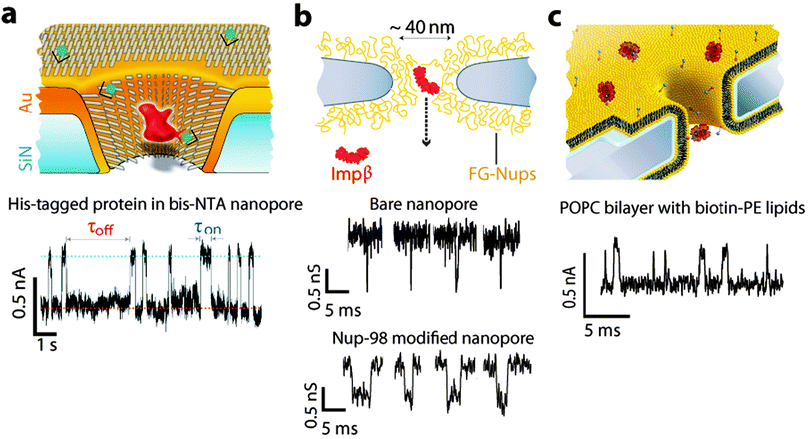 | ||
| Fig. 7 Examples of surface modified nanopore platforms. (a) Schematic of a gold-coated nanopore functionalized with a combination of matrix thiols (SC15EG3) and receptor thiols (NTA). A Ni2+ (green) loaded NTA receptor (black) specifically binds to His6-tagged proteins (red). The blockade time reflects the binding time of the analyte to the receptor (τon). A current time trace is shown for a 26 nm nanopore functionalised with 2 mol% NTA functionalised thiols, and 98 mol% matrix thiols after the addition of 180 nM His6-tagged protein A.33 (b) Schematic of a nanopore functionalised with nucleoporins (FG-Nups). Representative current time traces are shown in the presence of a transport receptor Impβ with and without the FG-Nups modification.42 (c) Conceptual representation of a nanopore functionalised with a lipid bilayer (POPC) containing biotin anchors (blue circles) in the presence of streptavidin (red circles). Example of a current time trace showing the translocation of the biotin–streptavidin complex.35 All figures obtained with permission. | ||
Other examples of nanopore platforms leverage biomimetic design to study complex biological interactions.41 The biomimetic approach has been perfectly exemplified by the following works of Kowalczyk et al.42 and Yusko et al.35 Kowalczyk et al. designed a biomimetic nuclear pore complex, which is selective to the transport of individual proteins. The platform was fabricated by silanizing a SiNx nanopore with 5% (aminopropyl)triethoxysilane (APTES) solution in methanol. This resulted in an amine functionalised nanopore. These amines were then reacted with sulfo-SMCC, a crosslinking agent that contains both a maleimide (sulfhydryl reactive) and an NHS-ester (amine reactive) at opposing ends to achieve a reactive maleimide group at the surface. The SiNx membrane was then incubated with the nucleoporin proteins Nup98 and Nup193. These recombinant proteins were expressed with an N-terminal poly-cysteine repeat to supply sulfhydryl groups to react with the immobilised maleimide for the immobilisation of the nucleoporins as shown in Fig. 7b. The modified nanopore demonstrated a high degree of molecular selectivity for importing the Impβ protein and inhibiting the translocation of non-specific proteins such as bovine serum albumin, much like the biological nuclear pore complex.
Lipids
Demonstrating further the exciting application of biomimetics and inspired by the olfactory sensillia of silk moths, Yusko et al.35 engineered a supported lipid bilayer on the surface of a nanopore by the spreading of liposomes on the SiNx membrane, Fig. 7c. Tailoring the lipid composition yielded control over the nanopore diameter, surface chemistry and the introduction of recognition elements such as biotin. The capture of analytes to the lipid membrane via the recognition element conferred an increased analyte dwell time, aiding detection where 30 to 100 analyte translocations per second were recorded for a 5 pM bulk concentration of streptavidin, Fig. 7c. Fluid lipid bilayer coatings have also been shown for the successful analysis of entities that typically clog nanopores such amyloid-β aggregates.43 Furthermore the use of lipid-bilayer coatings has enabled the fabrication of vast nanopore arrays with well-defined pore geometries.44Nucleic acids
Mussi et al. exploited the familiar and reliable silanization of a SiNx nanopore with APTES and subsequently coupled amine functionalized oligonucleotides to the coating via the amine crosslinker, 1,4-phenylenediisothiocyanate. Relative to a target ssDNA sequence, a background matrix of non-complementary oligonucleotides was used to dilute the surface concentration of complementary probe oligonucleotides. There were two outcomes of the nanopore modification. Firstly, the decrease in nanopore diameter, increasing the signal to noise ratio of the ionic current blockade and secondly, the observation of two distinct dwell-time populations, attributed to ssDNA with and without the target sequence.34Beyond ionic current blockade sensing
Currently the ionic current blockade technique is the most widely implemented and extensively developed method for the detection of translocated analytes. However, a number of promising alternative detection methods based on the technology previously described in this tutorial have recently been demonstrated. As it will be highlighted, the nanopore platform has been successfully combined with embedded electrodes, optical detection, and single molecule force techniques. Primarily the goal of developing these platforms has been focused on improving the detection signal quality, adding new detection channels, controlling the translocation process and implementing strategies for creating large arrays of individually addressable nanopores. An overview of selected interesting and novel nanopore technologies is presented here.Tunnelling detection with integrated electrodes
The integration of tunnelling, nanogap electrodes with nanopores (Fig. 8), is proving to be very promising for high sensitivity and high throughput applications. Tunnelling current is measured when a voltage bias is applied between conducting electrodes separated by a gap of just a few nanometres. The tunnelling current is extremely sensitive to the gap geometry, applied bias and the analyte occupying the electrode gap. If the tunnelling gap were to be positioned inside or at the entrance of a nanopore, tunnelling electron technology would enable an additional channel for the detection and analysis of analytes translocating through the nanopore.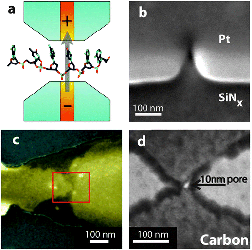 | ||
| Fig. 8 (a) Schematic of a proposed nanopore device with embedded electrodes for tunnelling detection (yellow). The tunnelling electrodes are used to inject a current through the nucleotides in the direction transverse to the DNA backbone. Example images of platforms with integrated tunnelling electrodes include: (b) Electrode gaps, fabricated using electron beam induced deposition, aligned to a nanopore.50 (c) Electrode gaps formed by the electromigration/self-breaking technique on SiO2/Au/SiO2.51 (d) Carbon electrodes aligned to a nanopore.52 All figures obtained with permission. | ||
This technology can offer significant additional advantages over the traditional ionic current blockade detection, such as potentially enhanced spatial resolution, parallel detection with nanopore arrays and the detection of biopolymer composition such as DNA, RNA or even specific peptide sequences. In addition, functionalization of the tunnelling electrodes with recognition elements has been demonstrated to further enhance detection sensitivity and modulate translocation dynamics.45 Perhaps the most compelling application of tunnelling detection, however is, the possibility of achieving fast and inexpensive sequencing of long DNA molecules. The possibility of integrating nanopores with tunnelling electrodes for sequencing DNA was first proposed in 2005 by Zwolak and Di Ventra.46
Nanogap and nanopore requirements
There are a number of considerations for the design of a functional tunnelling gap on a nanopore. The maximum gap distance over which single molecules can be detected by measuring changes in the tunnelling current distribution – depends on a number of factors including: the electrode bias and material, the analyte residence time in the nanogap, the solvent used, and finally, the detection electronics.Under very favourable conditions such as an analyte residence time of a millisecond, a very low input capacitance of a picofarad and a typical bias of 0.5 V applied across the tunnelling electrodes, the maximal gap distance at which a current trace with a sufficient signal to noise ratio to be measured, is estimated to be approximately 4 nm.45 For the tunnelling measurement of submolecular structure, such as the sequence of ssDNA, the gap size must be further decreased to approximately 1.5 nm in order to minimise fluctuations in the tunnelling current due to different molecular orientations in the gap. In addition, to avoid interference from neighbouring bases the electrode width or height has to be comparable to the base spacing in a ssDNA strand (up to ∼0.7 nm for stretched ssDNA).46,47
Electrode fabrication
Initial experiments by Zandbergen et al.48 and later by Fischbein and Drndić49 showed that the methods and materials used in nanopore fabrication (focussed electron beams and solid state membranes) can be feasibly applied to the sculpting of electrodes with sub-nanometre resolution in close proximity or aligned to a nanopore. Later, Gierhart et al. presented the first example of detection with nanogap electrodes integrated on a nanopore. In this work, chromium nanoelectrodes with a nanogap ranging from 2 to 50 nm were fabricated using electron beam lithography and nanopores were fabricated in the electrode gaps by focussed electron beam milling. Nanogap detection was performed using gold nanoparticles and DNA as the analytes.16The first experiments that reported the simultaneous detection of a λ-DNA molecule by ionic current blockade and tunnelling detection were reported by Ivanov et al.50 In this work, electron beam induced deposition was used to fabricate sub-5 nm gaps aligned to a nanopore. At approximately the same time, Tsutsui et al. developed a self-alignment technique to form a nanopore–nanoelectrode architecture capable of achieving a sub-nanometer electrode gaps aligned to a 15 nm SiO2 pore.51 More recently, Spinney et al. adopted an alternative fabrication strategy where a carbon nanowire was sculpted by electron beam assisted etching. A focused electron beam was used to define a nanopore aligned to a pair of tunnelling electrodes. These devices were then used for the detection of λ-DNA and short (16-mer) ssDNA oligonucleotides.52
There are still persistent issues with the successful confinement of individual molecules in the tunnelling gaps during translocation. This can perhaps be addressed in the future with the application of specifically terminated carbon nanotube electrodes53,54 or chemically functionalised nanogaps.45 The fabrication of tunnelling electrodes in close proximity to nanopores has proven to be challenging, however these challenges are being met with perseverance and innovation because the fruits of integrated nanopore electronics are just too great to dismiss.
Optical detection
There are multiple advantages of using optical methods in conjunction with solid-state nanopores. Some of these include high-efficiency optical detection due to confining the analyte in the nanopore, simultaneous ionic current and optical detection and labelling and tracking of different structural or functional segments in a single molecule. Further to the advantages of solid-state nanopores, photonic structures can be patterned near the nanopore surface for enhancing the fluorescence signal in line with fabrication techniques already discussed. Another exciting prospect of using optical detection is the possibility of probing multiple pores simultaneously. This opens the door to facile high-throughput applications.In this section, the advantages of combined optical-nanopore detection are explored in detail. It of course should be noted, that many of the methods required to design and fabricate such platforms, rely on the already discussed techniques covered in Section 2 and 3.
Single molecule fluorescence spectroscopy with metallic nanopores
Fluorescence spectroscopy (FS) is arguably the most widely spread and versatile tool for reliable single molecule detection in solution.55 Hence it is perhaps natural to couple conventional FS with a nanopore architecture. One clear advantage in doing so, is the ability to confine and precisely localise the analyte within the optical detection volume. Furthermore as the nanopore is the only conduit between the two reservoirs it essentially guarantees that every molecule will be detected. This is highly advantageous as in conventional single molecule FS the majority of the analytes bypass the detection volume without being detected.There are various strategies one can use to optically detect translocation events. One option is the incorporation of a metallic layer onto the membrane in order to restrict the propagating light within the vicinity of the nanopore. Membranes coated with metals such as aluminium have been shown to act as an optical barrier (Al is optically opaque in the visible spectrum) between the membrane and the analyte reservoir, Fig. 9.56 When a metallic nanopore is probed with light longer in wavelength than its diameter, an evanescent wave is generated in the nanopore. This mode of detection is very similar to a zero mode waveguide as described by Levene et al.57 and importantly permits the confinement of the optical detection volume to the dimensions of the nanopore. Due to the relationship between wavelength and nanopore diameter the detection volume can easily be tuned by varying the nanopore dimensions.
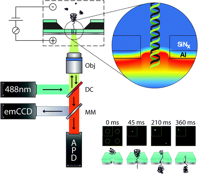 | ||
| Fig. 9 (left) Schematic diagram of the optical setup used for the detection of λ-DNA translocation events. The light from a 488 nm laser excitation source is reflected by a dichroic mirror (DC) situated at 45° and passes through the back aperture of a water immersion 60× objective (Obj). Depending on the optical configuration, this brings the light to a tight focus for single point confocal detection or alternatively wide field illumination can be used to image the entire membrane. Fluorescence from the analyte is then collected through the same Obj and DC. The fluorescence light is either reflected using a moving mirror (MM) on to an emCCD for imaging an array of pores or onto an avalanche photodiode detector (APD) for single point confocal imaging. (top right) False colour image highlighting the evanescent decay of the excitation light within the nanopore and local membrane surroundings. (bottom right) Fluorescence image sequence of two λ-DNA translocation events labelled with YOYO-1. The dotted circles in each frame denote the location of a nanopore. A schematic of the translocation process is also shown for each respective frame. Modified from Chansin et al.58 | ||
A combined optical-nanopore platform exploiting similar principles was reported by Chansin et al.58 In this study, single λ-DNA molecules were translocated through a small array of nanopores with diameters between 200 to 300 nm. The nanopores were fabricated by FIB in a 200 nm thick SiNx membrane coated with a 100 nm Al layer. Under these conditions, high-contrast imaging of single-molecule events was recorded. This work was the first demonstration in the literature of single molecule detection from multiple nanopores in parallel. In addition, it was shown that single nanopores could also be probed using confocal optics with high temporal resolution, enabling more efficient characterization of individual translocation events. The authors conjectured that in time, the system could be optimized to detect signals from hundreds of nanopores simultaneously, creating a truly high-throughput optical detection system that can be used for a wide variety of sensing applications. Such platforms can also be modified with a patterned metallic membrane allowing for the incorporation of plasmonic structures near the nanopore surface. Although this has yet to be demonstrated with a nanopore, one related example by Aouani et al. demonstrated that a 135 nm Au patterned well surrounded by five periodic corrugations resulted in enhanced fluorescence.59
Total internal reflection fluorescence with nanopores
Another promising method for optical detection in nanopore arrays is the use of total internal reflection fluorescence (TIRF) spectroscopy. TIRF is an interesting technique that allows excitation of a very small volume close to the membrane, greatly reducing background fluorescence and enabling single molecule detection. Unlike in the previous examples, a metal layer is no longer needed. In this method, light is introduced “off-axis” relative to the microscope objective and optically coupled into the membrane. This creates a standing evanescent wave of light at the surface of the membrane that extends to about 100 nm into the surrounding medium. Thus, only molecules that enter the evanescent field will be excited and consequently detected. The emitted fluorescence is then recorded using an ultra-sensitive electron multiplying charge-coupled device (emCCD).Soni et al. demonstrated the simultaneous detection of fluorescently labelled 421 bp dsDNA and protein–DNA complexes60 by TIRF and ionic-current blockade in a solid-state nanopore platform. These measurements were performed using a SiNx membrane with a 4 nm nanopore. In subsequent experiments, McNally et al.61 further improved this platform by the introduction of “two-colours” for the detection and characterization of DNA sequences. Firstly, the method biochemically converted a target DNA sequence into an adapted and elongated sequence based upon a 2-bit binary code. Encoded regions on the converted DNA were complementary to fluorescently labelled ssDNA “beacons”. As the converted sequence with hybridized beacons was translocated, the beacons were stripped off and their fluorescence only observed as they were liberated. The fluorescence signals were then analysed based upon the 2-bit, binary encoding to reconstitute the original DNA sequence. Not only did McNally and co-workers demonstrate the optical detection of single molecules using TIRF, but also the detection of discrete optical signals from multiple nanopores proving the utility of the method for high-throughput molecular detection.
Optical readout of large nanopore arrays
One of the inherent advantages offered by using optical detection methods is the ability to interrogate multiple nanopores simultaneously, which cannot be easily achieved when using ionic-current blockade detection, as addressing individual nanopores within an array requires independent electronics and reservoirs for each nanopore. Although headway62 is being made in this context, a much simpler option is to use FS. An interesting application of the latter is the integration of solid-state nanopores and lipid bilayer membranes for high throughput detection. Recently, Kleefen et al. created solvent free suspended lipid bilayers on a solid-state 45 × 45 nanopore array. The nanopores in each array had diameters ranging from 15 to 100 nm. In an unprecedented breakthrough, the platform allowed for the monitoring of up to 1000 translocation events simultaneously.44Another example by Im et al. demonstrated that Au nanopore arrays can be used for surface plasmon resonance (SPR) kinetic binding assays. In this work, pore-spanning lipid membranes were formed over the nanopores and kinetic assays were performed of α-hemolysin incorporation in to the bilayer membrane. The transmembrane protein was incubated with a specific antibody and the binding was detected via red-shifts in the plasmon resonance of the gold nanopore array.63
Force based nanopore sensing
Force based sensing methods, such as optical tweezers,64 magnetic tweezers,65 and atomic force microscopy66 combined with nanopore technology can provide mechanical manipulation of individual molecules within nanopores to a high degree of precision. The common feature of these methods is that the molecule is tethered to a microscopic object or a particle that can be controlled by the application of force from an external apparatus. In principle all force based methods are sensitive to the size of the analyte inside the nanopore and the local charge density. Hence, these methods permit the study of fundamental biomolecular interactions between a translocating analyte and a nanopore, and molecular interactions such as those in protein–DNA complexes.67Another significant advantage of force based sensing is the possibility to precisely control the translocation speed of an analyte. This can provide valuable additional time for detection, which is usually a limiting factor in nanopore sensing. An excellent review on the application of these methods for controlling the molecular transport through nanopores has been written by Keyser.68
Conclusion
From the biological roots of the nanopore, where it continues to play a countless number of roles that living creatures rely upon, to their current mainstream popularity, they capture the imagination of both scientists and the general public. The field of solid-state nanopores in particular is young and exciting. Novel technologies are continuously pushing the limits and boundaries of fabrication methodologies and techniques that were born out of the semiconductor electronics industry. This momentum has been carried forward to state of the art fabrication techniques and newly discovered materials.For deeper exploration of the biological world, the field once again returns to the roots of the nanopore for inspiration in building biomimetic and bioinspired nanopores that behave like nuclear pores or display biomolecular recognition, all enabled by a diverse set of surface chemistries.
The field not only continues to push the solid-state nanopores themselves, but also the methods used to interrogate these nanoscale volumes. Ionic current blockade sensing has proven to be an extremely useful method for interrogating single nanopores. Beyond conventional ionic-current blockade detection, a number of emerging detection methods exhibit some very exciting directions for nanopore interrogation. Tunnelling electrodes have the potential to probe deep within analyte sub-molecular structures whilst optical methods are permitting large-scale interrogation of nanopore arrays. Force based measurements allow for precise positional control of the analyte enabling increased detection sensitivity. The field of solid-state nanopores is scintillating, unwavering in the face of a challenge and driven by innovative technologies and passionate people. The field is accessible and welcoming, there is much left to discover.
Acknowledgements
This work was supported in part by a European Research Council starting grant and a Leverhulme Trust research grant. BNM acknowledges support from BBSRC and GSK for funding. FD would also like to acknowledge the Tr Ministry of Education for funding.Notes and references
- M. Wanunu, T. Dadosh, V. Ray, J. Jin, L. McReynolds and M. Drndić, Nat. Nanotechnol., 2010, 5, 807–814 CrossRef CAS.
- M. Firnkes, D. Pedone, J. Knezevic, M. Döblinger and U. Rant, Nano Lett., 2010, 10, 2162–2167 CrossRef CAS.
- D. Branton, D. W. Deamer, A. Marziali, H. Bayley, S. A. Benner, T. Butler, M. Di Ventra, S. Garaj, A. Hibbs, X. H. Huang, S. B. Jovanovich, P. S. Krstic, S. Lindsay, X. S. S. Ling, C. H. Mastrangelo, A. Meller, J. S. Oliver, Y. V. Pershin, J. M. Ramsey, R. Riehn, G. V. Soni, V. Tabard-Cossa, M. Wanunu, M. Wiggin and J. A. Schloss, Nat. Biotechnol., 2008, 26, 1146–1153 CrossRef CAS.
- S. M. Bezrukov and I. Vodyanoy, Biophys. J., 1993, 64, 16–25 CrossRef CAS.
- J. J. Kasianowicz, E. Brandin, D. Branton and D. W. Deamer, Proc. Natl. Acad. Sci. U. S. A., 1996, 93, 13770–13773 CrossRef CAS.
- S. Howorka and Z. S. Siwy, Chem. Soc. Rev., 2009, 38, 2360–2384 RSC.
- H. Bayley and C. R. Martin, Chem. Rev., 2000, 100, 2575–2594 CrossRef CAS.
- M. Wanunu, Phys. Life Rev., 2012, 9, 125–158 CrossRef.
- A. J. Storm, J. H. Chen, X. S. Ling, H. W. Zandbergen and C. Dekker, Nat. Mater., 2003, 2, 537–540 CrossRef CAS.
- J. Gierak, A. Madouri, A. Biance, E. Bourhis, G. Patriarche, C. Ulysse, D. Lucot, X. Lafosse, L. Auvray, L. Bruchhaus and R. Jede, Microelectron. Eng., 2007, 84, 779–783 CrossRef CAS.
- B. M. Venkatesan, A. B. Shah, J.-M. Zuo and R. Bashir, Adv. Funct. Mater., 2010, 20, 1266–1275 CrossRef CAS.
- M. D. Fischbein and M. Drndić, Appl. Phys. Lett., 2008, 93, 113107–113107 CrossRef.
- K. R. Williams, K. Gupta and M. Wasilik, J. Microelectromech. Syst., 2003, 12, 761–778 CrossRef CAS.
- V. Dimitrov, U. Mirsaidov, D. Wang, T. Sorsch, W. Mansfield, J. Miner, F. Klemens, R. Cirelli, S. Yemenicioglu and G. Timp, Nanotechnology, 2010, 21, 065502 CrossRef CAS.
- V. Tabard-Cossa, D. Trivedi, M. Wiggin, N. N. Jetha and A. Marziali, Nanotechnology, 2007, 18, 305505 CrossRef.
- B. C. Gierhart, D. G. Howitt, S. J. Chen, Z. ZHU, D. E. Kotecki, R. L. Smith and S. D. Collins, Sens. Actuators, B, 2008, 132, 593–600 CrossRef.
- J. K. Rosenstein, M. Wanunu, C. A. Merchant, M. Drndić and K. L. Shepard, Nat. Methods, 2012, 9, 487–492 CrossRef CAS.
- K. Healy, B. Schiedt and A. P. Morrison, Nanomedicine, 2007, 2, 875–897 CrossRef CAS.
- J. Li, D. Stein, C. McMullan, D. Branton, M. J. Aziz and J. A. Golovchenko, Nature, 2001, 412, 166–169 CrossRef CAS.
- P. Chen, T. Mitsui, D. B. Farmer, J. Golovchenko, R. G. Gordon and D. Branton, Nano Lett., 2004, 4, 1333–1337 CrossRef CAS.
- M. J. Kim, M. Wanunu, D. C. Bell and A. Meller, Adv. Mater., 2006, 18, 3149–3153 CrossRef CAS.
- C. A. Merchant, K. Healy, M. Wanunu, V. Ray, N. Peterman, J. Bartel, M. D. Fischbein, K. Venta, Z. Luo, A. T. C. Johnson and M. Drndić, Nano Lett., 2010, 10, 2915–2921 CrossRef CAS.
- S. Garaj, W. Hubbard, A. Reina, J. Kong, D. Branton and J. A. Golovchenko, Nature, 2010, 467, 190–193 CrossRef CAS.
- G. F. Schneider, S. W. Kowalczyk, V. E. Calado, G. Pandraud, H. W. Zandbergen, L. M. K. Vandersypen and C. Dekker, Nano Lett., 2010, 10, 3163–3167 CrossRef CAS.
- Q. Cai, B. Ledden, E. Krueger, J. A. Golovchenko and J. Li, J. Appl. Phys., 2006, 100, 024914 CrossRef.
- J. Yang, D. C. Ferranti, L. A. Stern, C. A. Sanford, J. Huang, Z. Ren, L.-C. Qin and A. R. Hall, Nanotechnology, 2011, 22, 285310 CrossRef.
- M. M. Marshall, J. Yang and A. R. Hall, Scanning, 2012, 34, 101–106 CrossRef CAS.
- B. M. Venkatesan, D. Estrada, S. Banerjee, X. Jin, V. E. Dorgan, M.-H. Bae, N. R. Aluru, E. Pop and R. Bashir, ACS Nano, 2012, 6, 441–450 CrossRef CAS.
- R. Wei, D. Pedone, A. Zürner, M. Döblinger and U. Rant, Small, 2010, 6, 1406–1414 CrossRef CAS.
- M. Ayub, A. Ivanov, J. Hong, P. Kuhn, E. Instuli, J. B. Edel and T. Albrecht, J. Phys.: Condens. Matter, 2010, 22, 454128 CrossRef.
- J. Nilsson, J. R. I. Lee, T. V. Ratto and S. E. Létant, Adv. Mater., 2006, 18, 427–431 CrossRef CAS.
- C. Danelon, C. Santschi, J. Brugger and H. Vogel, Langmuir, 2006, 22, 10711–10715 CrossRef CAS.
- R. Wei, V. Gatterdam, R. Wieneke, R. Tampé and U. Rant, Nat. Nanotechnol., 2012, 7, 257–263 CrossRef CAS.
- V. Mussi, P. Fanzio, L. Repetto, G. Firpo, S. Stigliani, G. P. Tonini and U. Valbusa, Biosens. Bioelectron., 2011, 29, 125–131 CrossRef CAS.
- E. C. Yusko, J. M. Johnson, S. Majd, P. Prangkio, R. C. Rollings, J. Li, J. Yang and M. Mayer, Nat. Nanotechnol., 2011, 6, 253–260 CrossRef CAS.
- P. Jonkheijm, D. Weinrich, H. Schröder, C. Niemeyer and H. Waldmann, Angew. Chem., Int. Ed., 2008, 47, 9618–9647 CrossRef CAS.
- C. M. Halliwell and A. E. G. Cass, Anal. Chem., 2001, 73, 2476–2483 CrossRef CAS.
- C. Vericat, M. E. Vela, G. Benitez, P. Carro and R. C. Salvarezza, Chem. Soc. Rev., 2010, 39, 1805–1834 RSC.
- M. Wanunu and A. Meller, Nano Lett., 2007, 7, 1580–1585 CrossRef CAS.
- X. Hou, W. Guo and L. Jiang, Chem. Soc. Rev., 2011, 40, 2385 RSC.
- S. W. Kowalczyk, T. R. Blosser and C. Dekker, Trends Biotechnol., 2011, 29, 607–614 CrossRef CAS.
- S. W. Kowalczyk, L. Kapinos, T. R. Blosser, T. Magalhães, P. van Nies, R. Y. H. Lim and C. Dekker, Nat. Nanotechnol., 2011, 6, 433–438 CrossRef CAS.
- E. C. Yusko, P. Prangkio, D. Sept, R. C. Rollings, J. Li and M. Mayer, ACS Nano, 2012, 6, 5909–5919 CrossRef CAS.
- A. Kleefen, D. Pedone, C. Grunwald, R. Wei, M. Firnkes, G. Abstreiter, U. Rant and R. Tampé, Nano Lett., 2012, 10, 5080–5087 CrossRef.
- S. Lindsay, J. He, O. Sankey, P. Hapala, P. Jelinek, P. Zhang, S. Chang and S. Huang, Nanotechnology, 2010, 21, 262001 CrossRef.
- M. Zwolak and M. Di Ventra, Nano Lett., 2005, 5, 421–424 CrossRef CAS.
- J. Lagerqvist, M. Zwolak and M. Di Ventra, Biophys. J., 2007, 93, 2384–2390 CrossRef CAS.
- H. W. Zandbergen, R. J. H. A. van Duuren, P. F. A. Alkemade, G. Lientschnig, O. Vasquez, C. Dekker and F. D. Tichelaar, Nano Lett., 2005, 5, 549–553 CrossRef CAS.
- M. D. Fischbein and M. Drndić, Nano Lett., 2007, 7, 1329–1337 CrossRef CAS.
- A. P. Ivanov, E. Instuli, C. M. McGilvery, G. S. Baldwin, D. W. McComb, T. Albrecht and J. B. Edel, Nano Lett., 2011, 11, 279–285 CrossRef CAS.
- M. Tsutsui, S. Rahong, Y. Iizumi, T. Okazaki, M. Taniguchi and T. Kawai, Surf. Sci. Rep., 2011, 1, 1–6 Search PubMed.
- P. S. Spinney, S. D. Collins, D. G. Howitt and R. L. Smith, Nanotechnology, 2012, 23, 135501 CrossRef.
- E. S. Sadki, S. Garaj, D. Vlassarev, J. A. Golovchenko and D. Branton, J. Vac. Sci. Technol., B, 2011, 29, 053001 Search PubMed.
- Z. Jiang, M. Mihovilovic, J. Chan and D. Stein, J. Phys.: Condens. Matter, 2010, 22, 454114 CrossRef.
- S. Weiss, Science, 1999, 283, 1676–1683 CrossRef CAS.
- J. Hong, Y. Lee, G. A. T. Chansin, J. B. Edel and A. J. de Mello, Nanotechnology, 2008, 19, 165205 CrossRef.
- M. J. Levene, J. Korlach, S. W. Turner, M. Foquet, H. G. Craighead and W. W. Webb, Science, 2003, 299, 682–686 CrossRef CAS.
- G. A. T. Chansin, R. Mulero, J. Hong, M. J. Kim, A. J. deMello and J. B. Edel, Nano Lett., 2007, 7, 2901–2906 CrossRef CAS.
- H. Aouani, O. Mahboub, N. Bonod, E. Devaux, E. Popov, H. Rigneault, T. W. Ebbesen and J. Wenger, Nano Lett., 2012, 11, 637–644 CrossRef.
- G. V. Soni, A. Singer, Z. Yu, Y. Sun, B. McNally and A. Meller, Rev. Sci. Instrum., 2010, 81, 014301 CrossRef.
- B. McNally, A. Singer, Z. Yu, Y. Sun, Z. Weng and A. Meller, Nano Lett., 2010, 10, 2237–2244 CrossRef CAS.
- G. Baaken, N. Ankri, A.-K. Schuler, J. Ruehe and J. C. Behrends, ACS Nano, 2011, 5, 8080–8088 CrossRef CAS.
- H. Im, N. J. Wittenberg, A. Lesuffleur, N. C. Lindquist and S.-H. Oh, Chem. Sci., 2010, 1, 688–696 RSC.
- U. F. Keyser, B. N. Koeleman, S. van Dorp, D. Krapf, R. M. M. Smeets, S. G. Lemay, N. H. Dekker and C. Dekker, Nat. Phys., 2006, 2, 473–477 CrossRef CAS.
- H. Peng and X. S. Ling, Nanotechnology, 2009, 20, 185101 CrossRef.
- G. M. King and J. A. Golovchenko, Phys. Rev. Lett., 2005, 95, 216103 CrossRef CAS.
- M. van den Hout, I. D. Vilfan, S. Hage and N. H. Dekker, Nano Lett., 2010, 10, 701–707 CrossRef CAS.
- U. F. Keyser, J. R. Soc. Interface, 2011, 8, 1369–1378 CrossRef CAS.
Footnote |
| † These authors contributed equally. |
| This journal is © The Royal Society of Chemistry 2013 |