Scalable synthesis and device integration of self-registered one-dimensional zinc oxide nanostructures and related materials
Babak
Nikoobakht
*a,
Xudong
Wang
*b,
Andrew
Herzing
a and
Jian
Shi
b
aSurface and Microanalysis Science Division, 100 Bureau Dr Stop 8372, National Institute of Standards and Technology, Gaithersburg, MD, USA 20899. E-mail: babakn@nist.gov; Fax: +1 30 1926 6689; Tel: +1 30 19753230
bMaterials Science and Engineering Department, University of Wisconsin-Madison, Madison, WI, USA 53706. E-mail: xudong@engr.wisc.edu; Fax: +1 608 262 8353; Tel: +1 608 890 2667
First published on 28th September 2012
Abstract
On integrating one-dimensional (1D) nanocrystals (nanowires) to useful devices, in this review article, we provide a background on vapor-based growth processes and how they impact device integration strategies. Successful integration of nanowires to devices and their scalability simply rely on where and how nanowires are formed, how they are interfaced to other device components and how they function. In this direction, we will provide a discussion on developed growth strategies for lateral and standing growth of semiconductor nanostructures and assess their success in addressing current challenges of nanotechnology such as mass integration of nanowires, and the necessary accuracy in their positioning and alignment. In this regard, we highlight some of our recent work on formation of two-dimensional (2D)- and three-dimensional (3D)- nanowire and nanowall arrays and provide an overview of their structural and electro-optical properties. This will be followed by discussing potential applications of such hierarchical assemblies in light generation, photocatalysis and conversion of motion to electricity.
 Babak Nikoobakht | Babak Nikoobakht is a physical chemist at the Material Measurement Laboratory of the National Institute of Standards and Technology in Gaithersburg, MD. He also holds an adjunct faculty position at the chemistry and biochemistry department of University of Maryland-College Park. He received his PhD from Georgia Institute of Technology in 2002. His research interests include anisotropic growth of nanocrystals and exploring relation between structure, property and function of ensemble of one-dimensional nanocrystals. |
 Xudong Wang | Dr Xudong Wang is an assistant professor in the department of Materials Science and Engineering at University of Wisconsin – Madison. He received his PhD degree from Georgia Tech in 2005. His current research interests include studying the growth and assembly of oxide nanostructures for mechanical and solar energy harvesting, and understanding the coupling effect of semiconductor properties and piezoelectric polarization. |
 Andrew Herzing | Andrew Herzing received his PhD in Materials Science from Lehigh University in 2007 under the supervision of Prof. Christopher Kiely. He was subsequently awarded a National Research Council postdoctoral fellowship to study the nano- and atomic-scale characterization of materials using transmission electron microscopy and microanalysis techniques at the National Institute of Standards and Technology (NIST) in Gaithersburg, MD. Currently a staff scientist in NIST's Material Measurement Laboratory, he is developing techniques to enable the structural and chemical analysis of nanomaterials at ultrahigh spatial resolution. |
 Jian Shi | Jian Shi obtained his BS degree in Materials Science and Engineering at Xi'an Jiaotong University in 2006, MS Degree in Mechanical Engineering at the University of Missouri-Columbia in 2008, and is currently finishing his PhD degree under the supervision of Prof. Xudong Wang in Materials Science Program at the University of Wisconsin-Madison. His research focuses on the nucleation and growth of oxide nanomaterials, photovoltaics, photoelectrochemical cells, nanogenerators and piezotronics. |
1. Introduction
Optical lithography continues to be the most prevalent technique for further miniaturization of electronic circuitry and its components. However, as device miniaturization continues, both complexity of pattern generation and its cost increase,1 limiting the use of such techniques to high-end applications, such as microprocessor manufacturing. As an alternative, nanomaterials and non-conventional nanofabrication methods such as “bottom-up” chemical approaches could offer platforms to fill the technological gaps with potential advantages in terms of performance and/or cost.Foreseen for many applications, the expected function of a nanostructure in a given device is not the only specification on the quality assurance check list. There are other requirements including structural and performance reliabilities that must be understood and modeled in order for the nanodevice to be considered industrially and commercially viable. In this regard, mass interfacing of semiconductor nanostructures with other semiconductors or metals remains among the technical barriers that must be addressed for realization of platforms that enable control over circuit topology and devices therein. Furthermore, chemical, physical and structural properties of these junctions as well as the device functions must be predictable.
In this review article, we provide readers an account on the progress, challenges and underlying problems in developing useful architectures for nanodevice fabrication via vapor deposition techniques. This overview also provides examples on popular semiconductor oxides such as ZnO and TiO2 and discusses important elements needed in the process of materials design to device innovation, though, the underlying emphasis remains on the directed assembly and interfacing of 1D-nanostructures. This is an important topic, which has to be addressed in any nanowire device integration regardless of the nanowire growth method. The evaluation of candidate materials, their applications and the critical issues related to producing practical devices, both in planar and free-standing formats will be discussed as well.
2. Significance of 1D-semiconductors and the need for alignment techniques
1D-nanostructures share some common characteristics with their 0D- and 2D- counterparts, such as quantum size effects, but geometrically offer advantages that are absent or difficult to realize using the other two categories.2 By definition, nanowires offer a unique combination of dimensionality, where the longitudinal direction exceeds hundreds of nanometers or even micrometers in length while the transverse direction is confined to a few tens of nanometers or less. Since the former is accessible using current microfabrication techniques, the topographies and architectures of nanowire-based devices offer the potential for probing materials at the sub-100 nm dimension.In addition, due to their larger surface area, they are more susceptible in sensing the variation in their immediate surroundings. This has led to realization of novel platforms, for instance, in biosensing.3 2D-film growth typically requires cumbersome growth chambers while high quality nanowires can be formed using inexpensive vapor phase transport or solution-based methods. As discussed in the following sections, nanowires offer the ability to form unconventional crystals, e.g., by extending their anisotropic growth to a 3D network such as hyperbranched nanowires. Using such nanosystems, it is also possible to realize crystal facets that are not thermodynamically observable in thin films; for instance, the formation of non-polar facets in wurtzite crystals important in light emitting devices. Other benefits exhibited by nanowires, compared to a 2D film, could include more degrees of freedom in managing their defects, lattice constant, lattice strain, and doping profile. Owing to their small volume and interfacial areas, the above properties are expected to result in novel material combinations and device concepts.
Some of the earliest reports on the growth of nanowires or whiskers dates back to the 1960s4,5 and 1970s.6–8 However, research on 1D-nanostructures was limited until the late 1990s boom of research on this topic,9–11 perhaps due to the rise in demand for alternative nanosystems to silicon microelectronics. Nowadays, research on nanowires has deeply penetrated various disciplines including chemistry, materials science, physics, biology and engineering with emerging applications in clean energy, sensors, catalysis, electronics and digital displays.
One of the fundamental challenges in integrating free-standing semiconductor nanowires with the highly ordered components of an electro-optical or electro-mechanical device is being able to control the overall hierarchy of nanowires either in planar or standing format.12–14 Another issue is how to accurately position the active area of the individual nanowires between the necessary electrodes within a device. An ideal method for controlling these parameters should enable the reproducible placement of nanowires on a large scale such that their position and orientation are predictable. In recent years, several methods have been devised for incorporating free-standing nanowires into planar devices. The common feature in these methods is the need for a substrate to receive the nanowires and an external force to drive the transfer and alignment of nanowires onto this substrate. A variety of driving forces such as capillary forces,15,16 shear stress,17 adhesion forces,18–20 inertial forces21 and nanopatterning18,22 have been utilized to control the orientation of an ensemble of nanowires on a given surface. Among them, nanoimprint lithography and pattern transfer techniques23,24 demonstrate the most promise in terms of precision and control. However, their use becomes challenging and costly as the relevant object sizes drop below 100 nm or as nanoobject number per site is reduced. Overall, current technologies are more suited to the collective integration of monolayers of nanowires with devices; for instance, in flexible electronics,25 transistors,13 and sensory applications.12 For applications that require electrically addressing single or small groups of nanowires in a scalable fashion, the inherent uncertainties of the available techniques make them incapable of competing with top-down strategies for the realization of complex architectures and circuitries.
3. Growth mechanisms of nanowires and challenges in scalable interfacing
In general the synthesis of nanowires can be classified into two groups of growth processes: metal-catalyzed, and metal-free7 that can take place in solution and in the gas phase. In the first group, also known as vapour–liquid–solid (VLS), vapor–solid–solid (VSS) and solution–liquid–solid (SLS) growth techniques, a metal catalyst acting as a nanoscale solution, dissolves the incoming semiconductor precursors from the gaseous (or solution) phase and confines the nanocrystal growth, resulting in the formation of free-standing nanowires. Such nanowires can typically be distinguished from those produced via other growth processes by the observation of a solidified droplet at their tip. In contrast, metal-free nanowire growth is generally considered to be a vapor–solid (VS) or solution–solid (SS) growth process. Among the factors that are known to initiate this type of growth are surface defects in the substrate such as impurities or screw-type dislocations.7,26 In addition, imbalances in the stoichiometric ratio of the precursors during crystal growth could also result in precipitation of an excess component on some crystal facets, thus stimulating the VS or SS growth.27 In solution phase, nanowires are generally grown in colloidal form28,29 or on a solid surface.30,31 In this case, analogues to the VS growth, nucleation sites are typically necessary to initiate the growth. Examples include growth of ZnO or TiO2 nanowires in which a seed layer is first deposited on the surface of interest to start the growth. Similar to gas phase techniques, this method is also shown to be capable of forming well-aligned and high quality free-standing nanowires32–34 with applications in hydrogen generation,35 dye-sensitized solar cells,36 and energy generation.37Site selectivity of the growth in both gas phase and solution phase methods have been controlled using natural surface defects such as screw dislocations of the underlying substrate26 or using surface patterning techniques. Although the first approach is inherently scalable, its main drawback is the lack of site specificity. The surface patterning can predictably control the position of the nanowires and has been shown on small scales via high resolution patterning,38 and on larger scales using interference photolithography.39 Masking a surface with 1D nanopatterns has also been used for horizontal growth of nanowires in which they are either grown nearly parallel to the surface, but in a suspended form,37 or grown laterally in full-contact with the substrate.22 In the latter group of approaches, the width of the opening in the mask determines the nanowire width. As such, to grow small diameter nanostructures, it becomes necessary to use high resolution lithography for nanopattern generation.22
ZnO and TiO2 are the two most intensively studied semiconductor oxide materials and many of their methods of synthesis have been successfully applied for 1D-growth of other nanostructures such as SnO2 (catalytic VLS, Molecular Beam Epitaxy, Pulsed Laser Deposition),40–43 V2O5 (thermal evaporation, hydrothermal, sol–gel and electrodeposition),44–47 WO3 (CVD, hydrothermal, electrodeposition),48–50 and Fe2O3 (CVD, flame synthesis).51–53 As it can be seen, nanowire growth strategies including VLS, SLS, VS or SS are well-developed and offer unique capabilities such as simplicity, scalability, site specificity, control over composition and control over morphology. These methods can be utilized separately or combined to prepare nanostructures with unprecedented form factors such as homo- and heterojunctions, tubular quantum wells, and shells with axial or radial configurations.54–62 Diversity in device shape is one of the unique distinctions of 1D-nanocrystals that cannot be achieved in 2D-films due to geometrical constrains.
In interfacing nanowires, it is the nature of an application or a device function that determines the method of integration and the necessary hierarchy of nanowires in a device. For instance, if a 2D-network of nanowires is needed to form an electrically conductive layer, then control over the registration of the nanowires may not be as important as their electrical connectivity within the network. However, if the application requires charge transport through a single nanowire or a particular group of nanowires, without intercepting each other, then control over their relative position and orientation becomes crucial. One of the existing challenges is that most of the methods highlighted above yield randomly distributed nanowire networks which their interfacing to outside world is a daunting task. One quick fix to this limitation has been the use of bulk of nanowires in randomly distributed nanowire networks, however, this arrangement typically do not exhibit the performance of original nanowires.
In addition to the use of alignment techniques discussed in Section 2 for building 2D- or 3D-nanoarchitectures, intrinsic structural relationship between a substrate and nanowires can be used to control their overall hierarchy. These approaches naturally enable control of the organization of nanostructures on a wafer scale, leading to more facile device integration. One of the requirements of this methodology is the ability to predictably guide the growth of 1D-nanostructure from a specific site and facet. In the following sections the focus is given to the mutual interactions between substrate and nanowires and factors that guide the nanocrystal growth on or from a single crystal substrate. Well known examples of these processes are free-standing and lateral growth of semiconductor nanowires, which are discussed in the following sections.
3.1 In-plane and out-of plane directed growth of nanowires
The anisotropy of a crystal, in general, is a result of the varying growth kinetics of different crystal faces. One of the fundamental needs in anisotropic crystal growth is the development of methods to selectively grow a nanocrystal facet in a certain direction. Free-standing nanowires are great examples of this as growth occurs only along a selective facet, and thus in a specific crystallographic direction. The particular direction in which a given nanowire will grow is strongly influenced by the crystal structure of the nanowire itself, as well as by the surface free-energy of the metal and semiconductor interface. For example, nanowires with cubic structures typically grow in the 〈111〉 direction, while those with wurtzite-type crystal structure tend to grow in the 〈001〉 direction.63 The substrate is also considered one of the factors determining the growth direction of free-standing nanowires. In the case of lattice matched epitaxies, they can be chosen to guide the growth in a direction which is either normal to or inclined with respect to the surface; for instance, the growth of Si nanowires on a Si (001) substrate, which takes place in the 〈111〉 direction.11 Even in lattice mismatched systems, it has been shown that the substrate impacts the growth direction of the nanowires. Examples include the preference for epitaxial and upright growth of InAs and InP nanowires to occur in the 〈111〉 directions on a Si (111) surface. As the diameter of such nanowires increases, population of the tilted nanowires increases, most likely to reduce the misfit strain between the two crystals.64 In these examples, the growth is no longer epitaxial above a critical diameter due to the increase in strain energy at the interface and the formation of misfit dislocations.65In addition to the role played by the substrate, the interfacial energy and surface tension from the edge of the interface between the metal catalyst and a nanowire are found to be important factors in determining the growth direction of nanowires. In the case of Si nanowires, as the diameter increases the plane of growth changes in order to lower the interface energies between metal catalyst and the semiconductor.66,67 For instance, the growth direction of a population of nanowires has been shown to change from the 〈111〉 to the 〈110〉 direction as their diameter increases above 20 nm.68 Other factors affecting the diversity in nanowire growth directions include the growth temperature, concentration of precursors in the gas phase11 and degree of the supersaturation inside the metal catalyst.63 Although the origin of the multiplicity of nanowire growth direction is fairly well understood, factors that can selectively initiate or abort growth of a specific facet remain elusive. In this regard, we will discuss how the inherent information present on the surface of a single crystal substrate has been utilized as a scaffold to promote growth of 1D- and 2D-epilayers of other materials. This is followed by a discussion on weaknesses and strengths of available approaches in planar growth of nanowires with higher precision and predictability.
Reports on the planar or lateral growth of 1D-nanostructures have been very limited relative to those focused on free standing nanowires. The planar growth can be linked to the original work on the self-assembled epitaxial growth of quantum dots, where epitaxially grown films undergo a transformation to arrays of 3D islands.69 The island formation is typically accompanied by generation of misfit dislocations depending on the extent of lattice mismatch. In the case of Ge on Si (≈4% lattice mismatch), Eaglesham and Cerullo discovered dislocation-free island formation at the expense of elastic deformation of the surrounding substrate. As the islands are overgrown above a critical thickness, misfit dislocations appear as a stress-relief mechanism.70 If the stress is anisotropic, as in the case of Ge on Si, the island aligns itself perpendicularly to the direction of maximum stress. As the lattice mismatch increases, the anisotropy in the island shape becomes more pronounced. Anisotropy in crystal lattice match on a cubic substrate, such as silicon, has been used to transform thin films of rare earth silicides into metal silicide nanowires under a thermal annealing process. As a result of this heat treatment metal silicide nanowires are formed that are approximately 1 μm in length and 2 nm in height.71 Such growth methods typically require dissociation and reconstruction of surface deposited atoms on the heated silicon surface in order to drive the formation of nanowires or quantum wires. In these cases, as the lattice mismatch along the width of the nanowires increases, both the width and height of the nanowires tends to decrease.72 The width distribution of such nanowires is very broad indicating that their formation takes place far from equilibrium. In most of these cases, nanowires tend to grow from both ends and nucleate in closely-spaced groups, with no control over their location or orientation.
Lateral growth of nanowires is also shown to be driven by anisotropy in surface energy73 and symmetry breakdown of the underlying substrate.74 In the latter approach, also called “endotaxial” growth, transition metals are deposited on a Si surface at elevated temperatures. The epitaxial growth of nanowires continues into the substrate such that two of their long facets become embedded in the underlying silicon. The anisotropy driving the nanowire shape has been attributed to the varying growth rates of the nanowire end facets versus its embedded side facets. This synthetic route is applicable to a variety of transition metals, but lacks the necessary control of the overall nanowire morphology. Lower temperatures have been used to increase the aspect ratio of the resulting nanowires, but this also increases the nucleation sites, i.e., their surface density, which decreases their spacing.75
Self-organization of 1D-nanostructures has been also shown using surface defects or structures on a single crystal surface. These approaches can be considered part of the graphoepitaxy methodologies (a.k.a artificial epitaxy) in which artificial micropatterns on a surface are used for growth of oriented crystals. Developed in the early 1970s, this approach was originally proposed for epitaxial thin film growth on amorphous surfaces.76 The created surface patterns must have a symmetry analogous to that of the material to be crystallized on the surface.76 For anisotropic nanostructure growth, single crystal surfaces decorated with surface reconstructions or atomic steps have been used in order to control the directionality or alignment of the grown 1D-nanostructures. Examples include the use of arrays of Al atom of a-plane sapphire,77 atomic steps78 for the alignment of single-walled carbon nanotubes, or the growth of Ge nanowires on step defects on a silicon (113) substrate.79 These approaches offer low-level control of orientation of the resulting nanowires in the formed hierarchy. However, they do not allow for any control over the reproducibility of the surface nanopatterns. The use of arrangement of atoms on a crystal surface potentially is one of the ultimate mechanisms to precisely guide 1D-planar growth; however, the homogeneity of substrate surface energy causes the overgrown islands to lack site-specificity and thus grow randomly. To break this surface degeneracy, metal nanodroplets used in the VLS growth process are found to be very unique, as they precisely define the nucleation sites and confine the nanocrystals growth.
3.2 Surface-directed growth of nanowires
The surface-directed vapour–liquid–solid (SVLS) growth process is nearly identical to the VLS growth of standing nanowires. In the latter, a metal nanodroplet as a solution captures the incoming precursors from the gas phase, reaches a state of supersaturation, and allows precipitation of a semiconductor nanocrystal on the substrate. The metal nanodroplet positioned atop the formed resulting nanocrystal gradually grows upward.5,7 In the SVLS process, the metal nanodroplet partially wets the semiconductor nanocrystal and also forms an interface with the substrate. Continuation of this process results in the lateral growth of a semiconductor nanocrystal in a specific direction with the metal nanodroplet at the leading end of the nanowire.80,81The SVLS growth of nanowires was first observed for ZnO when the spacing between Au catalyst particles was increased to distances several times larger than their size (≤20 nm).82 Later, this growth was shown to occur for Au nanodroplets formed at the perimeter of any 2D Au pattern (Fig. 1a). The tendency of the side nanodroplets to form horizontal nanowires is believed to originate from their high mobility at growth temperature of ≈900 °C and their volume increase due to the incoming flux of Zn and O precursors. These factors increase the likelihood of coalescence of the interior Au nanodroplets with the neighbouring ones leading to the formation of free standing nanowires.3,7 As a consequence of this natural selection, the Au nanodroplets at the periphery of the pattern have the opportunity to move laterally on the substrate, catalysing the growth of horizontal nanowires (Fig. 1b). Therefore, for a deposited metal pattern with a given width, both standing and horizontal nanowires are formed.
 | ||
| Fig. 1 Lateral growth of horizontal nanowires from Au catalyst at 900 °C in a tube furnace. (a) Part of a 10 nm-thick Au pattern annealed at 700 °C shows the arrangement of the metal nanodroplets prior to growth process. (b) Oblique view of horizontally grown ZnO nanowires from an Au pattern. After the growth, Au nanodroplets at the center form free – standing nanowires and those at the edges of the pattern result in horizontal nanowires. | ||
A variety of metal catalysts including Au,5 Ag,83 Ni,84 Cu,85 Sn,86 and Fe84 have been used for growth of nanowires using the VLS and VS processes.87 Depending on the application, the proper selection of the metal catalyst is crucial, as it significantly impacts the electronic structure of the nanowires as well as their morphology.83 In the case of ZnO nanowires, it is shown that the use of iron catalyst results in a faster growth rate, but it also induces more oxygen vacancies. Our results also indicate that the Au catalyst is found to be a superior choice compared to Ag and Cu, because Ag tends to evaporate during the high temperature growth and Cu could result in the formation of deep-level impurities.88 However, in the VLS growth of Si nanowires, a reverse trend has been observed, i.e., Au is found to result in formation of deep-level impurities, and Cu metal shows a less deteriorating effect on the resulting optical properties of nanowires.89
In addition to ZnO, in recent years, the SVLS growth has been demonstrated for other II–VI and III–V semiconductors. Examples include the growth of GaAs,81 GaN,90,91 In2O392 and Mg2SiO493 nanowires on substrates such as GaAs, GaN, sapphire and silicon. To better illustrate the directed growth process, consider sapphire, a trigonal/rhombohedral crystal in the hexagonal crystal family with unit cell dimensions of a = b = 0.4795 nm and c = 1.3099 nm. As illustrated in Fig. 2, this crystal has an elongated unit cell along its c axis. When zinc oxide, a hexagonal crystal with unit cell dimensions of a = b = 0.3249 nm and c = 0.5205 nm, is grown on sapphire, horizontal growth is only observed on certain facets such as the a-plane.82 Interestingly, the long dimension of the sapphire unit cell (1.3099 nm) is almost 4 times the ZnO “a” dimension (0.3249 nm), demonstrating a pseudo-lattice match of about 0.8%. This relationship has been accounted for the aligned growth of ZnO in the case of free standing nanowires and uniaxial epitaxy of ZnO films on a-sapphire.94,95
![Hexagonal crystal structure of sapphire and orientation of its a-plane with respect to the [0001] direction. Horizontal ZnO nanowires grow on the a-plane in the [11̄00] direction.](/image/article/2013/CS/c2cs35164a/c2cs35164a-f2.gif) | ||
Fig. 2 Hexagonal crystal structure of sapphire and orientation of its a-plane with respect to the [0001] direction. Horizontal ZnO nanowires grow on the a-plane in the [1![[1 with combining macron]](https://www.rsc.org/images/entities/char_0031_0304.gif) 00] direction. 00] direction. | ||
The horizontal growth of ZnO nanowires takes place in [100] direction, which is also parallel to the [100] direction of the sapphire crystal (Fig. 2). This direction is strictly observed in the majority of the performed growth trials. However, results indicate that the number of growth directions can change at least within the confines of the crystal symmetry of the substrate. As an example, if ZnO nanowires are grown on a GaN substrate, the growth occurs in multiple directions with a 6-fold symmetry (Fig. 3a).96 In this case, the lattice mismatch between ZnO and GaN, in their [100], is only ≈1.8%, in contrast to the 32%-lattice mismatch between ZnO and sapphire; thus the nanocrystal growth is less restricted on GaN. Replacing GaN substrate with (100) silicon results in laterally grown nanowires, but with no clear directionality preference as seen in Fig. 3b. The lack of directionality could be attributed to multiple factors including: (1) existence of the native silicon oxide layer between Si and ZnO during the growth process; (2) 3% lattice mismatch between ZnO (a = 0.3249 nm) and Si (a = b = c = 0.5381 nm); (3) difference in crystal symmetries, i.e., cubic crystal symmetry of Si versus hexagonal crystal symmetry of ZnO. In growth of horizontal Mg2SiO4 nanowires on silicon, a 1 nm thin amorphous layer is observed at the interface, but it does not obstruct the influence of the substrate on the growth direction and despite ≈5% lattice mismatch the epitaxial growth continues following the symmetries of both cubic crystals.93 The influence of the substrate symmetry and epitaxial growth can be overridden by using artificial surface steps and grooves. In this regard it is shown that the fabricated nanosteps on a c-plane sapphire can force the GaN nanowires to grow along the steps and not those directions predicted by the hexagonal symmetries of both crystals.91 Another example highlighting the significance of this relationship can be understood from Fig. 4. This figure shows TiO2 nanowires grown on a GaN substrate that has been patterned with 10 nm-thick Au features. These nanowires are carbothermally grown from TiO2 powder (anatase phase) and as shown in Fig. 4a, demonstrate a growth direction similar to that of ZnO on GaN, i.e., [100] direction. Based on the selected area electron diffraction (SAED) patterns in Fig. 4b, the atomic packing in the TiO2 has a hexagonal structure (ABAB); however, there is a 30° crystal rotation in the TiO2 diffraction spots (highlighted with arrows), which is not observed in the ED pattern of ZnO nanowires in Fig. 4c.97
 | ||
| Fig. 3 Impact of the substrate on directionality of horizontally grown nanowires. (a) ZnO nanowires grown on (0001) GaN illustrate multiple growth directions with a 6-fold symmetry; while on a (001) silicon substrate (b) nanowires show no clear directionality. | ||
![(a) Horizontal TiO2 nanowires grown from Au patterns on (0001) GaN. The highlighted crystallographic axes coincide with two growth directions. (b) SAED pattern of TiO2 nanowires on GaN. (c) SAED pattern of ZnO nanowires on GaN. Both patterns are collected at the [0001] zone axis. The diffraction spots shown with arrows in (b) indicate a 30° rotation in the crystal orientation for TiO2 with respect to ZnO.](/image/article/2013/CS/c2cs35164a/c2cs35164a-f4.gif) | ||
| Fig. 4 (a) Horizontal TiO2 nanowires grown from Au patterns on (0001) GaN. The highlighted crystallographic axes coincide with two growth directions. (b) SAED pattern of TiO2 nanowires on GaN. (c) SAED pattern of ZnO nanowires on GaN. Both patterns are collected at the [0001] zone axis. The diffraction spots shown with arrows in (b) indicate a 30° rotation in the crystal orientation for TiO2 with respect to ZnO. | ||
The directed planar growth of nanocrystals, based on the available models for anisotropic nanocrystal growth, can be explained by the existence of an asymmetric lattice match between the epilayer and the host substrate.71 Based on this model, the observed nanowire growth directions in the SVLS process could be indicative of the presence of high lattice match pathways between the two crystals. However, the presence of these preferred directions cannot be supported by the aforementioned examples as they include highly matched (1.8% mismatch in ZnO and GaN) and highly mismatched crystals (75% mismatch in c-plane ZnO on a-plane sapphire). As such, the results indicate a loose dependence between crystal lattice match and the directionality of the lateral growth. On the other hand, the crystal symmetry of the two crystals seems to be more influential in defining the number of growth directions.
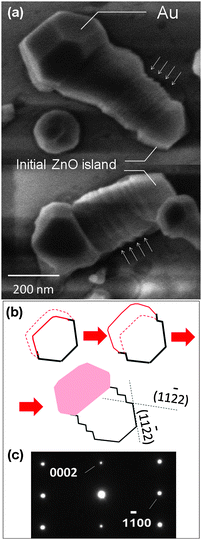
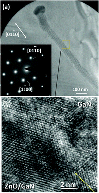
Examination of the interface between ZnO nanowires and the sapphire substrate by high-resolution transmission electron microscopy (HR-TEM) reveals a large compressive strain in the substrate. The representative image in Fig. 5a shows the deformation of the interface due to this strain.98 This observation opposes the existence of low strain paths along the growth directions according to the model above.98 In the better matched case of ZnO on GaN, this stress is significantly reduced when viewed from the cross-section (Fig. 5b); however, from top view, when their c-planes are overlapped, no lattice match in any crystallographic direction is observed.99 Instead a local lattice match is observed, where its coherency is maintained over a range of a few nanometers.99 This means that a ZnO island can be formed epitaxially, but its epitaxial elongation is constrained due to the absence of a long-range lattice match with the substrate. This contradiction can be resolved by treating the SVLS process as a sequential island growth mechanism. At the early stage of the growth, a ZnO island100 is first formed at the interface between the Au nanodroplet and the substrate (Fig. 5c). As seen, the ZnO island with a hexagonal structure contains a (0001) polar face that is typically surrounded by six side facets. As explained later, results indicate that the Au droplet most likely wets half the sides of the ZnO island, which in Fig. 5c are under the Au. Two of these side facets can be seen in the HR-TEM cross-sectional image of Fig. 5b. Based on the SAED pattern in Fig. 5d, the side facets are (11![[2 with combining macron]](https://www.rsc.org/images/entities/char_0032_0304.gif) 2) that are about 32° tilted with respect to the ZnO a-plane (Fig. 2). The horizontal nanowires tend to exhibit triangular cross-sections that become trapezoidal due to the presence of a (0001) facet. Both SEM and the studied cross-sections (Fig. 5b) show that the (0001) polar facet has a smaller surface area than the side facets. This may explain why an Au nanodroplet prefers migrating to side facet(s) instead of preferentially wetting the top polar facet. The Au nanodroplet also stays partially in contact with the GaN surface, which enables nucleation of the 2nd ZnO island. Repetition of the serial island growth eventually leads to the elongation of the ZnO nanocrystal in ±[0110] direction, a characteristic that is not naturally observed for ZnO nanowires and other hexagonal crystals. HRTEM cross-sectional microscopy shows a rippled nanowire surface, which most likely mean a subtle increase and decrease in height of the nanowire as the Au droplet moves forward.99 This fluctuation in height could infer an inflation and deflation of the Au nanodroplet most likely due to build-up and depletion of the ZnO in the Au nanodroplet solution, respectively. This effect can be better observed in larger diameter nanowires via scanning electron microscopy (SEM) as illustrated in Fig. 6a. The zigzag structure further shows the impact of variation in the Au droplet volume on the nanowire surface. In Fig. 6b, the red solid and dash lines in the first drawing represent the Au droplet borderlines before and after its inflation due to ZnO build-up, respectively; by continuing the growth, the inflated Au droplet leaves behind a ZnO nanocrystal and shrinks in size. From SEM observations it can also be inferred that the Au droplet interfaces with three adjacent non-polar ZnO facets among which the contact with the left and right facets are partial. As the Au droplet increases (decreases) in volume its interface with these two facets increases (decreases) leading to the appearance of (112) facets. The size of these facets remains proportional to the change in Au droplet volume, which seems to be small. Despite the sequential growth, examining the crystal structure of nanowires and SAED patterns along their length (Fig. 6c) shows that the ZnO is single crystalline. In Fig. 6a, the observed structural deformation seen in the top nanowire (its right side) is due to the merge of its Au droplet with another one during its surface travel.
2) that are about 32° tilted with respect to the ZnO a-plane (Fig. 2). The horizontal nanowires tend to exhibit triangular cross-sections that become trapezoidal due to the presence of a (0001) facet. Both SEM and the studied cross-sections (Fig. 5b) show that the (0001) polar facet has a smaller surface area than the side facets. This may explain why an Au nanodroplet prefers migrating to side facet(s) instead of preferentially wetting the top polar facet. The Au nanodroplet also stays partially in contact with the GaN surface, which enables nucleation of the 2nd ZnO island. Repetition of the serial island growth eventually leads to the elongation of the ZnO nanocrystal in ±[0110] direction, a characteristic that is not naturally observed for ZnO nanowires and other hexagonal crystals. HRTEM cross-sectional microscopy shows a rippled nanowire surface, which most likely mean a subtle increase and decrease in height of the nanowire as the Au droplet moves forward.99 This fluctuation in height could infer an inflation and deflation of the Au nanodroplet most likely due to build-up and depletion of the ZnO in the Au nanodroplet solution, respectively. This effect can be better observed in larger diameter nanowires via scanning electron microscopy (SEM) as illustrated in Fig. 6a. The zigzag structure further shows the impact of variation in the Au droplet volume on the nanowire surface. In Fig. 6b, the red solid and dash lines in the first drawing represent the Au droplet borderlines before and after its inflation due to ZnO build-up, respectively; by continuing the growth, the inflated Au droplet leaves behind a ZnO nanocrystal and shrinks in size. From SEM observations it can also be inferred that the Au droplet interfaces with three adjacent non-polar ZnO facets among which the contact with the left and right facets are partial. As the Au droplet increases (decreases) in volume its interface with these two facets increases (decreases) leading to the appearance of (112) facets. The size of these facets remains proportional to the change in Au droplet volume, which seems to be small. Despite the sequential growth, examining the crystal structure of nanowires and SAED patterns along their length (Fig. 6c) shows that the ZnO is single crystalline. In Fig. 6a, the observed structural deformation seen in the top nanowire (its right side) is due to the merge of its Au droplet with another one during its surface travel.
![Surface and interface morphologies of ZnO nanowires on sapphire and GaN. (a) Cross-section of a ZnO nanowire on a-sapphire. Sapphire deforms underneath the nanowire. (b) Cross-section of a ZnO nanowire on GaN. Here with a better lattice match, substrate deformation is not detectable. (c) The top view schematic of the initial ZnO island is expected to have six non-polar (112̄2) facets. Au interfaces with three of these side facets from which the middle one has a higher growth rate determining the direction of the nanowire (red arrow). (d) SAED pattern of the nanowire segment in part (b) shows [0002̄] and [112̄2] directions of the nanowire and GaN.](/image/article/2013/CS/c2cs35164a/c2cs35164a-f5.gif) | ||
| Fig. 5 Surface and interface morphologies of ZnO nanowires on sapphire and GaN. (a) Cross-section of a ZnO nanowire on a-sapphire. Sapphire deforms underneath the nanowire. (b) Cross-section of a ZnO nanowire on GaN. Here with a better lattice match, substrate deformation is not detectable. (c) The top view schematic of the initial ZnO island is expected to have six non-polar (112) facets. Au interfaces with three of these side facets from which the middle one has a higher growth rate determining the direction of the nanowire (red arrow). (d) SAED pattern of the nanowire segment in part (b) shows [000] and [112] directions of the nanowire and GaN. | ||
 | ||
| Fig. 6 (a) Surface morphology of large diameter ZnO nanowires. The nanowire includes a large segment which is the initial ZnO island with a hexagonal shape (see Fig. 5c). During the growth a fine zigzag structure is formed that is attributed to the dynamic of Au droplet motion. (b) Schematic shows three snapshots of the nanowire growth from top view. Solid red line shows the borderline of the Au droplet after formation of a ZnO island. Influx of Zn and O inflates the Au droplet border to the dash line position. Diameter of the nanowire complies with the size of the Au droplet forming the observed shape. (c) SAED pattern along the length of a nanowire shows a single crystal structure. | ||
Our results as well as others demonstrate that the directionality of nanowires in the SVLS process is a universal characteristic and can be predictable. It is of great interest to be able to selectively control the growth rate of these facets for realization of desired nanostructures. As described above, the shape of the initial semiconductor island is a crucial factor in defining the fate of a nanostructure's morphology; it largely determines other basic characteristics such as facet growth, droplet position, and formation of new facets. These elementary processes have also been proposed and used by Tersoff et al. to model and predict the different morphologies of nanowires.101 In this regard, we will discuss the use of some mechanisms to further tailor the overall morphologies of assemblies of nanowires.
00] direction of GaN, the facets that are normal to this direction are in close proximity of each other and their horizontal growth would be prohibited due to absence of the Au droplet on those facets. If the Au nanodroplets attached to the two neighbouring islands happen to be in close proximity to each other, they are most likely to combine, forming a larger nanodroplet and increasing the chance of forming a free standing nanowire. As a result of this treatment, the number of active growth directions is reduced from six down to four (small arrows in Fig. 8a). Furthermore, by choosing the direction of the carrier gas stream (blue arrow), it is also possible to suppress two more of the growth directions (red arrows, Fig. 8a). This is illustrated in the bi-directional assembly of ZnO nanowires on GaN shown in Fig. 8b. Therefore, having knowledge on crystallographic axes of the substrate and using the SVLS technique it is possible to control the number of growth directions in an assembly.
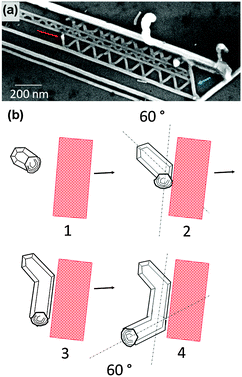 | ||
| Fig. 7 (a) Change in the growth direction due to artificial barriers. This image also highlights the impact of hexagonal structure of the GaN substrate on the growth direction. (b) SEM data supports a sequence of events in which the Au droplet moves to a neighboring facet upon encountering an external surface. Each Au droplet migration results in a 60° rotation in the growth direction. | ||
![Controlling the number of nanowire growth directions in an assembly of Au droplets. (a) An array of ZnO islands arranged in [11̄00] direction of a GaN surface. Each island has six potential growth directions. Steric hindrance and gas flow direction can be used to reduce the number of growth directions from six to two. An example is shown in (b) where the nanowires assembly only shows two major growth directions.](/image/article/2013/CS/c2cs35164a/c2cs35164a-f8.gif) | ||
| Fig. 8 Controlling the number of nanowire growth directions in an assembly of Au droplets. (a) An array of ZnO islands arranged in [100] direction of a GaN surface. Each island has six potential growth directions. Steric hindrance and gas flow direction can be used to reduce the number of growth directions from six to two. An example is shown in (b) where the nanowires assembly only shows two major growth directions. | ||
The growth of horizontal ZnO nanowires can also be controlled in the direction normal to the substrate for making 2D-nanostructures. This can be achieved by combining the SVLS and VS growth processes. In this combination, as the nanowire grows on the substrate surface, the slow VS growth takes place on the (0002) facet of a nanowire, resulting in nanowalls with pristine surfaces, shown in Fig. 9a. As illustrated in Fig. 9b, nanowalls are typically about 80 nm to 100 nm in width and few microns in height. The VS growth starts as soon as a nanowire initiates its lateral growth on the surface. As such, their height is maximum at the initial growth site and minimal at the leading end of the nanowall. Nanowalls are commonly observed when an Au layer thicker than 20 nm is used as catalyst. It is possible that the Au clusters or atoms deposited on the ZnO (0002) plane act as promoters for the catalytic growth process in the [0001] direction of the nanowire. This type of growth has also been observed in the formation of ZnO nanocantilevers and found to be due to the formation of Zn clusters on the (0002) polar surface of the ZnO nanowires.27
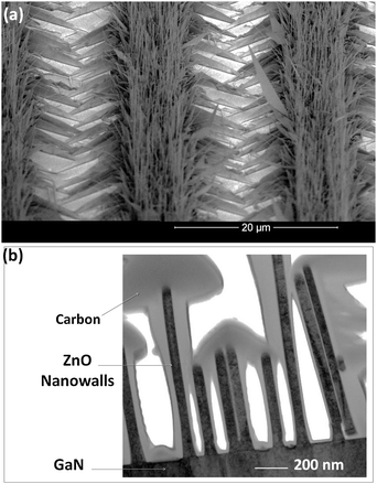 | ||
| Fig. 9 An oblique view of arrays of ZnO nanowalls grown on GaN. Free-standing nanowires are also grown from Au droplets inside the patterns. (b) TEM cross-section of nanowalls shows the elongation of their second dimension along the ZnO polar direction; their narrow width distribution of nanowalls is also noticeable. | ||
The polar surface of ZnO nanowires is formed due to the asymmetric atomic structure of ZnO along its c-direction. The growth in this direction is faster, and as a result, the common growth direction of hexagonal structures like ZnO is [0002] (the c-axis). Such structures are useful in piezoelectric applications, but are not desired for applications where high efficiency of radiative recombination of electron–hole pairs is critical. This is because the strain-induced piezoelectric fields reduce recombination via spatial separation of electrons and holes.102,103 As such, the growth of nonpolar substrates or facets have become of great interest for improving the efficiency of light emitting devices. Results show two types of side facets for ZnO nanowalls. In one group, they are confined to nonpolar a-planes (110) that are upright in orientation (Fig. 9b); in another group, they are confined to semi-polar facets that are slightly inclined giving the nanowalls a triangular cross-section. Both groups of facets are flat originating from the semi-polar side walls of (112) shown in Fig. 5(b).99 This is an important characteristic, as the smoothness and angle of the crystal facets are of great importance for the realization of low loss cavities or waveguides in electro-optical devices.103 To make non-polar facets, there are conventional techniques, such as cleaving crystals and chemical etch; however, they become more challenging as facet size becomes small. Recently, to fabricate arrays of non-polar nanoscale facets of GaN, nanopatterning using electron-beam lithography was used to open nucleation sites on a masked sapphire substrate. GaN nanosheets were then grown epitaxially on the sapphire, which can be used for growth of quantum wells and other heterostructures.102 Laterally grown nanowalls could be of interest in 3D-architectures where the height of the nanoobjects is of significance; for instance, in applications where a higher surface area or a larger light absorption cross-section is desired. In the following sections some of these architectures are described with potential applications in light and energy generators and photocatalysis.
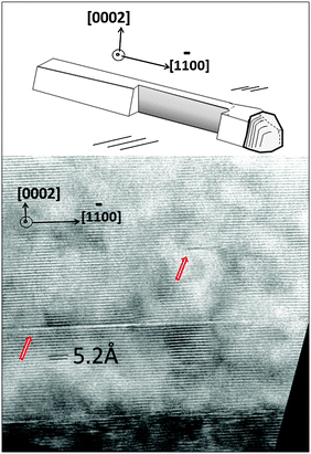
Sapphire, due to its dielectric properties and high thermal conductivity, is a commonly used substrate for the growth of large band-gap semiconductors for light emitting devices and high power electronics. The lateral growth of ZnO nanowires on the a-plane of sapphire results in nanowires with a diameter ranging from 1 nm to 100 nm. As described previously, the diameter of nanowires is correlated with the size of the Au nanodroplets, and therefore can be reasonably controlled.82 Post-growth TEM analyses show that sapphire undergoes a substantial deformation at its interface with ZnO, which includes compressed and expanded regions. The sapphire crystal reconstructs, forming V-shaped interfaces with the nanowires in order to lower its lattice mismatch (Fig. 10a). ZnO, also experiences a strain, which is diameter dependant. As the diameter of the nanowire increases above about 25 nm, it partially or fully relaxes its strain, the V-shaped interface appears more flat, and ZnO facets become well-developed (Fig. 10b).99 The side facet angle with the surface normal is about 32°, which is similar to the structure observed for ZnO nanowires on GaN (Fig. 5). In most studied cases, as the diameter of the nanowire decreases, a compressive strain develops along the [0001] direction, which reaches approximately 7% or less at the base of the nanowire. This is an indirect indication of the expansion of the nanowire at its base in order to minimize its lattice mismatch with the sapphire.
![Cross-sections of small and large size ZnO nanowires grown on a-plane sapphire. (a) Cross-section of a nanowire with ≈10 nm diameter shows the crystal orientation of the two crystals with respect to each other: c-plane of ZnO perpendicular to the c-plane of sapphire. Sapphire in its [0003] direction undergoes a considerable amount of strain to lower its mismatch with ZnO. Part of this strain leads to the reconstruction of sapphire around the nanowire creating a false perception that the ZnO has penetrated into the sapphire. (b) Large diameter ZnO nanowires show a more relaxed ZnO lattice with well-developed facets. The semi-polar side facet is tilted 32° from surface normal. (c) In ZnO, the lattice spacing decreases from top to its base at the interface indicating a lattice compression in the c-direction.](/image/article/2013/CS/c2cs35164a/c2cs35164a-f10.gif) | ||
| Fig. 10 Cross-sections of small and large size ZnO nanowires grown on a-plane sapphire. (a) Cross-section of a nanowire with ≈10 nm diameter shows the crystal orientation of the two crystals with respect to each other: c-plane of ZnO perpendicular to the c-plane of sapphire. Sapphire in its [0003] direction undergoes a considerable amount of strain to lower its mismatch with ZnO. Part of this strain leads to the reconstruction of sapphire around the nanowire creating a false perception that the ZnO has penetrated into the sapphire. (b) Large diameter ZnO nanowires show a more relaxed ZnO lattice with well-developed facets. The semi-polar side facet is tilted 32° from surface normal. (c) In ZnO, the lattice spacing decreases from top to its base at the interface indicating a lattice compression in the c-direction. | ||
In contrast to sapphire, ZnO and GaN exhibit the same wurtzite crystal structure and have very similar lattice constants. GaN is a direct bandgap semiconductor and, with an electron–hole binding energy of about 24 meV is one of the widely used materials in light emitting diodes. ZnO, with a direct bandgap of about 3.3 eV, has attracted a lot of interest for UV light emission, lasing, piezoelectric devices,104 transparent circuitry,105 and photovoltaics.30 Its band gap can be engineered by the addition of Mg or Cd dopants, which are inexpensive and abundant.106 More importantly, ZnO exhibits one of the highest exciton binding energies (about 60 meV), which makes it a great material for high efficiency UV-visible light emitters compared to GaN. ZnO films have been typically grown by techniques such as chemical vapour deposition, pulsed laser deposition, sputtering, and molecular beam epitaxy.107 In the case of epitaxial growth on GaN, a commonly observed characteristic has been the existence of large amount of defects or threading dislocations either extending from the GaN substrate or originated at the interface.108 A similar behaviour is observed in homoepitaxial growth of GaN, and as such there is a great desire to develop growth methods with a reduced number of threading dislocations and other defects that enhance the radiative recombination of charge carriers.109 As discussed later, the SVLS growth of ZnO nanostructures on p-GaN produces formation of abrupt and high quality heterojunctions with no detectable threading dislocation96 that offers new possibilities in integrating 1D- and 2D-ZnO nanostructures to the nitride family of semiconductors such as GaN or InGaN for realization of multi-color light sources at large- or nanoscales.
Heterojunctions of ZnO nanowires and nanowalls with p- and n-GaN have been examined from three different perspectives: normal to the growth direction, tilted 30° from the growth direction, and top view. A representative cross-section of a ZnO nanowire on GaN is shown in Fig. 11a, accompanied by its schematic in Fig. 11b for a better illustration. After the specimen is tilted, the plane of view becomes (zone axis) [110] at which the ZnO plane spacing is larger, thus allowing for easier detection of interface defects. Examining the ZnO–GaN heterojunctions using HRTEM shows a fairly coherent relationship at the interface (Fig. 11c). The SAED pattern shown in the inset shows the c- and m-directions of the ZnO nanocrystal; it also indicates an epitaxial relationship between the two crystals and a single crystal structure. The top view cross-section of a laterally grown ZnO nanowire on GaN is shown in Fig. 12a in which part of a nanowire as well as the Au nanodroplet at its end can be seen. The low magnification image provides some information about the longer range quality of such nanowires and the lack of defects such as twin structures or a poly-crystalline phase as the nanowire grows segment by segment (refer to Section 3.1.3). HRTEM of part of the nanowire in Fig. 12b shows the hexagonal order of atoms in the c-plane of ZnO and GaN. The inset diffraction pattern is consistent with the results obtained from side cross-sections indicating an absence of detectable defects. ZnO nanowalls were examined in the same manner. As described earlier, a nanowall is a result of the nanowire growth in its c-direction. Their structural analyses are similar to the nanowires. HRTEM examination of their interfaces indicate that the single crystal ZnO maintains the orientation of the GaN substrate, namely, (0002)ZnO∥(0002)GaN and [100]ZnO∥[100]GaN. Results also show nearly coherent and abrupt interfaces without formation of an amorphous GaO layer or any reaction layer despite the high growth temperature (900 °C).99
![(a) TEM image of a ZnO nanowire–GaN interface 30 degrees tilted relative to the optic axis. (b) This cross-section is viewed from [112̄0] zone axis. (c) HRTEM image of the ZnO–GaN junction highlighted in part (a) and its SAD pattern in the inset. The heterojunction interface is shown with an arrow. The SAD pattern supports an epitaxial relationship between the two crystals.](/image/article/2013/CS/c2cs35164a/c2cs35164a-f11.gif) | ||
| Fig. 11 (a) TEM image of a ZnO nanowire–GaN interface 30 degrees tilted relative to the optic axis. (b) This cross-section is viewed from [110] zone axis. (c) HRTEM image of the ZnO–GaN junction highlighted in part (a) and its SAD pattern in the inset. The heterojunction interface is shown with an arrow. The SAD pattern supports an epitaxial relationship between the two crystals. | ||
 | ||
| Fig. 12 (a) Top-view cross-section of a horizontally grown ZnO nanowire on GaN. SAED pattern from this perspective also confirms a single crystal structure. ZnO and GaN diffraction spots overlap with each other, because of the similarity of the two crystals. HRTEM image of the marked box interface shown in part (b) denotes only the hexagonal close-pack of atoms as well as a subtle contrast difference between the two sections. | ||
Cross-sectional analysis of nanowalls along their length can provide useful information such as how the defects propagate along the growth direction as new islands gradually form. Since this is a successive growth process, the crystal quality that is observed in one segment of a nanowire or nanowall is expected to be a representative of the ZnO–GaN heterojunction throughout the nanostructure. In most examined regions, ZnO exhibits a crystal structure with no detectable defects such as twin boundaries.110 Scattered stacking faults are observed that appear to be parallel to the interface (arrows in Fig. 13); such defects have been previously observed in free standing nanowires grown in their c-direction.111 Observation shows that the stacking faults are local and do not propagate along the nanowires or nanowalls as new segments are added to the nanowire.
 | ||
| Fig. 13 (Top) Schematic of a nanowire cross-section along its length, which is shown at the bottom. In general, the examined cross-sections show a small variety of defects in the ZnO region. The HRTEM image shows two stacking faults (red arrows) in the ZnO region that do not fully glide through the crystal. Two crystallographic directions are shown in both graphs to better portray the position of the interface. The darker part of the image represents the GaN side. | ||
Furthermore, with respect to misfit dislocations at the interface, we observe a small number of them. In a fully relaxed ZnO thin film on GaN, the 1.8% lattice mismatch is expected to result in formation of misfit dislocations at every 15.8 nm (along 〈100〉), which is not observed in the studied cross-sections.99 This indicates a partial lattice relaxation that also agrees with the observed strain at the interface. Therefore in each 20 nm segment along the length of the nanowalls or nanowires, we estimate to have coherent regions with stored strain, and partially relaxed regions. We did not observe extension of defects such as threading dislocations to the ZnO phase, which is a distinct advantage of one-dimensional ZnO–GaN heterojunctions. This type of defect is notorious in creating non-radiative recombination centers and reducing the performance of light generation in electro-optical devices such as LEDs.109 Overall, in comparison with the thin ZnO films grown at the interface between free standing ZnO nanowires and GaN, the results herein show that the SVLS method leads to significantly lower structural defects.112
3.3 Growth modes of vertically aligned nanowires
Growing vertically aligned nanowires has shown great promise for designing and fabricating novel nanowire-based electrical, optical, and piezoelectric devices.113–115 Such devices would potentially offer higher performance compared to conventional 2D thin film devices. As discussed in earlier sections, the aligned morphology can be controlled by the epitaxial relationship with the single-crystal substrate116 or the deposited nanocrystal seeds on the substrate.117 In most cases, the supporting substrates are different materials from the nanowires due to factors such as substrate availability or the demands of the application. For example, ZnO nanowire arrays have been grown on GaN, AlN, SiC, Si, and sapphire substrates.118 Vertical alignment of ZnO nanowires was first demonstrated on a-plane orientated sapphire substrates.115 In this technique, growth is initiated and guided by Au nanoparticle catalysts and the epitaxial relationship between ZnO and sapphire leads to the alignment. In 2004, Wang et al. combined a self-assembly masking technique with surface epitaxial confinement to grow vertically aligned ZnO nanowires with hexagonal patterns in large areas (Fig. 14a).113 In this approach, a monolayer of close-packed polystyrene nanospheres was self-assembled on a sapphire substrate, acting as a shadow mask for Au catalyst deposition. After the nanospheres were etched away, hexagonal Au patterns were left on the substrate, from which hexagonal arrays of ZnO nanowires were grown via the VLS process.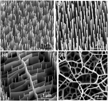 | ||
| Fig. 14 (a) Vertically aligned and hexagonally patterned ZnO nanowires grown on sapphire substrate. (b) Randomly distributed aligned ZnO nanowires grown via VS process. (c) Parallel ZnO nanofin structures. (d) Randomly distributed ZnO nanowall networks. | ||
VS growth process can be utilized in aligned growth of ZnO nanowires without introducing metal catalyst nanoparticles. It is believed that this process is preceded by the random precipitation of Zn clusters from the vapour phase, and thus no control over the distribution of nanowires is possible in this case (Fig. 14b). When the temperature is sufficiently high, the Zn cluster can move laterally across the substrate during the ZnO deposition. As such, ZnO is deposited along the drifting path and the nanowire morphology is converted to vertical ZnO nanofin arrays.119 Similar to nanowalls described in the previous section, the nanofin structure can be as tall as the nanowire (several micrometers) with a thickness of only tens of nanometres. Typically, termination of the nanofin occurs when it reaches a junction with the side wall of a nanowire, where the two structures merge. The spatial distribution of the ZnO nanofins can be controlled by designing a surface feature that would define the drifting path of the Zn clusters. By first depositing a “hill” shaped ZnO epitaxial base layer, most Zn clusters are nucleated along the central line at the summit of the “hill”. Following the inclined base surface, Zn clusters drift to the bottom of the “hill” and initiate the formation of ZnO nanofins that are approximately parallel to each other, as shown in Fig. 14c. Due to the existence of a central wall, which possibly results from the dense nucleation sites along the summit, the vertical nanofins exhibit a more uniform height from their original positions to their termination where it reaches another nanowire. When the substrate is flat, drifting of Zn clusters becomes completely random and is controlled by Brownian motion. A high density of the Zn clusters would also make nanofins quickly intersect with each other, terminating the growth process and resulting in a network (Fig. 14d) that can be considered as traces of the drifted Zn clusters. Due to intersection, the drifting stops quickly and the Zn clusters start to grow into vertical ZnO nanowires. Because of the higher vapour concentration and the small distance between ZnO nanowires, the space between them could be quickly filled by a thin wall of ZnO. Therefore, led by the growth of nanowires, a continuous nanowall network could be formed (Fig. 14d). Since the nanowall locations follows the Brownian motion traces of the mobile Zn clusters, their distribution should not follow the substrate lattice.
A wide range of nanowire–substrate combinations have been generated capable of producing free standing nanowire arrays. Germanium, silicon and InAs nanowires have been grown on Si substrates.120,121 GaAs and InGaAs have both been reported as substrates for InAs nanowire arrays.122 GaN nanowire arrays have been grown on SiC.123 This list is by no means exhaustive, but gives a general feel for the versatility of the technique across a large grouping of materials.
While the range of material combinations that have been demonstrated to be capable of yielding vertical nanowire arrays is impressive, a thorough understanding of how to grow uniform, well-controlled, and perfectly aligned nanowire arrays has not yet been achieved. For example, the size of nanowires is typically defined by the size of metal catalyst nanoparticles used; however, the small lattice mismatch between the nanowires and the substrate is believed to make a significant contribution to the final nanowire morphology. In this regard, the lattice mismatching effect was recently investigated by adapting the Stranski–Krastanow (SK) thin film growth model to understanding the epitaxial growth phenomena of nanowires on heterogeneous substrates.124
For nanowires grown epitaxially on heterogeneous substrates, three growth behaviours have been identified. First, nanowires can grow vertically on a thin film of the same material formed on the surface of the substrate (Fig. 15a). This film serves as a buffer layer and nanowires grown from it should thus be considered as having undergone homo-epitaxial growth. The high density of nucleation sites due to dense catalyst coverage and high vapour concentration of the source gas is believed to be the main reason for the formation of this film. Fig. 15d shows such a situation where vertical ZnO nanowires grew on a very thin layer of a ZnO network. The size of these nanowires exhibits a wide distribution, due to the lack of uniformity in the nucleation sites. In addition, the Au catalyst droplets can be clearly seen on top of these nanowires, indicating that they were formed via a VLS process. Most vertically aligned ZnO nanowires synthesized by vapour deposition belong to this mode, where a thick defective ZnO thin film is always present beneath the vertically oriented, strain-free ZnO nanowires.112 Due to the appearance of a defective heteroepitaxial thin film (or continuous network) prior to the nanowire formation, this growth behaviour is attributed to the general SK mode.
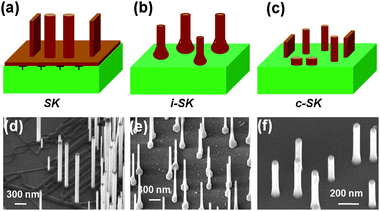 | ||
| Fig. 15 Three suggested heteroepitaxial growth modes of nanowires. (a) The SK mode, where a defective film forms between the solid substrate and strain-free nanowires. (b) The island SK (i-SK) mode, where a cone-shaped base forms beneath the nanowire. (c) The coherent SK (c-SK) mode, where dislocation-free nanowires directly grows on the substrate surface without any intermediate structure. (d–f) Typical SEM images showing ZnO nanowires grown on GaN substrate via the SK, i-SK, and c-SK modes, respectively. | ||
Under other conditions, a large, cone-shaped base would form beneath a long, vertical ZnO nanowire with a uniform diameter (Fig. 15b). Experimental observations show that the diameter of nanowires grown in this mode is smaller and the size distribution narrower than those grown in the SK mode. This mode is commonly observed when vertically aligned nanowires are grown discretely (Fig. 15e). Similar to the case of the continuous film, the large base beneath the nanowire may also contain dislocations in order to reduce the misfit strain energy at the interface. Therefore, this behaviour is simply a modified SK mode, and is normally referred to as the island SK (i-SK) mode.
The least observed growth phenomenon occurs when vertical nanowires grow on a bare substrate surface without any transition structures (Fig. 15c). Fig. 15f shows that these types of nanowires exhibit the smallest average size and the narrowest size distribution. Nanowires with such small sizes were generally discovered to be dislocation free, and, accordingly, this growth behaviour is defined as the coherent SK (c-SK) mode. The SK, i-SK and c-SK modes cover all the observed growth phenomena when vertical nanowires are grown epitaxially on heterogeneous substrates. Among them, the c-SK mode is the most desired due to the uniform dimension of each resulting nanowire and the overall nanowire size distribution.
These three growth modes can be defined by a strain versus dislocation (SVD) model, which describes the competition between the strain energy and the dislocation energy at the interface between the nanowire and the substrate. The nanowire length where these two energies become equal is defined as the critical length (H*). Ideally, dislocation-free nanowires with a given radius could only be formed with a length smaller than H*. Calculating H* at different radii generated a series of points that defined the H* versus R relationship, which is shown by the solid diamond markers in Fig. 16. The critical length quickly increases from a few nanometers to infinity, where the nanowire radius is defined as the critical radius. The H*–R curve can be used to predict the growth behaviour and nanowire dimensions. Lengths and radii were measured from ZnO nanowires synthesized from various experimental batches and plotted together with the curve to show how the three growth modes are related to the H*–R curve. All the c-SK-grown nanowires (star markers) lie on the left-hand-side of the curve. This demonstrates that the SVD model is able to predict the critical diameter of dislocation-free nanowires that can be vertically and uniformly grown on heterogeneous substrates.
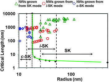 | ||
| Fig. 16 Critical length versus radius plot of dislocation free ZnO nanowires. Triangle, circle, and diamond markers are experimental data measured from ZnO nanowires grown on GaN substrate via SK, i-SK, and c-SK modes, respectively. | ||
The i-SK grown nanowires are marked as circles in the plot. They exhibited larger diameters and are distributed on both sides of the H*–R curve. The increasing trend of the nanowire diameter indicates that the base formed under such nanowires was capable of releasing the interfacial strain energy, thus providing a nearly strain-free, homoepitaxial growth platform. For the nanowires grown via the SK mode, both their diameter and distribution were larger than those measured from the c-SK and i-SK modes. This observation strongly supported the statement that the underlying defective ZnO film accommodated all the compressive strain, and thus nanowires could grow with an “unlimited” length and width. In reality, under these circumstances, the size of nanowires is controlled by the catalyst particles or the fundamental thermodynamic parameters. The relationship between the growth modes and the H*–R curve clearly show that the SVD model is properly established and could serve as an effective guidance for designing vertically aligned nanowires on heterogeneous substrates.
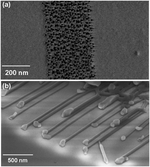
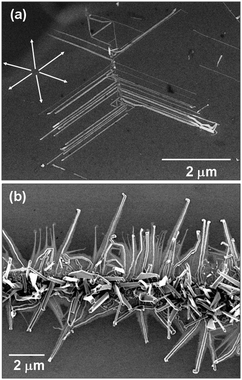
Although these 3D nanowire networks exhibit tuneable electronic properties, the surface area density is still considerably smaller than what can be achieved using 3D nanoparticle networks. Intuitively, a desired improvement would be to increase the volume density of the nanowire branches, resulting in a decrease of the spaces between individual nanowires down to at least the hundreds nanometer regime. Unfortunately, when the spacing scales down from micrometer to sub-micrometer, the growth of nanowire becomes seriously impaired. This is due to the coupling between crystal growth and precursor concentration that is often dictated by the mass flow characteristic of vapour or liquid phase reactants within the highly-confined spaces between nanowires. Recently, Shi et al. developed a surface-reaction-limited pulsed chemical vapour deposition (SPCVD) technique that effectively decoupled the nanowire growth from vapour concentration.135 Through this technique, single-crystalline anatase TiO2 nanowires were uniformly grown covering the entire inner surface of highly-confined anodic aluminium oxide (AAO) nanochannels. The resulting TiO2 nanowire coated AAO channel is shown in Fig. 17. Fig. 17a shows the cross section of the 53 μm-long AAO channels after 660 cycles of SPCVD growth. SEM images acquired from the top, middle and bottom sections are shown in Fig. 17(b–d), respectively, revealing the uniform and dense coverage of TiO2 nanowires along the entire channel length. Closer examination shows that all nanowires were rooted on the walls of the AAO channels and pointed inward (Fig. 17e). The majority of the as-synthesized TiO2 nanowires had lengths and widths of between 170 nm–210 nm and 25 nm–30 nm, respectively. TEM and XRD spectra revealed that the nanowires were single-crystalline anatase TiO2. As shown in Fig. 18, Shi et al. also demonstrated a uniform coverage of TiO2 nanowires on the entire surface of dense Si nanowires.136 The Si nanowires used in the experiments were fabricated by deep reactive ion etching (RIE) using silica spheres as a mask. The lengths of the Si nanowires were ∼15 μm and the spaces in between were 200 nm–300 nm in width. This result demonstrated the versatility of the SPCVD technique for making TiO2 nanowire arrays inside different material matrixes.
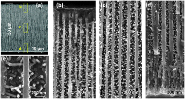 | ||
| Fig. 17 TiO2 nanowires grown in nanochannels. (a) Overview of a cross section of the AAO template after 660 growth cycles. (b–d) Higher magnification SEM images showing the uniform and dense coating of TiO2 nanowires within the AAO channels at the top, middle, and bottom sections, respectively, as indicated by the dashed yellow boxes in (a). (e) TiO2 nanowires rooted on the walls of AAO channels showing a squarelike cross section and well-faceted shape. | ||
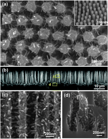 | ||
| Fig. 18 Si nanowire arrays uniformly covered with high-density TiO2 nanowires that grew laterally out of the side surfaces. Inset shows the cross-section of TiO2 nanowire-coated Si nanowire arrays. | ||
The SPCVD technique utilizes separated precursor pulses (TiCl4 and H2O for the growth of TiO2 nanowires) at a relatively high deposition temperature (600 °C). This technique is essentially a successful conversion to anisotropic nanowire growth of the atomic layer deposition (ALD) technique often used for conformal thin-film growth.137 TEM observations and controlled experiments suggested that the formation of nanowire morphology is possibly due to the combined effect of two mechanisms: surface recombination and HCl restructuring. When the temperature is sufficiently high, the surface active species, such as Ti–OH groups, can react among themselves to form inactive Ti–O–Ti bonds in a surface recombination process. Different crystal surfaces would exhibit different reaction rates or activation energies for this recombination reaction, which may lead to the anisotropic growth rate and thus nanowire formation. On the other hand, HCl, a by-product of the deposition reaction, can also react with Ti–O–Ti groups and form Ti–OH and Ti–Cl surface groups. This can be considered as a reactivation process, where the rate is also surface-dependent. These two mechanisms do not conflict with each other and can proceed simultaneously. The combination of these two reactions will cause the active groups to move along the crystal surfaces and reach more stable sites where the recombination rate is low. Therefore, all the TiO2 nanowires were observed to have grown along either the [002] or [011] directions. It would be possible to apply this mechanism to other functional materials that possess similar precursor and surface properties.
4. Challenges in scalable nanodevice integration
4.1. Nanowire-based light emitting devices
Irrespective of the nanodevice size, scaling up device integration requires parallel and high throughput interfacing. In this section, we discuss various designs for charge injection into 1D p–n heterojunctions. Applications are diverse including memory devices, logic circuits, sensory applications, light emitting devices and photovoltaics. In the earlier sections, we described some approaches for controlling the surface registries and orientation of nanocrystals on a given surface. These are some of the prerequisites for device integration if the goal is developing commercially viable technologies. A common goal in integrating nanocrystals to devices is to inject charge carriers to some specific sites. Different strategies have been utilized for integration of nanowire devices. In free-standing nanowire devices, heterojunctions are fabricated at the nanowire interface with the substrate where the charge recombination takes place.138–140 The typical poor quality of this interface can substantially deteriorate the performance of the light emitting device such as its lifetime, operating voltage and emitted wavelengths. In such platforms, the top contact can be placed on nanowires by depositing a conductive contact with a suitable work function to ensure a reasonable ohmic contact. For densely packed standing nanowires, the placement of the top contact requires simple deposition of an inorganic layer.141 For nanowires with a lower packing density, the voids are filled with different non-conducting materials including spin-on-glass,142 or polymers to further stabilize the nanowires.143 One of the limitations of this design is the presence of highly defective ZnO thin film that forms at the interface, despite the typical high quality of the rest of the nanowires.112 In radial heterojunction designs, the active part of the device is the heterojunction between the ZnO nanowires and the counter electrode. The surface area of the heterojunction is a determining factor in the extent of charge recombination or separation in a device and depends on the fabrication process. As an example, in hybrid organic semiconductor-ZnO devices, the p-type polymers can be interfaced with only the top end of the n-type nanowires,144 which results in an overall smaller heterojunction surface area; or it could be interfaced nearly with their entire length by deeper injection of the conductive polymer into the voids between nanowires.145,146 n–p homojunctions of ZnO nanowire have been made axially within the free-standing nanowires. By placing a conductive layer on top and bottom of nanowires their light emission has been demonstrated.147 Challenges in realization of ZnO homojunctions remains to be the difficulty in growing the p-type ZnO layers, and controlling their doping profile with high spatial resolution.148,149 In general, despite high quality of produced ZnO nanowire, their light emitting devices show some common weaknesses such as diversity in their emitted wavelengths and high operating voltages implicating deficiencies in the atomic structure of the device interfaces that must be addressed before realization of their optimal performance.In planar integration of nanowires, the parallel interfacing is not as straightforward as that for the free standing nanowires. This is because the nanowires must be transferred to a target substrate for device fabrication, which requires performing nanowire alignment steps as described in Section 2. The intrinsic limitation of such alignment techniques is the lack of knowledge on the exact location of the active part of a device, e.g., a heterojunction, quantum well or quantum dot. On a small scale, use of single- or multiple nanowire devices (in planar format) have been demonstrated for application such as solar cells,150 and LEDs.151 On a larger scale, serial interfacing of nanowires containing heterojunctions is a slow process and not currently suitable for scaling up as it typically requires a high resolution technique for patterning.152 Pattern transfer techniques have become popular in large scale manipulation of micro- and nano-objects because of their capabilities in parallel interfacing.12,153 These techniques typically require a source substrate that contains the nanostructures, a pattern transfer mean and a target substrate. The minimum size of the formed nanostructures on the target substrate generally depends on the critical dimension of the patterns used in the printing process. As the pattern resolution increases, i.e., toward single nanowire devices, its implementation and nanodevice fabrication becomes more challenging. On a commercial level, these techniques are expected to have a niche in applications where the active elements of the device are groups of nanowires, rather than individual ones. The growing need continues for developing methods with sufficient precisions in positioning and alignment of nanowires down to a single particle level.
The SVLS growth process is expected to have the potential to provide a high precision in determining the registry of the active segment of a device both at single or multiple particle level. In general, the two basic requirements of this process are the deposition of metal catalyst patterns and an appropriate single crystal substrate to guide the growth. In realizing single particle devices on a large scale, the present limiting factor is the need for producing sub-50 nm single particles of the metal catalyst. Given the rapid growth in availability of high resolution microfabrication tools with affordable costs, this limitation is expected to fade away in the near future. Having said that the SVLS technique readily produces 10–20 nanowires per site using typical photolithography tools with a 1 μm resolution.80 In the following, we discuss our recent progress on preparing large arrays of 1D- and 2D-ZnO nanostructure-based light emitting devices on GaN. ZnO has attracted a great deal of interest for UV light emission, lasing, piezoelectric devices,104 “invisible” circuitry,105 and photovoltaics.30 Its band gap can also be engineered by the addition of Mg or Cd dopants, which are inexpensive and abundant.106
Two simple charge injection designs are discussed that both highlight the ability of the SVLS growth process in parallel nanostructure interfacing. In one charge injection scheme as illustrated schematically in Fig. 19a, using the Ti/Au metal contact (yellow bar) electrons are injected to the ZnO backbone and then to the nanowalls, while holes are injected to the underlying p-type GaN substrate using a Ni/Au metal contact. Note that the ZnO backbone is the underlying continuous ZnO film that is formed during the formation of densely packed free-standing nanowires.112 This film forms where the original Au pattern was deposited and possesses approximately the same dimensions. The relative location of nanowall arrays are known with respect to the global marks (not shown here), thus metal contacts can be readily deposited via standard photolithography techniques over the ZnO strips. Representative images of a three-layer (metal/ZnO nanowalls/GaN) structure are shown in Fig. 19(b–c), where the top metal electrode is deposited on the ZnO backbone. The overall shape and size of the nanowire LEDs can be tailored by the original Au pattern, which offers a unique platform for making microscale light sources.96
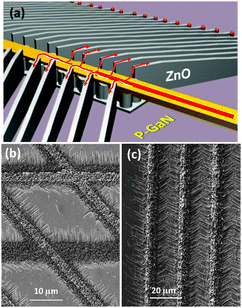 | ||
| Fig. 19 (a) Schematic of the 1st design for charge injection to ZnO nanowalls via a ZnO backbone. As seen in (b–c), the top metal contacts are directly placed on the ZnO backbone. | ||
Fig. 20(a and b), respectively, show the I–V scans of arrays of n–p heterojunctions of ZnO nanowalls on GaN in two large (5 mm × 5 mm) and small (100 μm wide) size devices. The doping level in the GaN layer is about 5 × 1017 cm−3 and the carrier concentration in ZnO is about 1 × 1018 cm−3 based on our previous results.80 Both devices exhibit rectifying behaviors; it is also noted that in the larger device (Fig. 20b) the amount of transported current through the device at a given bias is higher, which is indicative of a larger number of nanowalls as conductive channels. The examined devices exhibit turn on voltages ranging from 2.7 V ± 0.2 V to 3.8 V ± 0.2 V, and breakdown voltages of 3 V ± 0.2 V to 9 V ± 0.2 V. Larger devices also show a lower breakdown voltage, which is mainly attributed to the existence of mid-bandgap states due to the formation of defects at the interface of the ZnO backbone and GaN. As the length of the ZnO backbone is reduced, e.g., in smaller devices, the leakage at the reverse bias is reduced (Fig. 20b).96Fig. 20c shows an optical image of a single array device containing a five millimetre-long ZnO backbone with a polygon shape. This dark pattern is decorated with horizontal nanowalls which are not detectable in this image. Under an injection current of ≈0.9 mA at +7 V, the heterojunctions emit light as seen from the electroluminescence (EL) image in Fig. 20d. Since ZnO is in full contact with GaN, the e–h recombination sites are expected to be along the length of the heterojunctions, which also agrees with the observed emission along both nanowires and nanowalls in the EL images.96 In mechanically formed p–n junctions emission originates from the sites where a nanowire contacts the substrate.151,152 One of the drawbacks of this design is that the injected charges must go through the ZnO strip before reaching the nanowalls. A significant portion of the injected electrons are lost in the ZnO strip mainly due to non-radiative recombination at its interface with GaN. The drop in the injected electrons is such that only the first loop of this device is lit as seen in EL image of Fig. 20d. In addition, the ZnO strip has a certain resistivity that results in heating of the device during operation and thus a lower brightness, as well as potential structural damage.
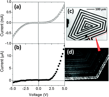 | ||
| Fig. 20 (a) I–V scan of arrays of n–p heterojunctions of ZnO nanowalls on GaN. The overall device size is 5 mm × 5 mm. (b) I–V scan of a small array of n–p heterojunctions of ZnO nanowalls on GaN. The overall device length is 100 μm. (c) Optical image of a 3.6 mm-long array of n–p heterojunctions of ZnO nanowalls on GaN. Nanowalls are grown off of the ZnO backbone, but cannot be resolved in this image. (d) Optical image of this device under forward bias shows that only part of the long array emits light. | ||
An alternative charge injection design is shown in Fig. 21a. In this case, in order to reduce the loss of injected electrons, the top metal contact is directly placed on ZnO nanowalls but without connection to the GaN substrate. In doing so, the electrons are directly transported to the nanowalls and recombine with holes at their intersection with GaN. A representative cross-section of the fabricated devices and its schematic in Fig. 21a shows that a thin dielectric layer such as silicon oxide must be deposited on GaN prior to the placement of the top lead to avoid any short circuit. It is noted that the deposition of the dielectric layer must be unidirectional to ensure the sides of the nanowalls remain uncoated or partially coated. This layer can be seen in Fig. 21a as the dark gray layer above the GaN surface. The sides of the nanowalls before and after silicon oxide deposition are shown in Fig. 21(b–d). By deposition of 125 nm of Ti/Au (15 nm/110 nm) as the top metal contact, the discontinuous oxide-coated side walls are fully coated (Fig. 21a). As shown in Fig. 21d (top), the top contact is deposited photolithographically directly on the nanowalls. Deposition must be performed at two tilt angles to ensure full coverage of nanowall sides with Ti/Au. This is the white layer seen in Fig. 21a, which is viewed from a tilted angle in Fig. 21d. One of the interesting aspects of this design is that the top metal electrode is connected to the non-polar facets of the ZnO in contrast to other designs where the polar facet of the nanowire is in contact. Another distinction is the use of a lower bias voltage for observing the light emission in the second design. Fig. 22(a–e) shows a series of optical images acquired from two sets of devices under a forward bias voltage ranging from 0 V to 12 V. The inset shows a SEM image of one of the devices, which includes two ZnO nanowall arrays, each about 300 μm in length and lateral spacing.
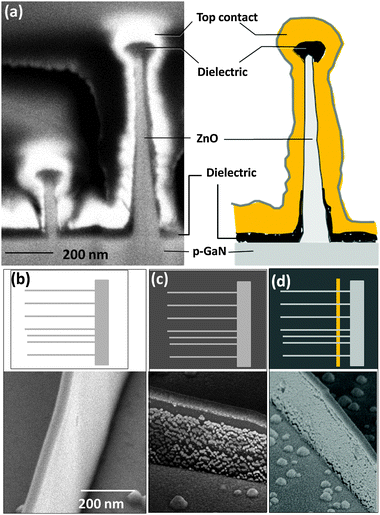 | ||
| Fig. 21 An alternative charge injection design in which nanowalls are directly pumped with electrons. (a) SEM cross-section of two neighboring nanowalls with the corresponding schematic depicting all the device layers. (b) As grown ZnO nanowalls. (c) ZnO nanowalls after overcoating with about 50 nm of silicon oxide; as seen from SEM image, the ZnO side walls are still exposed. (d) Selective deposition of top contact on nanowalls using photolithography. After top contact deposition on nanowalls, the exposed areas of the ZnO side walls are fully coated with metal without any direct electrical contact with the underlying GaN surface. | ||
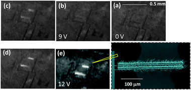 | ||
| Fig. 22 A series of optical images of two parallel devices, which are about 300 μm distant and have a length of about 300 μm. The darker patterns in the images represent the top metal contacts. (a–e) as the forward bias increases from 0 to 12 V, the brightness of the emitting devices increases. Inset of figure (e) is a representative SEM image of heterojunction arrays of ZnO nanowalls on GaN. | ||
The emitted light from heterojunctions can be guided to a spectrometer for characterizing their spectral information. Using both device designs, the EL spectra of a number of heterojunction arrays with different shapes and sizes were studied at different forward and reverse bias voltages from −25 V to 27 V. At forward bias, the common characteristic is a strong excitonic emission at about 390 nm as seen in Fig. 23(a–b) (blue curves). The energy of this emission agrees well with the photoluminescence (PL) of ZnO nanowalls at 380 nm indicating that the recombination of the injected electrons and holes occurs within the ZnO side of the device. This is also in agreement with the observation that light was only emitted from the nanowalls and not from the surrounding GaN substrate (Fig. 20d and 22e). The strong excitonic emission and the absence of deep trap emissions at about 550 nm are both indicative of a low density of traps and defects at the interface. The second design requires a lower bias to operate in comparison with the first design. Furthermore, the breakdown voltage and leakage of the device is substantially reduced as a result of minimizing the contribution of the ZnO backbone in the charge injection process. An example of a sizeable charge transport through the device at the reverse bias voltage is shown in Fig. 20a. At this bias, typically above 6 V, the device emits a bright orange emission centered at about 640 nm (Fig. 23a, yellow curve). This emission is absent in the second diode design (Fig. 23b, yellow curve). This emission is not observed in the PL of the corresponding ZnO arrays on GaN; however, it has been observed in oxygen-rich ZnO films obtained by oxidative annealing.154 The origin of this emission under reverse bias is thought to be a transition from an intrinsic shallow state (such as Zni) to an intrinsic deep state (such as oxygen vacancies in the ZnO). We note that the 640 nm emission intensity drops as the interface area between the ZnO backbone and GaN decreases. EL images at reverse bias show the light is mainly emitted from nanowires or nanowalls thus the e–h recombination is expected to occur in the ZnO layer.96 Based on the energy of this emission at 1.95 eV, its origin is attributed to some mid-gap states in the ZnO. Under reverse bias, electrons from the GaN valence band can tunnel through the depletion region to this mid-gap state and descend to the ZnO valence band resulting in the observed orange emission. It is not clear how nitrogen and oxygen atoms are arranged at the interface, thus the direction of charge transfer and the extent of the depletion of the ZnO/GaN interface is not clear.
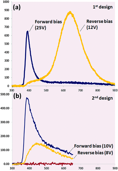 | ||
| Fig. 23 Comparison of the electroluminescence spectra of the two charge injection designs. (a) First design: a 400 nm emission (blue curve) at forward bias is observed, which resembles that of the second charge injection design as shown in graph (b, blue curve). The clear distinction between the two designs is the presence of the 640 nm emission in graph (a) and its absence in the second design (graph b). | ||
As pointed out, the light collection and generation efficiencies in such heterojunctions are directly influenced by the concentration of charge carrier trap sites. The described 1D-heterostructures in comparison with popular thin film LED materials such as III-N family exhibit high quality junctions with substantially reduced defect populations and satisfactory optical properties. The device efficiency is also greatly influenced by the heat generation at the junctions, which is one of the current challenges in thin film LED industries,155 and may be improved by the use of nanowire- and nanowall-based devices due to their larger surface areas and fin-like structures. Although further innovation in design is needed, 1D-nanosystems, benefiting from the rich material combinations and form factor diversity, are expected to offer new solutions as next generation LEDs both at the macro- and microscale.
4.2. Nanogenerators for harvesting mechanical energy
The vertically aligned nanowire morphology allows an entire array of nanowires to be connected in series via top and bottom contacts. This enables the integration of nanowire building blocks into large scale devices; one example of this is the recently developed nanogenerator (NG), which is a device that converts mechanical energy into electricity at the nanometre scale. The operating principle lies on the lateral deflection of piezoelectric nanowires, such as ZnO, which creates positive and negative piezoelectric potential on the tensile and compressive side surfaces, respectively. The NG is assembled by integrating a Pt-coated, serrated electrode with vertically aligned ZnO nanowires, and was demonstrated to convert ultrasonic waves into electricity.156 As schematically shown in Fig. 24a, an array of aligned ZnO nanowires was grown on a GaN substrate and subsequently covered by a serrated Si electrode that had been coated with Pt. The Pt coating not only enhances the conductivity of the electrode, but also creates a Schottky contact at the interface with ZnO. The Schottky contact provides a built-in rectifying effect that only allows electrons to flow from the negatively-charged nanowires to the electrode (forward-biased connection) (Fig. 24b). The top electrode was composed of parallel serrated trenches fabricated on a (001) orientated Si wafer and coated with a thin layer of Pt (Fig. 24c). The electrode was placed above the nanowire arrays and manipulated by a probe station under an optical microscope to achieve precise positioning; the spacing was controlled by soft-polymer stripes deposited between the electrode and the nanowires at the four sides. A cross-sectional image of the packaged nanowire arrays is shown in Fig. 24d. Some nanowires were in direct contact with the top electrode, but some were located between the teeth of the electrode. Under the application of ultrasonic waves, the top electrode would move downward and impinge upon the nanowire leading to a lateral bending. The bending-induced piezoelectric potential would then be collected by the Pt film when the Schottky junction between the nanowire and Pt electrode was forward biased.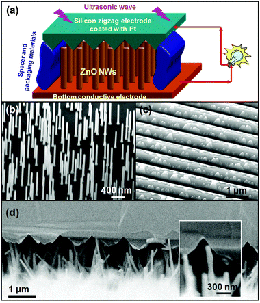 | ||
| Fig. 24 Nanogenerators driven by an ultrasonic wave. (a) Schematic diagram showing the design and structure of the nanogenerator based on aligned ZnO nanowires. (b) Aligned ZnO nanowires grown on a GaN substrate. (c) Zigzag trenched Si electrode coated with 200 nm of Pt. (d) Cross-sectional SEM image of the nanogenerator. Inset: A typical nanowire that is forced by the electrode to bend. | ||
Due to the in situ rectifying effect of the Schottky contact, the detected output electrical signal exhibited a direct current (DC) characteristic. Although each nanowire would still produce electric pulses, accumulation of the output from all nanowire generated a constant DC current signal with large noises, as shown in Fig. 25a. The polarization of the DC signal is consistent with the bias direction of the Pt–ZnO Schottky barrier. When the connection of the electrical measurement system was switched between the two electrodes of the nanogenerator, the polarization of the output signal will be reversed accordingly but the signal amplitude is unaffected, as shown by the black curve in Fig. 25a. This phenomenon further proves the Schottky effect to the nanogenerator output and it is considered as a necessary condition to distinguish valid signals from measurement system artefacts.
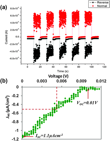 | ||
| Fig. 25 (a) A typical DC current output of an ultrasonic-driven nanogenerator. (b) J–V curve of the nanowire during normal operation, where the short-circuit current and open-circuit voltage can be identified. | ||
The DC output of ultrasonic wave-driven nanogenerators allows for performance characterization by connecting a variable DC voltage source as the load, which is a condition similar to that of solar cell characterization. A typical J–V curve of a nanogenerator is shown in Fig. 25b demonstrating an open circuit voltage of ∼10 mV and a short circuit current density of ∼1 μA cm−2, corresponding to an optimum output power of ∼10 nW cm−2. From the shape of the curve, the fill-factor (FF) was determined to be ∼25%. Thus the operational power of that particular nanogenerator was ∼2.5 nW cm−2. The low FF is likely associated with the large internal resistance due to a large number of branching nanowires and the poor contact between nanowires and the Pt electrode. In an ideal case, if each nanowire is involved in the energy conversion process, the output power could be raised to the μW cm−2 level. Most recently, by integrating a large number of ZnO nanowires in a single NG assembly, the output power has been significantly improved to the μW range and the voltage has been raised to ∼2 V. The relatively high power is already sufficient to support the operation of small electronic devices, such as LEDs, LCDs and nanowire-based sensors.157–159
Compared to conventional thin-film-based piezoelectric cantilever transducers, the use of piezoelectric nanowires for mechanical energy scavenging offers three unique advantages. First, nanowires with a diameter of a few tens of nanometers or less exhibit an enhanced piezoelectric effect when subjected to a non-uniform strain. Secondly, the lattice perfection of nanowires enables much larger critical strain, higher flexibility, and longer operational lifetime. Finally, their large aspect ratio and small thickness allow the creation of significant strain in the nanowires under a force at the nanonewton or even piconewton level. Therefore, with the improvements in nanowire alignment and large-scale fabrication strategies, the NG will fundamentally improve the mechanical energy harvesting capability. This may eventually lead to an effective power source for self-powered electronic systems with higher energy density, higher efficiency, longer life time, as well as lower cost.160
4.3. Photoelectrochemical electrodes (PEC)
High density tree-like 3D nanowire arrays can offer long optical paths for efficient light absorption, high quality one-dimensional (1D) conducting channels for rapid electron–hole separation and charge transport, as well as high surface areas for fast interfacial charge transfer and electrochemical reactions. Therefore, they are considered as an ideal architecture for high-performance PEC electrodes. Using a TiO2–Si heterogeneous 3D nanowire network, enhanced PEC efficiency for photocatalytic water splitting reactions was demonstrated.136 Fabrication of 3D TiO2–Si nanowire architecture is schematically illustrated in Fig. 26a. First, vertical Si nanowire arrays were prepared by selectively etching a heavily-doped n-type Si substrate. Second, high density TiO2 nanowires were uniformly grown around the Si nanowires via the SPCVD process. Lastly, an additional thin film of anatase TiO2 was coated on the nanowire heterostructure by ALD to completely cover Si nanowire surfaces. As schematically shown in Fig. 26b, when this heterogeneous structure is used as a PEC anode for water splitting, photocatalyzed H2O oxidation reactions would only occur on the TiO2 surfaces. In principle, the photo-generated electrons should quickly be transported through the Si nanowire backbone and reach the counter electrode with minimal losses owing to the high conductivity of Si nanowires and isolation from the electrolyte. The very large surface area provided by the TiO2 nanowire arrays together with the high-speed electron transport channels provided by the Si nanowires are promising features that could lead toward a significant improvement of PEC efficiency.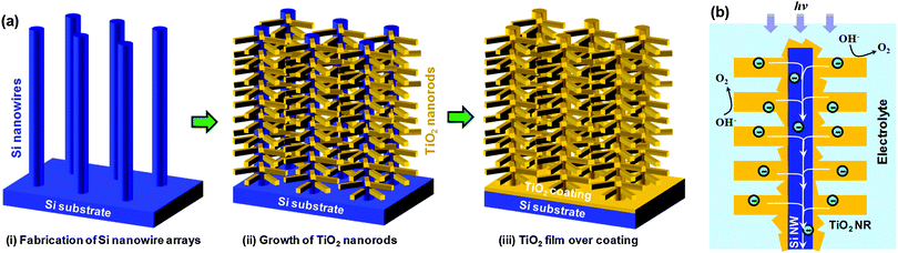 | ||
| Fig. 26 (a) Schematic procedures for making treelike TiO2–Si nanowire 3D architectures. (b) Schematic illustration of using TiO2–Si nanowire heterostructure as PEC anodes for water splitting reactions. | ||
The Si nanowire backbones were fabricated by either RIE dry-etching or metal-assisted wet-etching. The 3D nanowire network structure based on dry-etched Si nanowires has been shown in Fig. 18. High density TiO2 nanowires were deposited on wet-etched Si nanowires. Fig. 27a is a planar view of a wet-etched Si nanowire forest after the growth of these nanowires. Closer examination showed that the Si nanowires were very thin and exhibited irregular cross sectional diameters as highlighted by yellow dashed circles in the inset of Fig. 27a. While the open spaces left within the bundling area were very small, the TiO2 nanowires could be found filling all these spaces. These TiO2 nanowires are 30 nm ± 6 nm in diameter and 243 nm ± 31 nm in length. Fig. 27b shows that the Si nanowires were ∼25 μm in length, where the top portions (a few μm long) were bundled together. Below the bundles, Si nanowires are evenly distributed, providing a good template for conformal nanowires growth. Fig. 27(c–d) are two representative images indicating that the density and dimensions of TiO2 nanowires were nearly identical at the middle and bottom regions. The nanowires grew laterally from the Si nanowires and filled out the interspaces. Thus, a structure exhibiting a considerably large surface area as well as high porosity was created by such a 3D architecture.
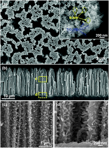 | ||
| Fig. 27 TiO2 nanowires grown on vertical Si nanowire arrays fabricated by wet etching. (a) Top view of Si nanowires after TiO2 nanowire growth. Inset is a higher-magnification SEM image showing TiO2 nanowires growing laterally around Si nanowires. (b) Cross-section of vertical Si nanowire arrays covered with TiO2 nanowires. The Si nanowires are ∼25 μm long and the top ∼5 μm region was bundled together. (c,d) The middle and bottom portions of Si nanowires show dense and uniform coverage of TiO2 nanowires along the entire nanowire length. | ||
The TiO2–Si nanowire 3D architectures were then used as a PEC anode for water oxidation in a 1 M KOH electrolyte using a three-electrode electrochemical cell configuration. Typical plots of photocurrent density versus bias potential are shown in Fig. 28a. The dark current density remained at a very low level (<10−2 mA cm−2) under bias potentials between −1.2 V and 0.5 V (vs. SCE) indicating the high quality of the crystal surfaces of TiO2. The merits of the 3D nanowire networks as PEC anodes were demonstrated by comparing the performance of three TiO2–Si nanowire-based configurations. They are wet-etched Si nanowires with TiO2 nanowires, dry-etched Si nanowires with TiO2 nanowires, and wet-etched Si nanowires. All the Si nanowire templates were 10 μm long. The three plots followed the same trend and exhibited the same VOC (open circuit voltage); while JSC (short circuit current density) varied widely for these samples. The TiO2 thin-film-coated Si nanowires produced a JSC of ∼0.66 mA cm−2. Both nanowire coated samples exhibited significantly higher JSC owing to their larger surface areas. Because the density of wet-etched Si nanowires was higher than that of dry-etched Si nanowires, it yielded the highest JSC (∼1.43 mA cm−2), which was more than twice that produced by the thin-film-coated sample.
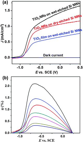 | ||
| Fig. 28 (a) J–E curves and dark currents of different TiO2–Si nanowire (NR) configurations showing enhanced PEC performance by introducing high-density TiO2 nanowire branches. (b) Efficiency vs. bias potential of different TiO2–Si nanowire configurations. The curves from top to bottom are measured from: TiO2/20 μm Si nanowire/250 cycles overcoating, TiO2/20 μm Si nanowire/375 cycles overcoating, TiO2/10 μm Si nanowire/205 cycles overcoating, TiO2/10 μm Si nanowire/375 cycles overcoating, TiO2/10 μm Si nanowire (dry etched)/375 cycles overcoating, 10 μm Si nanowire/375 cycles overcoating, and TiO2/1.5 μm Si nanowire/375 cycles overcoating, respectively. | ||
The PEC performance was further investigated from various 3D nanowire geometries, including different Si nanowire lengths and thickness of TiO2 over-coating (a necessary treatment in order to isolate Si from the electrolyte). From the resulting J–V curves, the PEC efficiencies were also evaluated via the equation:
| η(photo)% = jp(E0rev − |Ebias − Eaoc|) × 100/I0 | (1) |
Using high-density 3D nanowire networks opens a new avenue toward high-performance electrode design, and could show substantial impacts on energy harvesting and storage devices. For example, V2O5 is widely investigated as a promising cathode material in lithium ion batteries.44–46 However, the poor electrical conductivity and low diffusion rate of Li+ ions in V2O5 have stimulated the interest in nanowire morphologies which reduce the electron and ion diffusion length and enhance the power density. A 3D nanowire structure such as that presented in Fig. 26 is therefore ideal. The backbone nanowires are responsible for the high rate of charge transport, while the V2O5 nanowire branches are responsible for ion intercalation originating in the increased accommodations of transformational strain compared to their bulk counterpart. SPCVD is a powerful approach to producing this complex nanowire structure by choosing suitable precursors that do not decompose at high temperature. WO348–50 and Fe2O351–53 are well-known photocatalysis materials due to their small band gaps, proper band alignments with water redox potentials and low cost. However, both materials are subject to short carrier diffusion length, resulting in very poor quantum efficiency. 3D nanowire structures are also beneficial to their catalytic applications since the charge collection efficiency and surface area could both be dramatically enhanced. With the SPCVD approach, branched nanowires formed of WO3 and Fe2O3 could be synthesized to escalate the surface area for efficient light absorption and surmount the charge transport problem via the highly-conductive backbone nanowires.
5. Conclusion
A detailed review on self-aligned and vapor-based growth of 1D-nanostructures of ZnO, TiO2 and related materials is given. Some of the main demands of the nanotech industry in nanowire device integrations and applications are highlighted and limitations are discussed. Different growth mechanisms are explored and their advantages in interfacing nanowires to outside world are presented. The strength of the SVLS growth technique is in its high precision in controlling the hierarchy of nanowires and in large scale charge injection into planar arrays of 1D- or 2D-nanostructures. SPCVD technique offers a new capability to grow uniform nanowire branches inside high-density nanowire arrays. Understandings of these growth mechanisms and application potentials have led and will continuously lead to many new advancements for other functional nanomaterials, including WO3,48–50 SnO2,41–43,161 V2O5,44–46 and Fe2O351,52 to name but a few. The high quality of the interfaces, well-controlled and aligned morphology, and extremely large surface area offers a high level of fidelity in their use in future nanotechnologies including electronic and optoelectronic devices, energy harvesting, conversion and storage systems.Acknowledgements
BN wishes to thank Dr S. Eustis for collecting some of the TEM images. XW and JS thank the support UW-NSF Nanoscale Science and Engineering Centre (NSEC) (DMR 0425880) and UW graduate school.Notes and references
- W. Arden, M. Brillouët, P. Cogez, M. Graef, B. Huizing, and R. Mahnkopf, More-than-Moore white paper, 2010, p. 8 [http://www.itrs.net].
- B. Nikoobakht and X. L. Li, ACS Nano, 2012, 6, 1883–1887 CrossRef CAS.
- E. Stern, A. Vacic, N. K. Rajan, J. M. Criscione, J. Park, B. R. Ilic, D. J. Mooney, M. A. Reed and T. M. Fahmy, Nat. Nanotechnol., 2010, 5, 138–142 CrossRef CAS.
- P. L. Edwards and R. J. Happel, J. Appl. Phys., 1962, 33, 943–948 CrossRef CAS.
- R. S. Wagner and W. C. Ellis, Appl. Phys. Lett., 1964, 4, 89–90 CrossRef CAS.
- Y. Miyamoto and M. Hirata, Jpn. J. Appl. Phys., 1975, 14, 1419–1420 CrossRef CAS.
- E. I. Givargizov, Highly Anisotropic Crystals, Kluwer Academic Publishers, 1987 Search PubMed.
- Y. M. Tairov, V. F. Tsvetkov and I. I. Khlebnik, J. Cryst. Growth, 1973, 20, 155–157 CrossRef CAS.
- K. Haraguchi, T. Katsuyama, K. Hiruma and K. Ogawa, Appl. Phys. Lett., 1991, 60, 745–747 CrossRef.
- A. M. Morales and C. M. Lieber, Science, 1998, 279, 208–211 CrossRef CAS.
- J. Westwater, D. P. Gosain, S. Tomiya, S. Usui and H. Ruda, J. Vac. Sci. Technol., B: Microelectron. Nanometer Struct.--Process., Meas., Phenom., 1997, 15, 554–557 CrossRef CAS.
- Z. Fan, J. C. Ho, Z. A. Jacobson, H. Razavi and A. Javey, Proc. Natl. Acad. Sci. U. S. A., 2008, 105, 11066 CrossRef CAS.
- X. Duan, C. Niu, V. Sahi, J. Chen, J. W. Parce, S. Empedocles and J. L. Goldman, Nature, 2003, 425, 274–278 CrossRef CAS.
- D. Goldhaber-Gordon, M. S. Montemerlo, J. C. Love, G. J. Opiteck and J. C. Ellenbogen, Proc. IEEE, 1997, 85, 521–540 CrossRef CAS.
- F. Kim, S. Kwan, J. Akana and P. Yang, J. Am. Chem. Soc., 2001, 123, 4360–4361 CrossRef CAS.
- B. Nikoobakht, Z. L. Wang and M. A. El-Sayed, J. Phys. Chem. B, 2000, 104, 8635–8640 CrossRef CAS.
- G. Yu, A. Cao and C. M. Lieber, Nat. Nanotechnol., 2007, 2, 372–377 CrossRef CAS.
- N. A. Melosh, A. Boukai, F. Diana, B. Gerardot, A. Badolato, P. M. Petroff and J. R. Heath, Science, 2003, 300, 112–115 CrossRef CAS.
- A. Javey, S. Woo, R. S. Friedman, H. Yan and C. M. Lieber, Nano Lett., 2007, 7, 773–777 CrossRef CAS.
- A. Pevzner, Y. Engel, R. Elnathan, T. Ducobni, M. Ben-Ishai, K. Reddy, N. Shpaisman, A. Tsukernik, M. Oksman and F. Patolsky, Nano Lett., 2010, 10, 1202–1208 CrossRef CAS.
- E. Saeedi, C. Marcheselli, A. Shum and B. A. Parviz, Nanotechnology, 2010, 21, 375604 CrossRef CAS.
- S. Xu, Y. Ding, Y. Wei, H. Fang, Y. Shen, A. K. Sood, D. L. Polla and Z. L. Wang, J. Am. Chem. Soc., 2009, 131, 6670–6671 CrossRef CAS.
- M. A. Meitl, Z. T. Zhu, V. Kumar, K. J. Lee, X. Feng, Y. Y. Huang, I. Adesida, R. G. Nuzzo and J. A. Rogers, Nat. Mater., 2006, 5, 33–38 CrossRef CAS.
- R. Yerushalmi, Z. A. Jacobson, J. C. Ho, Z. Fan and A. Javey, Appl. Phys. Lett., 2007, 91, 203104 CrossRef.
- K. Takei, T. Takahashi, J. C. Ho, H. Ko, A. G. Gillies, P. W. Leu, R. S. Fearing and A. Javey, Nat. Mater., 2010, 9, 821–826 CrossRef CAS.
- S. A. Morin and S. Jin, Nano Lett., 2010, 10, 3459–3463 CrossRef CAS.
- Z. L. Wang, X. Y. Kong and J. M. Zuo, Phys. Rev. Lett., 2003, 91, 185502 CrossRef CAS.
- B. Gates, B. Mayers, B. Cattle and Y. N. Xia, Adv. Funct. Mater., 2002, 12, 219–227 CrossRef CAS.
- H. Yu and W. E. Buhro, Adv. Mater., 2003, 15, 416–419 CrossRef CAS.
- M. Law, L. E. Greene, J. C. Johnson, R. Saykally and P. Yang, Nat. Mater., 2005, 4, 455–459 CrossRef CAS.
- Y. Qin, R. Yang and Z. L. Wang, J. Phys. Chem. C, 2008, 112, 18734–18736 CAS.
- L. E. Greene, M. Law, D. H. Tan, M. Montano, J. Goldberger, G. Somorjai and P. D. Yang, Nano Lett., 2005, 5, 1231–1236 CrossRef CAS.
- X. J. Feng, K. Shankar, O. K. Varghese, M. Paulose, T. J. Latempa and C. A. Grimes, Nano Lett., 2008, 8, 3781–3786 CrossRef CAS.
- S. A. Morin, M. J. Bierman, J. Tong and S. Jin, Science, 2010, 328, 476–480 CrossRef CAS.
- A. Fujishima and K. Honda, Nature, 1972, 238, 37–38 CrossRef CAS.
- B. Oregan and M. Gratzel, Nature, 1991, 353, 737–740 CrossRef CAS.
- S. Xu, Y. Qin, C. Xu, Y. G. Wei, R. S. Yang and Z. L. Wang, Nat. Nanotechnol., 2010, 5, 366–373 CrossRef CAS.
- S. Xu, Y. Wei, M. Kirkham, J. Liu, W. Mai, D. Davidovic, R. L. Snyder and Z. L. Wang, J. Am. Chem. Soc., 2008, 130, 14958–14959 CrossRef CAS.
- Y. G. Wei, W. Z. Wu, R. Guo, D. J. Yuan, S. M. Das and Z. L. Wang, Nano Lett., 2010, 10, 3414–3419 CrossRef CAS.
- J.-H. Ahn, Y.-J. Kim and G. Wang, J. Alloys Compd., 2009, 483, 422–424 CrossRef CAS.
- A. Kolmakov, D. O. Klenov, Y. Lilach, S. Stemmer and M. Moskovits, Nano Lett., 2005, 5, 667–673 CrossRef CAS.
- S. H. Lee, G. Jo, W. Park, S. Lee, Y.-S. Kim, B. K. Cho, T. Lee and W. B. Kim, ACS Nano, 2010, 4, 1829–1836 CrossRef CAS.
- J. Pan, H. Shen, U. Werner, J. D. Prades, F. Hernandez-Ramirez, F. Soldera, F. Mucklich and S. Mathur, J. Phys. Chem. C, 2011, 115, 15191–15197 CAS.
- H. Liu and W. Yang, Energy Environ. Sci., 2011, 4, 4000–4008 CAS.
- T. Zhai, H. Liu, H. Li, X. Fang, M. Liao, L. Li, H. Zhou, Y. Koide, Y. Bando and D. Golberg, Adv. Mater., 2010, 22, 2547–2552 CrossRef CAS.
- B. Yan, L. Liao, Y. You, X. Xu, Z. Zheng, Z. Shen, J. Ma, L. Tong and T. Yu, Adv. Mater., 2009, 21, 2436–2440 CrossRef CAS.
- C. Diaz-Guerra and J. Piqueras, J. Appl. Phys., 2007, 102, 084307–084304 CrossRef.
- H. Chen, N. Xu, S. Deng, J. Zhou, Z. Li, H. Ren, J. Chen and J. She, J. Appl. Phys., 2007, 101, 114303–114305 CrossRef.
- Z. Gu, T. Zhai, B. Gao, X. Sheng, Y. Wang, H. Fu, Y. Ma and J. Yao, J. Phys. Chem. B, 2006, 110, 23829–23836 CrossRef CAS.
- J. Su, X. Feng, J. D. Sloppy, L. Guo and C. A. Grimes, Nano Lett., 2010, 11, 203–208 CrossRef.
- Y. Fu, J. Chen and H. Zhang, Chem. Phys. Lett., 2001, 350, 491–494 CrossRef CAS.
- G. Wang, X. Gou, J. Horvat and J. Park, J. Phys. Chem. C, 2008, 112, 15220–15225 CAS.
- P. M. Rao and X. Zheng, Nano Lett., 2009, 9, 3001–3006 CrossRef CAS.
- M. T. Bjork, B. J. Ohlsson, T. Sass, A. I. Persson, C. Thelander, M. H. Magnusson, K. Deppert, L. R. Wallenberg and L. Samuelson, Nano Lett., 2002, 2, 87–89 CrossRef.
- F. Qian, Y. Li, S. Gradecak, H.-G. Park, Y. Dong, Y. Ding, Z. L. Wang and C. M. Lieber, Nat. Mater., 2008, 7, 701–706 CrossRef CAS.
- L. J. Lauhon, M. S. Gudiksen, D. Wang and C. M. Lieber, Nature, 2002, 420, 57–61 CrossRef CAS.
- C. Yang, Z. Zhong and C. M. Lieber, Science, 2005, 310, 1304–1307 CrossRef CAS.
- M. S. Gudiksen, L. J. Lauhon, J. Wang, D. C. Smith and C. M. Lieber, Nature, 2002, 415, 617–620 CrossRef CAS.
- X. Wang, J. Song, P. Li, J. H. Ryou, R. D. Dupuis, C. J. Summers and Z. L. Wang, J. Am. Chem. Soc., 2005, 127, 7920–7923 CrossRef CAS.
- B. Tian, P. Xie, T. J. Kempa, D. C. Bell and C. M. Lieber, Nat. Nanotechnol., 2009, 4, 824–829 CrossRef CAS.
- B. Xiang, P. Wang, X. Zhang, S. A. Dayeh, D. P. R. Aplin, C. Soci, D. Yu and D. Wang, Nano Lett., 2006, 7, 323–328 CrossRef.
- Y. Wu, R. Fan and P. Yang, Nano Lett., 2002, 2, 83–86 CrossRef CAS.
- S. A. Fortuna and X. L. Li, Semicond. Sci. Technol., 2010, 25, 24005 CrossRef.
- E. P. A. M. Bakkers, M. T. Borgstrom and M. A. Verheijen, MRS Bull., 2007, 32, 5 CrossRef.
- L. C. Chuang, M. Moewe, C. Chase, N. P. Kobayashi, C. Chang-Hasnain and S. Crankshaw, Appl. Phys. Lett., 2007, 90, 043115 CrossRef.
- Y. Wu, Y. Cui, L. Huynh, C. J. Barrelet, D. C. Bell and C. M. Lieber, Nano Lett., 2004, 4, 433–436 CrossRef CAS.
- C. X. Wang, M. Hirano and H. Hosono, Nano Lett., 2006, 6, 1552–1555 CrossRef CAS.
- V. Schmidt, S. Senz and U. Gosele, Nano Lett., 2005, 5, 931–935 CrossRef CAS.
- J. Stangl, V. Holy and G. Bauer, Rev. Mod. Phys., 2004, 76, 725–783 CrossRef CAS.
- D. J. Eaglesham and M. Cerullo, Phys. Rev. Lett., 1990, 64, 1943 CrossRef CAS.
- Y. Chen, D. A. A. Ohlberg, G. Medeiros-Ribeiro, Y. A. Chang and R. S. Williams, Appl. Phys. Lett., 2000, 76, 4004–4006 CrossRef CAS.
- Y. Chen, D. A. A. Ohlberg and R. S. Williams, J. Appl. Phys., 2002, 91, 3213–3218 CrossRef CAS.
- D. Loretto, F. M. Ross and C. A. Lucas, Appl. Phys. Lett., 1996, 68, 2363–2365 CrossRef CAS.
- Z. A. He, D. J. Smith and P. A. Bennett, Phys. Rev. Lett., 2004, 93, 256102 CrossRef.
- P. A. Bennett, Z. A. He, D. J. Smith and F. M. Ross, Thin Solid Films, 2011, 519, 8434–8440 CrossRef CAS.
- E. I. Givargizov, J. Cryst. Growth, 2008, 310, 1686–1690 CrossRef CAS.
- H. Ago, K. Nakamura, K. Ikeda, N. Uehara, N. Ishigami and M. Tsuji, Chem. Phys. Lett., 2005, 408, 433–438 CrossRef CAS.
- H. Ago, T. Nishi, K. Imamoto, N. Ishigami, M. Tsuji, T. Ikuta and K. Takahashi, J. Phys. Chem. C, 114, 12925–12930 CAS.
- T. Ogino, H. Hibino, Y. Homma, Y. Kobayashi, K. Prabhakaran, K. Sumitomo and H. Omi, Acc. Chem. Res., 1999, 32, 8 CrossRef.
- B. Nikoobakht, Chem. Mater., 2007, 19, 5279–5284 CrossRef CAS.
- S. A. Fortuna, J. Wen, I. S. Chun and X. Li, Nano Lett., 2008, 8, 4421–4427 CrossRef CAS.
- B. Nikoobakht, C. A. Michaels, S. J. Stranick and M. D. Vaudin, Appl. Phys. Lett., 2004, 85, 3244–3246 CrossRef CAS.
- Z. M. Zhu, T. L. Chen, Y. Gu, J. Warren and R. M. Osgood, Chem. Mater., 2005, 17, 4227–4234 CrossRef CAS.
- T. Kuykendall, P. Pauzauskie, S. K. Lee, Y. F. Zhang, J. Goldberger and P. D. Yang, Nano Lett., 2003, 3, 1063–1066 CrossRef CAS.
- S. Y. Li, C. Y. Lee and T. Y. Tseng, J. Cryst. Growth, 2003, 247, 357–362 CrossRef CAS.
- P. X. Gao, Y. Ding and Z. L. Wang, Nano Lett., 2003, 3, 1315–1320 CrossRef CAS.
- V. Schmidt, J. V. Wittemann and U. Gosele, Chem. Rev., 2010, 110, 361–388 CrossRef CAS.
- S. Eustis, L. H. Robins and B. Nikoobakht, J. Phys. Chem. C, 2009, 113, 2277–2285 CAS.
- B. M. Kayes, M. A. Filler, M. C. Putnam, M. D. Kelzenberg, N. S. Lewis and H. A. Atwater, Appl. Phys. Lett., 2007, 91, 103110 CrossRef.
- Z. Wu, M. G. Hahm, Y. J. Jung and L. Menon, J. Mater. Chem., 2009, 19, 463–467 RSC.
- D. Tsivion, M. Schvartzman, R. Popovitz-Biro, P. von Huth and E. Joselevich, Science, 2011, 333, 1003–1007 CrossRef CAS.
- J. Y. Lao, J. Y. Huang, D. Z. Wang and Z. F. Ren, Adv. Mater., 2004, 16, 65–69 CrossRef CAS.
- Z. Zhang, L. M. Wong, H. X. Wang, Z. P. Wei, W. Zhou, S. J. Wang and T. Wu, Adv. Funct. Mater., 2010, 20, 2511–2518 CrossRef CAS.
- M. H. Huang, S. Mao, H. Feick, H. Q. Yan, Y. Y. Wu, H. Kind, E. Weber, R. Russo and P. D. Yang, Science, 2001, 292, 1897–1899 CrossRef CAS.
- P. Fons, K. Iwata, A. Yamada, K. Matsubara, S. Niki, K. Nakahara, T. Tanabe and H. Takasu, Appl. Phys. Lett., 2000, 77, 1801–1803 CrossRef CAS.
- B. Nikoobakht and A. Herzing, ACS Nano, 2010, 4, 5877–5886 CrossRef CAS.
- J. M. Zuo and J. C. Mabon, Web-based Electron Microscopy Application Software: Web-EMAPS, Microsc. Microanal. 10 (suppl 2), 2004, http://emaps.mrl.uiuc.edu/.
- B. Nikoobakht, S. Eustis and A. Herzing, J. Phys. Chem. C, 2009, 113, 7031–7037 CAS.
- B. Nikoobakht, J. Bonevich and A. Herzing, J. Phys. Chem. C, 2011, 115, 9961–9969 CAS.
- L. F. Dong, J. Jiao, D. W. Tuggle, J. M. Petty, S. A. Elliff and M. Coulter, Appl. Phys. Lett., 2003, 82, 1096–1098 CrossRef CAS.
- K. W. Schwarz and J. Tersoff, Nano Lett., 2011, 11, 316–320 CrossRef CAS.
- T. W. Yeh, Y. T. Lin, B. Ahn, L. S. Stewart, P. D. Dapkus and S. R. Nutt, Appl. Phys. Lett., 2012, 100, 33119 CrossRef.
- J. Rass, T. Wernicke, R. Kremzow, W. John, S. Einfeldt, P. Vogt, M. Weyers and M. Kneissl, Phys. Status Solidi A, 2010, 207, 1361–1364 CrossRef CAS.
- Z. L. Wang and J. Song, Science, 2006, 312, 242–246 CrossRef CAS.
- K. Nomura, H. Ohta, K. Ueda, T. Kamiya, M. Hirano and H. Hosono, Science, 2003, 300, 1269–1272 CrossRef CAS.
- S. J. Pearton, W. T. Lim, J. S. Wright, L. C. Tien, H. S. Kim, D. P. Norton, H. T. Wang, B. S. Kang, F. Ren, J. Jun, J. Lin and A. Osinsky, J. Electron. Mater., 2008, 37, 1426–1432 CrossRef CAS.
- H.-J. Ko, S.-K. Hong, Y. Chen and T. Yao, Thin Solid Films, 2002, 409, 153–160 CrossRef CAS.
- T. P. Smith, H. A. McLean, D. J. Smith, P. Q. Miraglia, A. M. Roskowski and R. F. Davis, J. Electron. Mater., 2004, 33, 826–832 CrossRef CAS.
- P. Kozodoy, J. P. Ibbetson, H. Marchand, P. T. Fini, S. Keller, J. S. Speck, S. P. DenBaars and U. K. Mishra, Appl. Phys. Lett., 1998, 73, 975–977 CrossRef CAS.
- F. M. Davidson, D. C. Lee, D. D. Fanfair and B. A. Korgel, J. Phys. Chem. C, 2007, 111, 2929–2935 CAS.
- Y. Chen, B. Qu, Y. A. Barnkov, Q. Tang and J. Chen, J. Mater. Sci.: Mater. Electron., 2009, 20, 326–332 CrossRef.
- I. Levin, A. Davydov, B. Nikoobakht, N. Sanford and P. Mogilevsky, Appl. Phys. Lett., 2005, 87, 103110–103113 CrossRef.
- X. D. Wang, C. J. Summers and Z. L. Wang, Nano Lett., 2004, 4, 423–426 CrossRef CAS.
- H. J. Fan, P. Werner and M. Zacharias, Small, 2006, 2, 700–717 CrossRef CAS.
- M. Huang, S. Mao, H. Feick, H. Yan, Y. Wu, H. Kind, E. Weber, R. Russo and P. Yang, Science, 2001, 292, 1897–1899 CrossRef CAS.
- X. D. Wang, J. H. Song and Z. L. Wang, J. Mater. Chem., 2007, 17, 711–720 RSC.
- L. E. Greene, M. Law, J. Goldberger, F. Kim, J. C. Johnson, Y. Zhang, R. J. Saykally and P. Yang, Angew. Chem., Int. Ed., 2003, 42, 3031–3034 CrossRef CAS.
- X. D. Wang, J. H. Song, P. Li, J. H. Ryou, R. D. Dupuis, C. J. Summers and Z. L. Wang, J. Am. Chem. Soc., 2005, 127, 7920–7923 CrossRef CAS.
- J. Shi, S. Grutzik and X. D. Wang, ACS Nano, 2009, 3, 1594–1602 CrossRef CAS.
- T. Martensson, C. P. T. Svensson, B. A. Wacaser, M. W. Larsson, W. Seifert, K. Deppert, A. Gustafsson, L. R. Wallenberg and L. Samuelson, Nano Lett., 2004, 4, 1987–1990 CrossRef CAS.
- S. Krylyuk, A. V. Davydov and I. Levin, ACS Nano, 2011, 5, 656–664 CrossRef CAS.
- H. Paetzelt, V. Gottschalch, J. Bauer, G. Benndorf and G. Wagner, J. Cryst. Growth, 2008, 310, 5093–5097 CrossRef CAS.
- M. Lei, H. Yang, P. G. Li and W. H. Tang, Appl. Surf. Sci., 2008, 254, 1947–1952 CrossRef CAS.
- J. Shi and X. Wang, J. Phys. Chem. C, 2010, 114, 2082–2088 CAS.
- M. J. Bierman and S. Jin, Energy Environ. Sci., 2009, 2, 1050–1059 CAS.
- P. X. Gao and Z. L. Wang, Appl. Phys. Lett., 2004, 84, 2883–2885 CrossRef CAS.
- J.-P. Ge, J. Wang, H.-X. Zhang, X. Wang, Q. Peng and Y.-D. Li, Chem.–Eur. J., 2005, 11, 1889–1894 CrossRef CAS.
- M. J. Bierman, Y. K. A. Lau and S. Jin, Nano Lett., 2007, 7, 2907–2912 CrossRef CAS.
- J. Zhou, Y. Ding, S. Z. Deng, L. Gong, N. S. Xu and Z. L. Wang, Adv. Mater., 2005, 17, 2107–2110 CrossRef CAS.
- C.-I. Tsai, P.-H. Yeh, C.-Y. Wang, H.-W. Wu, U.-S. Chen, M.-Y. Lu, W.-W. Wu, L.-J. Chen and Z.-L. Wang, Cryst. Growth Des., 2009, 9, 4514–4518 CAS.
- J. Zhu, H. Peng, A. F. Marshall, D. M. Barnett, W. D. Nix and Y. Cui, Nat. Nanotechnol., 2008, 3, 477–481 CrossRef CAS.
- M. J. Bierman, Y. K. A. Lau, A. V. Kvit, A. L. Schmitt and S. Jin, Science, 2008, 320, 1060–1063 CrossRef CAS.
- K. A. Dick, K. Deppert, M. W. Larsson, T. Martensson, W. Seifert, L. R. Wallenberg and L. Samuelson, Nat. Mater., 2004, 3, 380–384 CrossRef CAS.
- D. Wang, F. Qian, C. Yang, Z. Zhong and C. M. Lieber, Nano Lett., 2004, 4, 871–874 CrossRef CAS.
- J. Shi, C. Sun, M. B. Starr and X. D. Wang, Nano Lett., 2011, 11, 624–631 CrossRef CAS.
- J. Shi, Y. Hara, C. Sun, M. A. Anderson and X. Wang, Nano Lett., 2011, 11, 3413–3419 CrossRef CAS.
- S. M. George, Chem. Rev., 2010, 110, 111–131 CrossRef CAS.
- X. W. Sun, J. Z. Huang, J. X. Wang and Z. Xu, Nano Lett., 2008, 8, 1219–1223 CrossRef CAS.
- X.-M. Zhang, M.-Y. Lu, Y. Zhang, L. J. Chen and Z. L. Wang, Adv. Mater., 2009, 21, 2767–2770 CrossRef CAS.
- A. M. C. Ng, Y. Y. Xi, Y. F. Hsu, A. B. Djurisic, W. K. Chan, S. Gwo, H. L. Tam, K. W. Cheah, P. W. K. Fong, H. F. Lui and C. Surya, Nanotechnology, 2009, 20, 445201 CrossRef CAS.
- W. I. Park and G. C. Yi, Adv. Mater., 2004, 16, 4 Search PubMed.
- H.-M. Kim, Y.-H. Cho, H. Lee, S. I. Kim, S. R. Ryu, D. Y. Kim, T. W. Kang and K. S. Chung, Nano Lett., 2004, 4, 1059–1062 CrossRef CAS.
- R. Konenkamp, R. C. Word and C. Schlegel, Appl. Phys. Lett., 2004, 85, 6004–6006 CrossRef CAS.
- R. Konenkamp, R. C. Word and M. Godinez, Nano Lett., 2005, 5, 2005–2008 CrossRef CAS.
- A. L. Briseno, T. W. Holcombe, A. I. Boukai, E. C. Garnett, S. W. Shelton, J. J. M. Frechet and P. D. Yang, Nano Lett., 2010, 10, 334–340 CrossRef CAS.
- C.-H. Chen, S.-J. Chang, S.-P. Chang, M.-J. Li, C. Chen, T.-J. Hsueh and C.-L. Hsu, Appl. Phys. Lett., 2009, 95, 223101 CrossRef.
- M. T. Chen, M. P. Lu, Y. J. Wu, J. H. Song, C. Y. Lee, M. Y. Lu, Y. C. Chang, L. J. Chou, Z. L. Wang and L. J. Chen, Nano Lett., 2010, 10, 4387–4393 CrossRef CAS.
- G. D. Yuan, W. J. Zhang, J. S. Jie, X. Fan, J. A. Zapien, Y. H. Leung, L. B. Luo, P. F. Wang, C. S. Lee and S. T. Lee, Nano Lett., 2008, 8, 2591–2597 CrossRef CAS.
- B. Xiang, P. W. Wang, X. Z. Zhang, S. A. Dayeh, D. P. R. Aplin, C. Soci, D. P. Yu and D. L. Wang, Nano Lett., 2007, 7, 323–328 CrossRef CAS.
- Y. Dong, B. Tian, T. J. Kempa and C. M. Lieber, Nano Lett., 2009, 9, 2183–2187 CrossRef CAS.
- S. K. Lee, T. H. Kim, S. Y. Lee, K. C. Choi and P. Yang, Philos. Mag., 2007, 87, 2105–2115 CrossRef CAS.
- M. A. Zimmler, D. Stichtenoth, C. Ronning, W. Yi, V. Narayanamurti, T. Voss and F. Capasso, Nano Lett., 2008, 8, 1695–1699 CrossRef.
- J.-H. Ahn, H.-S. Kim, K. J. Lee, S. Jeon, S. J. Kang, Y. Sun, R. G. Nuzzo and J. A. Rogers, Science, 2006, 314, 1754–1757 CrossRef CAS.
- S. A. Studenikin, N. Golego and M. Cocivera, J. Appl. Phys., 1998, 84, 2287–2294 CrossRef CAS.
- A. Christensen and S. Graham, Appl. Therm. Eng., 2009, 29, 364–371 CrossRef CAS.
- X. D. Wang, J. H. Song, J. Liu and Z. L. Wang, Science, 2007, 316, 102–105 CrossRef CAS.
- S. Xu, Y. Qin, C. Xu, Y. Wei, R. Yang and Z. L. Wang, Nat. Nanotechnol., 2010, 5, 366–373 CrossRef CAS.
- M. Lee, J. Bae, J. Lee, C.-S. Lee, S. Hong and Z. L. Wang, Energy Environ. Sci., 2011, 4, 3359–3363 CAS.
- G. Zhu, R. Yang, S. Wang and Z. L. Wang, Nano Lett., 2010, 10, 3151–3155 CrossRef CAS.
- R. F. Service, Science, 2010, 328, 304–305 CrossRef CAS.
- J. Y. Huang, L. Zhong, C. M. Wang, J. P. Sullivan, W. Xu, L. Q. Zhang, S. X. Mao, N. S. Hudak, X. H. Liu, A. Subramanian, H. Fan, L. Qi, A. Kushima and J. Li, Science, 2010, 330, 1515–1520 CrossRef CAS.
| This journal is © The Royal Society of Chemistry 2013 |