 Open Access Article
 This Open Access Article is licensed under a
 Creative Commons Attribution 3.0 Unported Licence
Switching kinetics of electrochemical metallization memory cells
Stephan
Menzel
*a,
Stefan
Tappertzhofen
b,
Rainer
Waser
ab and
Ilia
Valov
*a
aPeter Grünberg Institute (PGI-7), Forschungszentrum Juelich, Juelich, Germany. E-mail: menzel@iwe.rwth-aachen.de; i.valov@fz-juelich.de; Tel: +49 2461 616074 Tel: +49 2461 612994
bInstitut für Werkstoffe der Elektrotechnik, RWTH Aachen University, Aachen, Germany
First published on 14th March 2013
Abstract
The strongly nonlinear switching kinetics of electrochemical metallization memory (ECM) cells are investigated using an advanced 1D simulation model. It is based on the electrochemical growth and dissolution of a Ag or Cu filament within a solid thin film and accounts for nucleation effects, charge transfer, and cation drift. The model predictions are consistent with experimental switching results of a time range of 12 orders of magnitude obtained from silver iodide (AgI) based ECM cells. By analyzing the simulation results the electrochemical processes limiting the switching kinetics are revealed. This study provides new insights into the understanding of the limiting electrochemical processes determining the switching kinetics of ECM cells.
1. Introduction
Electrode processes and transport phenomena in nano-sized electrochemical systems are of both theoretical and practical interest for interdisciplinary research communities. The thermodynamics and the kinetics of these systems deviate from the well defined bulk properties due to microscopic and/or structural inhomogeneities modulated by space charge effects, excess surface energy and quantum effects, often combined with high electric field conditions. Such systems have been intensively studied for a variety of applications in the nanoelectronics and information technology, e.g. Redox based Resistive Switching Random Access Memory (ReRAM).1 On the way towards further integration of memory devices the state-of-the-art Flash technology will reach its scaling limitation within the next few years.2 ReRAM is considered as a promising alternative to conventional memory technology due to fast switching3 and the feasibility of fabricating highly dense passive crossbar arrays.4 Moreover, new encouraging logic5,6 and neuromorphic applications7 based on resistive switches were recently suggested. Among other ReRAM systems the Electrochemical Metallization Memory (ECM) cell is an auspicious candidate for future memory devices owing to its low power consumption,8 potential of multibit storage9 and scalability to an almost atomic level.10 The film stack of an ECM cell consists of solid thin film11 ensuring metal cation transport (including typical insulating materials e.g. Ta2O5,12 TiO213,14 and GeSe15) sandwiched between an inert counter electrode (CE) such as Pt and an electrochemically soluble working electrode (WE) such as Ag or Cu. Moreover, potential back-end-of-line (BEOL) compatible integration16 has been shown making ECM cells of high interest for state-of-the-art semiconductor technology.The electrochemical kinetics of ECM based ReRAM cells (including the atomic switches17 regarded as a special type of ECM cell) as nanoscale electrochemical systems has been the subject of intensive experimental studies accounting for electrode/electrolyte interfacial processes,18–24 nucleation,25–28 quantum size effects,12,29 filament growth30–34 and transport.35,36 This leads to several theoretical models regarding not only the fundamental processes37,38 but also device aspects e.g. scaling limitations,39 programming kinetics37,40,41 and multilevel switching.9,39,42,43 In the context of commercial applications, the switching speed is crucial for device operation and the same rate limiting factors e.g. interfacial processes, nucleation, transport etc. are discussed in the sense of device performance. A detailed analytical methodology for elucidation of the rate limiting step achieving atomic lateral, mass and charge resolution has been recently demonstrated and exemplarily applied to RbAg4I5 based atomic switches.44 Based on the determined kinetic parameters i.e. switching time (equivalent to the Faradaic reaction rate), the activation energies and the current–time (I–t) relaxation it has been shown that the formation of the critical nucleus is rate limiting and not the electron charge transfer or the diffusion/hopping within this system. Despite various simulation models on the switching kinetics37,45,46 a complete theoretical model covering all limiting factors is yet missing.
Here we report on a 1D advanced simulation model for the switching kinetics of ECM cells during potentiostatic pulse application accounting for all factors influencing the switching kinetics. We demonstrate that the rate limiting step changes depending on the range of applied voltages. The model predictions are compared with experimental results on (poly)crystalline silver iodide (AgI). AgI was intentionally chosen as a model system because the concentration of the Ag+ ions within the electrolyte material is constant (stoichiometric material) and no chemical dissolution of silver is observed.20 The simulation model reproduces well the experimental results of a time range of 12 orders of magnitude and clearly shows that the switching kinetics for very short pulses below 100 ns strongly depends on the particular measurement setup.
2. Theory and a simulation model
In order to model the switching kinetics of ECM cells the rate-limiting steps have to be identified. Depending on the electrode and electrolyte materials and also the particular thermodynamic conditions these can be (i) the nucleation process prior to filamentary growth, (ii) the electron-transfer reaction occurring at the metal/insulator interfaces, and (iii) the ionic transport within the electrolyte/insulator.47,48Fig. 1 illustrates all relevant electrochemical processes involved in resistive switching.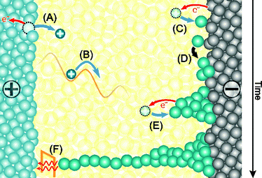 | ||
| Fig. 1 Illustration of the electrochemical processes during SET switching. A positive polarity is applied to the active Ag/Cu electrode. (A) Oxidation of the Ag/Cu active electrode (charge transfer reaction) and dissolution. (B) Migration of Ag/Cu cations under the applied electric field. (C) Reduction reaction at the inert electrode/solid film interface. (D) Nucleation process prior to (E) filamentary growth driven by further reduction processes. (F) When the filament approaches the active electrode significant electron tunneling current sets and the cell switches to a low resistive state. | ||
The nucleation process is related to an activation energy ΔG≠nuc which should be added to the activation energy of the electrode reaction. The formation of the metallic filament on a foreign substrate necessarily starts with a nucleation. The new metal phase can be formed on the counter electrode or within the material, depending on the particular material and experimental conditions. The formed nucleus, which consists of an integer number of metal atoms, has to achieve a critical cluster size of Nc atoms in order to permit further growth. This critical number of atoms depends on the applied voltage and thus, the nucleation contributes to the increase of the reaction overpotential (nucleation overpotential ηnuc). It is thus difficult to formulate an expression for the switching time for a voltage sweep. Therefore, we restrict our study to voltage pulses and the nucleation time tnuc is then given by26,49
 | (1) |
The electron transfer reaction is mathematically described by the Butler–Volmer equation
 | (2) |
 | (3) |
The ion transport within the insulating layer and the corresponding current density can be calculated by the Mott–Gurney law:
 | (4) |
The simulation of the switching kinetics is divided into two steps: nucleation and filamentary growth. First the nucleation time is calculated according to eqn (1). Since the Faradaic currents are zero during nucleation the nucleation overpotential is assumed to be equal to the pulse voltage: ηnuc = Vapp. This approximation is valid as long as the ECM cell is highly insulating in the OFF state and the ionic current dominates. This is true for most ECM systems. When a strong leakage current is present only a part of the applied voltage drives the nucleation. The simulation procedure, however, can still be applied. The cell current during the nucleation is only covered by the electronic contributions. At time tnuc the filamentary growth starts. For the simulation of the filament growth we extend our dynamic switching model42 to cover the nonlinear ionic current transport at high electric fields.
The equivalent circuit diagram of the simulation model is depicted in Fig. 2. The growth is modeled by the change in the tunneling gap between the filament and the active electrode. The cylindrical filament has a lateral area Afil and a resistance Rfil. The dynamic evolution of the tunneling gap is assumed to be one-dimensional and can be mathematically expressed using Faraday's law52
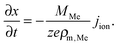 | (5) |
 | (6) |
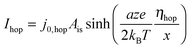
 | (7) |
 | (8) |
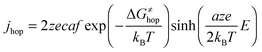
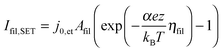
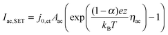
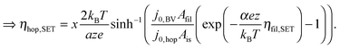
![[thin space (1/6-em)]](https://www.rsc.org/images/entities/char_2009.gif) exp(−G≠hop/kBT). The area Ais has to be considered as equivalent area of ionic conduction within the insulation. The electric field in the insulating layer changes due to the filamentary growth and is given by E = ηhop/x. Hence, the electric field increases with decreasing tunneling gap x and the hopping current increases equivalently. The ionic current density in the ordinary differential equation (eqn (5)) can now be written as a function of one of the overpotentials ηfil, ηac or ηhop. Here, we choose to express eqn (5) as a function of ηfil. Thus, the overpotentials ηac and ηhop need to be rewritten as a function of ηfil. Due to charge neutrality all ionic currents are equal, i.e. Ifil,SET = Iac,SET = Ihop. Combining eqn (6) with eqn (7) and (8), respectively, yields the desired expressions
exp(−G≠hop/kBT). The area Ais has to be considered as equivalent area of ionic conduction within the insulation. The electric field in the insulating layer changes due to the filamentary growth and is given by E = ηhop/x. Hence, the electric field increases with decreasing tunneling gap x and the hopping current increases equivalently. The ionic current density in the ordinary differential equation (eqn (5)) can now be written as a function of one of the overpotentials ηfil, ηac or ηhop. Here, we choose to express eqn (5) as a function of ηfil. Thus, the overpotentials ηac and ηhop need to be rewritten as a function of ηfil. Due to charge neutrality all ionic currents are equal, i.e. Ifil,SET = Iac,SET = Ihop. Combining eqn (6) with eqn (7) and (8), respectively, yields the desired expressions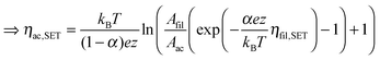 | (9) |
 | (10) |
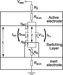 | ||
| Fig. 2 Schematic of the switching model with an equivalent circuit diagram. A switching layer of thickness L is sandwiched between the active top electrode and the inert bottom electrode. A cylindrical filament (the form is arbitrarily chosen for simplicity) grows within the electrolyte film and modulates the tunneling gap x between the filament and the active electrode. In the switching layer both ionic and electronic current paths are present, respectively. | ||
For the RESET process similar expressions for these overpotentials can be derived. As the present study covers only the SET switching kinetics they are not shown here.
As demonstrated in an earlier study the LRS state exhibits a linear I–V characteristic.42 Thus the electron tunneling current equation for the low voltage regime according to Simmons54 is used:
 | (11) |
| Icell = ITu + Iion | (12) |
| Vcell = Icell(Rel + Rs + ρfil(L − x)/Afil) + VTu | (13) |
3. Experimental section
Silver iodide based microcrossbars were fabricated using platinized p-doped (100)-orientated silicon wafers. The Pt bottom electrodes were prepared by UV lithography and subtractive pattern transfer using a Reactive Ion Etching (RIE) tool. Silver iodide is sensitive towards many chemicals (including photoresist developer) and UV light. Thus, once AgI is deposited photolithography cannot be performed without impact on the silver iodide layer. Therefore, the pattern of the top electrodes (overlapping electrode areas between 4 μm2 to 100 μm2) was prepared directly after removal of the bottom electrode photoresist. Subsequently, AgI (Alfa Aesar, purity 99.9% metals basis) layers in the range of 20 nm to 100 nm were deposited into the top electrode pattern by thermal evaporation (0.5 nm s−1) in high vacuum (10−5 mbar) followed by deposition of a 200 nm thick Ag layer by electron-beam (e-beam) evaporation (0.02 nm s−1 at 10−6 mbar). Finally, a lift-off in acetone, isopropanol and deionized water for 5 minutes, respectively, was performed. By making use of this fabrication approach impact of UV light and photoresist developer on AgI can be excluded. Detailed information on the process steps can be found in a previous publication.29For voltage pulse measurements (70 mV ≤ Vapp ≤ 2 V) we used a Wavetek 100 MHz Synthesized Arbitrary Waveform Generator (model 395). Both the transient voltage signal (coupled by 50 Ω input impedance) as well as the current response (coupled by 1 MΩ input impedance) were analyzed using a Tektronix TSD 684A digital oscilloscope (1 GHz bandwidth). The input impedance for the current signal acts additionally as series resistance to limit the current in the low resistive ON state. A triaxial setup (which lowers the effective cable capacity by a factor of 104 to 105) and a radio frequency (RF) shielded screen room have been used for the measurement. We additionally minimized the cable length to measure transient signals within at least 10 ns and ensured by short circuit measurements that RF reflections can be neglected. Note that the OFF resistance (HRS) of AgI microcrossbars is in the range of approximately 200 MΩ. Hence, the voltage drop across the 1 MΩ input impedance during switching can be neglected. For long time voltage pulses (25 mV ≤ Vapp ≤ 100 mV) we used a Keithley 6430 Subfemto-Remote-Source meter. Instead of a series resistor the internal current compliance of the source meter has been set to ICC = 100 nA.
4. Results and discussion
To study the switching kinetics simulations were conducted using the presented ECM model. As excitation voltage pulses with varying amplitude Vapp and a rise time of trise = 5 ns are used. The rise time is chosen according to the experimental setup (short circuit measurements). During the simulation first the nucleation time is calculated according to eqn (1). Afterwards the filament growth is simulated starting at the nucleation time. The switching time tsw is defined as the point in time, where the set current compliance level Icc is reached, i.e. Icc = 100 nA. The used model parameters are given in Table 1.| Symbol | Value | Symbol | Value |
|---|---|---|---|
| M me | 1.79 × 10⁻²² g | ΔG≠nuc | 0.8 eV |
| z | 1 | t 0,nuc | 2 × 10⁻⁸ s |
| ρ m,me | 10.49 g cm−3 | N c | 3 |
| m r | 0.023 | A ac | 804.25 nm2 |
| α | 0.3 | A fil | 12.57 nm2 |
| j 0,et | 3.2 × 10⁵ A m−2 | A is | 12.57 nm2 |
| ΔG≠et | 0.6 eV | L | 20 nm |
| j 0,hop | 1.1 × 10¹¹ A m−2 | ρ fil | 1.7 × 10⁻⁸ Ω m |
| a | 0.25 nm | R el | 76.4 mΩ |
| ΔG≠hop | 0.32 eV | R S | 1 MΩ |
Fig. 3 shows the simulated switching times as a function of the applied voltage for different temperatures T = 298 K, 323 K, 348 K, 373 K compared to the obtained experimental data. Experimental data for T = 298 K and 0.3 V < Vapp < 2 V are extracted from ref. 29. The simulated data are displayed using solid lines and the experimental data using squares. Our simulation model fits perfectly to the experimental data. Moreover, it offers the possibility to analyze the limiting processes during SET switching in different voltage ranges. Here, it can be distinguished between three different regimes (marked I, II, and III). At low voltages Vapp < 0.2 V a very steep slope is observed, which can be related to a nucleation limitation (regime I). Subsequently, the slope becomes flatter up to a voltage range between 0.7 V and 1.2 V (II) at temperatures of 373 K and 298 K, respectively. The third regime (III) appears at even higher voltages and the slope flattens further. In addition, the switching times for the different temperatures seem to converge in the ns regime. The switching times in this time scale, however, are greatly affected by the chosen rise time of 5 ns. Hence, these switching times have to be taken with care while interpreting the data on the switching kinetics.
 | ||
| Fig. 3 Pulsed SET switching kinetics of the AgI-based ECM cell for different ambient temperatures T = 298 K (blue), 323 K (red), 348 K (black) and 373 K (light green). The simulated data are displayed using solid lines and the experimental data using squares. I, II, III mark the nucleation limited, the electron transfer limited and the mixed control regime, respectively. Details of statistical variation can be found in ref. 29. | ||
By analysis of the transient voltages and the transient gaps during switching the limiting factors of the kinetics can be identified. For each of the identified three regimes the transients are evaluated for exemplary voltages of Vapp = 0.15 V, 0.4 V and 2 V.
For the former voltage the nucleation time is tnuc = 2.8 ms and takes up most of the switching time tsw = 3.1 s as illustrated in Fig. 4a. During the nucleation the electron transfer overpotentials ηfil, ηac as well as the hopping overpotential ηhop are zero. Accordingly, the filament does not grow and the tunneling gap remains constant. After nucleation the filament grows comparatively fast until the current compliance is reached. Due to the use of the Tafel equation the calculated filament growth speed is lower compared to the use of the Butler–Volmer equation. In contrast, no nucleation regime is visible in Fig. 4b, but the filamentary growth starts directly. Here, the hopping overpotential is almost zero during switching and the sum of the electron transfer overpotentials ηfil and ηac is equal to the applied voltage. Therefore, the switching kinetics in this regime is limited by the electron transfer reactions occurring at the boundaries. The difference in the overpotentials ηfil and ηac in Fig. 4b is related to the choice of the charge transfer coefficient α = 0.3 and the geometric asymmetry, i.e. Aac > Afil. From this it follows that ηfil > ηac according to eqn (9). Since the electron transfer overpotentials are constant during the voltage pulse, the tunneling gap decreases linearly. In comparison the tunneling gap decreases nonlinearly in the third regime (cf.Fig. 4c). Still, the electron transfer overpotentials account for most of the voltage drop, but they are not constant anymore. This behavior is connected to the occurrence of a hopping overpotential. According to eqn (8)ηhop depends linearly on the tunneling gap. During filamentary growth the tunneling gap and hence the hopping overpotential decrease, while the electron transfer overpotentials in turn increase. Thus, the filament growth becomes nonlinear. When the current compliance sets in, the hopping overpotential is zero and the electron transfer reaction limits the switching speed and prevents the tunneling gap from closing completely. The electron transfer reaction is thus the most relevant process to explain multilevel states by varying tunneling gaps (cf.ref. 42). Without this limitation the tunneling gap would always close since the ionic current increases with decreasing tunneling gap, which would lead to a faster filament growth. As both processes, electron-transfer and hopping transport, play an important role, we call this regime mixed electron-transfer hopping (mixed control) limited regime.
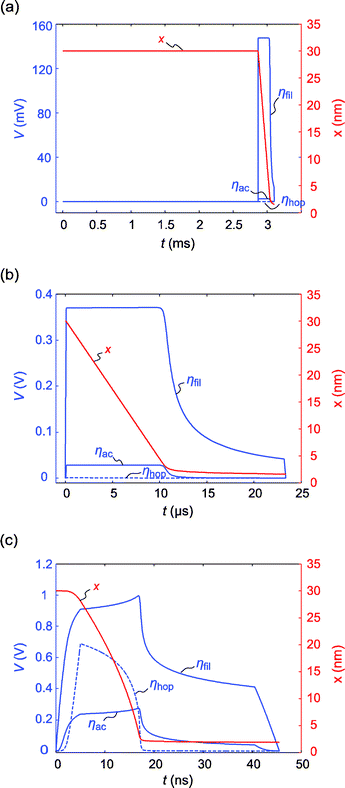 | ||
| Fig. 4 Simulated transient overpotentials (blue) and tunneling gap x (red). The hopping overpotential ηhop is illustrated with blue dashed lines and the electron transfer overpotentials ηfil and ηac with blue solid lines. The transients are shown for an applied voltage of (a) 0.15 V representing the nucleation controlled regime, (b) 0.4 V representing the electron transfer limited regime and (c) 2 V, which corresponds to the mixed control regime. | ||
As mentioned above the finite rise time of the applied voltage pulse can falsify the measurement of the switching kinetics. This effect is also visible in Fig. 4c. Already during the rise time the filament grows a little bit. Thus, the experiment cannot be considered a pure pulse experiment anymore. In order to study the influence of the rise time in more detail, the switching kinetics simulations for T = 298 K were performed at different rise times. As illustrated in Fig. 5 even a rise time of 1 ns influences the resulting switching kinetics whereas the simulation results for trise = 100 ps and 10 ps coincide. In the case of a very long rise time (100 ns) an almost constant switching time matching approximately the rise time results. This means that the whole switching process takes place during the rise time, which is comparable to a sweep experiment rather than a pulse experiment.
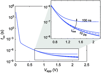 | ||
| Fig. 5 Simulated switching kinetics for varying rise times trise = 10 ps, 100 ps, 1 ns, 5 ns, 10 ns and 100 ns at 298 K. The blue dashed line marks the reference simulation data extracted from Fig. 3 at 298 K. Note that the simulation results for 10 ps and 100 ps coincide. | ||
Up to now we have discussed the switching kinetics with regard to AgI-based ECM cells. In other ECM systems depending on the electrode, electrolyte material and the thermodynamic conditions the electrochemical processes remain the same, but they may be outbalanced differently, thus changing the rate-limiting step. To investigate the switching dynamics of different systems, switching kinetics simulations were performed while varying Nc, t0,nuc, j0,et and j0,hop. Note that the variation of the latter three parameters is equivalent to a change in any parameter determining the constant pre-factors in eqn (1)–(3). The parameters will affect the voltage range of the three regimes, such that a regime might even vanish. Assuming a different critical number of atoms for nucleation leads to a variation of the slope in the nucleation limited regime (cf.Fig. 6a). In agreement with eqn (1) the slope in the switching kinetics plot depends linearly on Nc. Apart from that the nucleation regime broadens for lower Nc. Consequently, the regime limited by the electron transfer kinetics narrows. The variation of the prefactor t0,nuc leads to a parallel shift of the switching kinetics curve in the nucleation limited regime since tsw ∝ t0,nuc holds according to eqn (1). Again, the width of the nucleation limited and in turn the electron transfer limited regimes change as shown in Fig. 6b. The results of this simulation study offer the opportunity to explain an occurring electroforming cycle in ECM cells. In contrast to AgI, in some ECM cells (e.g. for SiO216 or Ta2O514) the first switching voltage is higher (the initial electroforming cycle) than in the successive SET cycles. This has been attributed to the formation of preferred ionic paths in the insulating layer, which is accompanied by mechanical stress.47 Alternatively, the higher forming voltage can be explained by additional strain energy accounting for necessarily breaking of electrode–electrolyte bonding in order to form the critical nucleus.25 Hence, an additional energy barrier has to be overcome. Both effects were unified and modeled by multiplication of an additional activation energy term exp(ΔG≠form/kBT) according to eqn (1), which is equivalent to an increase of t0,nuc. So for the initial cycle the switching kinetics curve would be shifted to slower switching times and the switching voltage is increased. In the following cycles the multiplication factor is 1 and Vsw is lower.
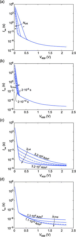 | ||
| Fig. 6 Parameter variation study of the switching kinetics. The blue dashed lines mark the reference simulation data extracted from Fig. 3 at 298 K. (a) Variation of the critical amount of atoms for nucleation Ncrit = 1, 2, 3, and 4. (b) Variation of the nucleation prefactor t0,nuc = 2 × 10⁻⁶ s, 2 × 10⁻⁷ s, 2 × 10⁻⁸ s, 2 × 10⁻⁹ s, and 2 × 10⁻¹⁰ s. (c) Variation of the exchange current density j0,et = 3.2 × 10³ A m−2, 3.2 × 10⁴ A m−2, 3.2 × 10⁵ A m−2, 3.2 × 10⁶ A m−2, and 3.2 × 10⁷ A m−2. (d) Variation of j0,hop = 1.1 × 10⁹ A m−2, 1.1 × 10¹⁰ A m−2, 1.1 × 10¹¹ A m−2, 1.1 × 10¹² A m−2, and 1.1 × 10¹³ A m−2. | ||
In Fig. 6c the influence of the exchange current density on the switching kinetics is illustrated. Due to the linear dependence of the ionic current on the exchange current density the switching time is inversely proportional according to tsw ∝ j0,et−1. With lower exchange current density the electron transfer limited regime broadens whereas it narrows for higher exchange current densities. For j0,et = 3.2 × 10⁷ A m−2 the electron transfer regime almost vanishes. By varying j0,hop the switching time in the mixed regime is varied as shown in Fig. 6d. Similarly to the variation of j0,et, tsw ∝ j0,hop−1 holds. This dependence, however, is superimposed by the influence of the rise time if j0,hop > 1.1 × 10¹¹ A m−2. For lower values of j0,hop the mixed regime extends more into the electron transfer regime, which might finally become not observable. It should be noted that a variation of the charge transfer coefficient α would lead to variation of the slope in the electron transfer limited as well as the nucleation limited regime according to eqn (1)–(3) in analogy to the change in Nc. Equivalently, it is supposed that changing the hopping distance a or the charge number z will lead to variation of the slope in the mixed regime. But this could not be clearly observed in simulations due to complex interaction between the limiting process (electron transfer) and ion hopping transport. In addition, the finite rise time again influences the switching kinetics in the corresponding time regime. This limitation may eventually mask the limiting physically process, which allows faster switching times.
5. Conclusions
We presented an advanced model for the switching kinetics of ECM cells accounting for all relevant rate limiting processes under variable experimental conditions. The model was exemplarily applied to AgI-based ECM cells showing a full compatibility of theoretical and experimental data. Based on our results we conclude the following:(1) The analysis of the simulation data revealed the presence of three different regimes in the switching kinetics of AgI-based ECM cells: the nucleation limited regime, the electron transfer limited regime and the mixed electron transfer ion hopping limited regime.
(2) The influence of the physical parameters on the switching kinetics has been critically discussed. Depending on the parameter values the processes limiting the switching kinetics change. As a result the voltage ranges of the regimes might vary or even less than three regimes might be observed in experiment.
(3) Based on the simulation results a possible explanation for the electroforming event was presented. The formation of preferred ionic paths in the insulating layer accompanied by mechanical stress or additional strain energy accounting for necessarily breaking of electrode–electrolyte bonding in order to form the critical nucleus results in an additional energy barrier that has to be overcome. This results in an increased switching voltage for the initial electroforming cycle.
(4) The analyses of the time-dependent overpotentials revealed that the electron transfer reaction limits the kinetics when the current compliance is reached. The electron transfer reaction is thus the most relevant process to explain multilevel states by varying tunneling gaps.
(5) It is shown that the measurement setup, e.g. a finite rise time, can influence the switching kinetics dramatically at corresponding switching times. Thus, analyses of the experimental data in this regime assuming a pure pulse experiment lead to a misinterpretation.
This demonstrates the wide applicability of the derived switching model.
Acknowledgements
The authors would like to thank P. Roegels for preparing thermally evaporated AgI thin films and J. Müller for code development. This work was supported in part by the Samsung Global Research Outreach Program.Notes and references
-
Nanoelectronics and Information Technology, ed. R. Waser, Wiley-VCH, 3rd edn, 2012 Search PubMed
.
- Y. Fujisaki, Jpn. J. Appl. Phys., 2010, 49, 100001 CrossRef
- C. Kügeler, R. Rosezin, R. Weng, S. Menzel, B. Klopstra, U. Böttger and R. Waser, Proceedings of the 9th IEEE Conference on Nanotechnology, 900, 2009.
- R. Rosezin, E. Linn, L. Nielen, C. Kügeler, R. Bruchhaus and R. Waser, IEEE Electron Device Lett., 2011, 32, 191 CrossRef CAS
- J. Borghetti, G. S. Snider, P. J. Kuekes, J. J. Yang, D. R. Stewart and R. S. Williams, Nature, 2010, 464, 873 CrossRef CAS
- E. Linn, R. Rosezin, S. Tappertzhofen, U. Böttger and R. Waser, Nanotechnology, 2012, 23, 305205 CrossRef CAS
- T. Ohno, T. Hasegawa, T. Tsuruoka, K. Terabe, J. K. Gimzewski and M. Aono, Nat. Mater., 2011, 10, 591 CrossRef CAS
- R. Waser and M. Aono, Nat. Mater., 2007, 6, 833 CrossRef CAS
- U. Russo, D. Kamalanathan, D. Ielmini, A. L. Lacaita and M. N. Kozicki, IEEE Trans. Electron Devices, 2009, 56, 1040 CrossRef CAS
- K. Terabe, T. Hasegawa, T. Nakayama and M. Aono, Nature, 2005, 433, 47 CrossRef CAS
- I. Valov and M. N. Kozicki, J. Phys. D: Appl. Phys., 2013, 46, 074005 CrossRef CAS
- T. Tsuruoka, T. Hasegawa, K. Terabe and M. Aono, Nanotechnology, 2012, 23, 435705 CrossRef
- L. Yang, C. Kügeler, K. Szot, A. Rüdiger and R. Waser, Appl. Phys. Lett., 2009, 95, 13109 CrossRef
- T. Tsuruoka, K. Terabe, T. Hasegawa, I. Valov, R. Waser and M. Aono, Adv. Funct. Mater., 2012, 22, 70 CrossRef CAS
- M. N. Kozicki, M. Park and M. Mitkova, IEEE Trans. Nanotechnol., 2005, 4, 331 CrossRef
- Y. Bernard, V. T. Renard, P. Gonon and V. Jousseaume, Microelectron. Eng., 2011, 88, 814 CrossRef CAS
- T. Hasegawa, K. Terabe, T. Tsuruoka and M. Aono, Adv. Mater., 2012, 24, 252 CrossRef CAS
- D.-Y. Cho, I. Valov, J. van den Hurk, S. Tappertzhofen and R. Waser, Adv. Mater., 2012, 24, 4552 CrossRef CAS
- C. Schindler, I. Valov and R. Waser, Phys. Chem. Chem. Phys., 2009, 11, 5974 RSC
- D.-Y. Cho, S. Tappertzhofen, R. Waser and I. Valov, Sci. Rep., 2013, 3, 1169 Search PubMed
- A. Nayak, T. Tsuruoka, K. Terabe, T. Hasegawa and M. Aono, Nanotechnology, 2011, 22, 235201 CrossRef
- A. Nayak, T. Tamura, T. Tsuruoka, K. Terabe, S. Hosaka, T. Hasegawa and M. Aono, J. Phys. Chem. Lett., 2010, 1, 604 CrossRef CAS
- S. Tappertzhofen, H. Mündelein, I. Valov and R. Waser, Nanoscale, 2012, 4, 3040 RSC
- S. Tappertzhofen, S. Menzel, I. Valov and R. Waser, Appl. Phys. Lett., 2011, 99, 203103 CrossRef
- I. Valov and G. Staikov, J. Solid State Electrochem., 2013, 17, 365 CrossRef CAS
- R. Soni, P. Meuffels, G. Staikov, R. Weng, C. Kuegeler, A. Petraru, M. Hambe, R. Waser and H. Kohlstedt, J. Appl. Phys., 2011, 110, 54509 CrossRef
- T. Tsuruoka, K. Terabe, T. Hasegawa and M. Aono, Nanotechnology, 2010, 21, 425205 CrossRef CAS
- T. Tsuruoka, K. Terabe, T. Hasegawa and M. Aono, Nanotechnology, 2011, 22, 254013 CrossRef
- S. Tappertzhofen, I. Valov and R. Waser, Nanotechnology, 2012, 23, 145703 CrossRef CAS
- Y. Yang, P. Gao, S. Gaba, T. Chang, X. Pan and W. Lu, Nat. Commun., 2012, 3, 732 CrossRef
- Q. Liu, S. Long, H. Lv, W. Wang, J. Niu, Z. Huo, J. Chen and M. Liu, ACS Nano, 2010, 4, 6162 CrossRef CAS
- Z. Xu, Y. Bando, W. Wang, X. Bai and D. Golberg, ACS Nano, 2010, 4, 2515 CrossRef CAS
- J. J. T. Wagenaar, M. Morales-Masis and J. M. van Ruitenbeek, J. Appl. Phys., 2012, 111, 14302 CrossRef
- J. R. Jameson, N. Gilbert, F. Koushan, J. Saenz, J. Wang, S. Hollmer, M. Kozicki and N. Derhacobian, IEEE Electron Device Lett., 2012, 33, 257 CrossRef CAS
- M. Morales-Masis, H. Wiemhofer and J. M. van Ruitenbeek, Nanoscale, 2010, 2, 2275 RSC
- D.-Y. Cho, S. Tappertzhofen, R. Waser and I. Valov, Nanoscale, 2013, 5, 1781–1784 RSC
- S. Menzel, B. Klopstra, C. Kügeler, U. Böttger, G. Staikov and R. Waser, Mater. Res. Soc. Symp. Proc., 2009, 1160, 101 CrossRef
- F. Pan, S. Yin and V. Subramanian, IEEE Electron Device Lett., 2011, 1 Search PubMed
- V. V. Zhirnov, R. Meade, R. K. Cavin and G. Sandhu, Nanotechnology, 2011, 22, 254027 CrossRef
- J. R. Jameson, N. Gilbert, F. Koushan, J. Saenz, J. Wang, S. Hollmer and M. Kozicki, Appl. Phys. Lett., 2012, 100, 23505 CrossRef
- S. Lin, L. Zhao, J. Zhang, H. Wu, Y. Wang, H. Qian and Z. Yu, 2011 IEEE International Electron Devices Meeting – IEDM '12, 2012.
- S. Menzel, U. Böttger and R. Waser, J. Appl. Phys., 2012, 111, 014501 CrossRef
-
S. Choi, S. Ambrogio, S. Balatti, F. Nardi and D. Ielmini, Memory Workshop (IMW), 2012 4th IEEE International, 2012, pp. 1–4 Search PubMed
- I. Valov, I. Sapezanskaia, A. Nayak, T. Tsuruoka, T. Bredow, T. Hasegawa, G. Staikov, M. Aono and R. Waser, Nat. Mater., 2012, 11, 530 CrossRef CAS
- S. Yu and H.-S. Wong, IEEE Trans. Electron Devices, 2011, 58, 1352 CrossRef CAS
- J. R. Jameson, N. Gilbert, F. Koushan, J. Saenz, J. Wang, S. Hollmer and M. N. Kozicki, Appl. Phys. Lett., 2011, 99, 063506 CrossRef
- I. Valov, R. Waser, J. R. Jameson and M. N. Kozicki, Nanotechnology, 2011, 22, 254003 CrossRef
- C. Schindler, G. Staikov and R. Waser, Appl. Phys. Lett., 2009, 94, 072109 CrossRef
-
E. Budevski, G. Staikov and W. J. Lorenz, Electrochemical Phase Formation and Growth, VCH, 1996 Search PubMed
- P. Meuffels and H. Schroeder, Appl. Phys. A: Mater. Sci. Process., 2011, 105, 65 CrossRef CAS
-
J. J. O'Dwyer, The Theory of Electrical Conduction and Breakdown in Solid Dielectrics, Clarendon Press, Oxford, 1973 Search PubMed
- M. Faraday, Philos. Trans. R. Soc. London, 1834, 124, 77 CrossRef
-
C. H. Hamann, A. Hamnett and W. Vielstich, Electrochemistry, Wiley-VCH, Weinheim, 2007 Search PubMed
- J. G. Simmons, J. Appl. Phys., 1963, 34, 1793 CrossRef
| This journal is © the Owner Societies 2013 |