Low variability with high performance in thin-film transistors of semiconducting carbon nanotubes achieved by shortening tube lengths
Shigekazu
Ohmori
a,
Kazuki
Ihara
bc,
Fumiyuki
Nihey
bc,
Yuki
Kuwahara
ab and
Takeshi
Saito
*ab
aNanotube Research Center, National Institute of Advanced Industrial Science and Technology, Tsukuba, Ibaraki, 305-8565, Japan. E-mail: takeshi-saito@aist.go.jp; Fax: +81-29-861-4413; Tel: +81-29-861-4863
bTechnology Research Association for Single Wall Carbon Nanotubes, Tsukuba, Ibaraki, 305-8565, Japan
cNEC Smart Energy Research Laboratories, Tsukuba, Ibaraki, 305-8501, Japan
First published on 12th October 2012
Abstract
Extremely low variability with excellent device performances in a SWCNT-TFT array has been demonstrated in SWCNT-TFTs fabricated by using a semiconducting ink of short SWCNTs with an average length of 340 nm; the field-effect mobility of 3.9 ± 0.45 cm2 V−1 s−1, on/off ratio from 105 to 106, and hysteresis of ≈0.5 V. AFM observations revealed that the nonionic surfactant, Brij 700, adopted for dispersing SWCNTs during their extraction, causes the significant and homogeneous shortening of SWCNTs compared with sodium cholate, which is frequently used for the dispersion of SWCNTs as an ionic surfactant. Thus, it has been concluded that the shortening of SWCNTs in the dispersing process using the Brij 700 surfactant contributes to the observed uniformity of performance among the devices.
Introduction
Single-wall carbon nanotubes (SWCNTs) have attracted considerable attention as a potential semiconducting material1 in the ink applied to “printed electronics”2 because of their excellent electronic properties, as well as their flexibility and chemical robustness.3 For the printed electronics of SWCNTs, various processes, not only the printing process itself, but also the semiconducting-ink preparation and removal of surfactants by heat and/or wet treatments, are required.4 Among these processes, recent significant advances in the extraction techniques for the ink preparation of semiconducting SWCNTs (s-SWCNTs), such as dielectrophoresis,5 density-gradient ultracentrifugation,6 DNA separation,7 and gel-based extraction8 have improved the device performance of thin-film transistors of SWCNTs (SWCNT-TFTs). Although most of the reported extraction methods need to use ionic surfactants to disperse SWCNTs, it is well known that ionic contaminations can degrade device performance.9,10 Therefore using ionic surfactants in the extraction process should be avoided to allow more significant improvements in SWCNT-TFTs. Recently, the electric-field-induced layer formation (ELF) method,11 which adopts a nonionic surfactant, have demonstrated the high purity of s-SWCNTs of up to 95% with excellent transport properties in SWCNT-TFTs.Besides the purity of s-SWCNTs, many geometrical parameters, such as the most basic parameters of tube length12 and diameter,13 can directly affect the device characteristics. In particular, the effect of the tube length is complicated because it influences SWCNT-TFTs in terms of some different aspects of device performance. For example, it was reported that long SWCNTs lead to a prominent high-mobility above 100 cm2 V−1 s−1 due to the reduction in the number of contacts and their resistance.14,15 In contrast, a simulation study predicted that SWCNTs much shorter than the channel length of devices can contribute to a decrease in the error probability in the device performance, which results in the improvement of device reliability.16 Accordingly, it is important to characterize the tube length distribution in the SWCNT dispersion for the analysis of SWCNT-TFT performance. A printed SWCNT-TFT array with low variability in the device performances will be applicable for a large-area, low-cost, and flat-panel sensor.
Here we have fabricated SWCNT-TFTs by using a dispersion of s-SWCNTs separated by the ELF method11 as a novel semiconducting ink of SWCNTs not containing ionic surfactants. The transfer and output characteristics of SWCNT-TFTs have been measured and statistically analyzed on the basis of the lengths of the SWCNTs as characterized by atomic force microscopy (AFM) observation.
Experimental
The SWCNTs used in this study were synthesized by gas-phase CVD growth using the enhanced direct-injection pyrolytic synthesis (eDIPS) method.17 For the SWCNTs with a 1.3 nm diameter, the extraction of the s-SWCNT fraction was carried out based on the electric-field-induced layer formation (ELF) technique,11 which is an electrophoresis method. Semiconducting chiralities in the used SWCNTs observed by the photoluminescence mapping measurement (Horiba Spex, Fluorolog 3-2 TRIAX) were as follows: (8,6), (8,7), (9,7), (9,8), (10,5), (10,6), (10,8), (10,9), (11,3), (11,4), (11,6), (11,7), (11,9), (12,1), (12,4), (12,5), (12,7), (12,8), (13,2), (13,3), (13,5), (13,6), (14,1), and (14,3). The purity of the s-SWCNT fraction was measured to be 97% by the optical absorption (Hitachi, U-4000) and Raman scattering (Horiba Jobin Yvon, HR-800) spectroscopy measurements.The s-SWCNT thin film was deposited on heavily doped silicon substrates (Sb doped, 0.02 Ω cm) covered by a 100 nm-thick SiO2 layer serving as a gate dielectric. The surface of the substrate was cleaned by oxygen plasma (PR500: Yamato Scientific Co., Ltd.) with a power of 300 W for 180 s and was functionalized by aminopropyltriethoxysilane (Wako) prior to nanotube deposition. Such amino-functionalization increases the adsorption of SWCNTs on the substrate, and reduces the contribution to the hysteresis due to fixed charges on the substrate surface.18–21 Subsequently, the amino-functionalized substrate was immersed into the s-SWCNTs dispersion for 1 h. The morphology of the deposited SWCNTs was observed by AFM (Seiko SPM-400). Amino-functionalization and s-SWCNT deposition were repeated as needed for increasing the density of SWCNTs. The deposited s-SWCNT thin film on the substrate was washed with water and 2-propanol. Then the substrates were annealed at 170 °C for 30 min in air. Au electrodes (thickness: 100 nm) were deposited by evaporation of the s-SWCNT thin film on the substrate through a patterned shadow mask for fabricating TFT devices. Each channel of the TFT devices was then masked by poly-methylmethacrylate (PMMA). After the masking, redundant s-SWCNTs were removed by oxygen plasma. Thereby, a TFT device array with a channel width of 500 μm and three different channel lengths of 50, 100, and 200 μm was fabricated.
The device performance of assembled SWCNT-TFTs was measured by using a semi-automatic probe station (Cascade Summit 12![[thin space (1/6-em)]](https://www.rsc.org/images/entities/char_2009.gif) 000) and a semiconductor parameter analyser (Agilent 4156C). A drain–source voltage of −1 V was applied for the measurement of the transfer characteristics with gate voltages ranging from −10 V to +10 V. The output characteristics were measured by sweeping a drain-source voltage from 0 V to −10 V at gate voltages ranging from −10 V to +10 V in 2 V steps.
000) and a semiconductor parameter analyser (Agilent 4156C). A drain–source voltage of −1 V was applied for the measurement of the transfer characteristics with gate voltages ranging from −10 V to +10 V. The output characteristics were measured by sweeping a drain-source voltage from 0 V to −10 V at gate voltages ranging from −10 V to +10 V in 2 V steps.
In order to perform a comparison study of the resulting length distributions, SWCNT dispersions with two different surfactants were prepared in the following manner; 1 mg of SWCNTs was dispersed into 20 ml of aqueous solutions of 1 wt% sodium cholate (Wako), or polyoxyethylene (100) stearyl ether (Brij 700, Aldrich) with the help of pulsed sonication (on: 1 s, off: 2 s) applied with a power of 200 W for 0.5 h by using a tip ultrasonic homogenizer (SONICS VCX500) equipped with a titanium alloy tip (TI-6AL-4V). The dispersion of SWCNTs was then centrifuged at 127600g (Hitachi CP100MX with a P56ST swing rotor) to precipitate large bundled SWCNTs.
For characterization of the length distribution of SWCNTs by AFM, specimens were prepared by the following procedure: the SWCNT dispersion was dropped on the amino-functionalized Si substrates and washed with water to remove the detergents. This procedure was repeated until the density of SWCNTs became suitable in the AFM image for the investigation of their length distribution. The lengths of more than 1000 individual SWCNTs were counted in order to make a length distribution histogram with 100 nm binning.
Results and discussion
Fig. 1a shows the typical transfer and output characteristics of p-type SWCNT-TFTs. The n-type transfer characteristics were also observed for VGS > 0 V in the logarithmic-scale transfer characteristics, which clearly demonstrate the ambipolar nature of s-SWCNTs. The output characteristic plotted in the inset of Fig. 1a shows the saturation behavior of the drain current at large VDS, which is interpreted as the absence of metallic pathways in the semiconducting channel due to the sufficient purity of the s-SWCNTs in the semiconducting ink. The threshold voltage (Vth) estimated by the extrapolation of the linear region to zero drain current is lower than 0 V, suggesting that the fabricated SWCNT-TFTs are intrinsically an enhancement-type, although a small amount of drain current still remains at VGS = 0 V because of the slow variation of the drain current in the sub-threshold region. It should be noted that all fabricated devices have very similar profiles with low variability, suggesting that the s-SWCNTs and their deposited network are extremely uniform as discussed below.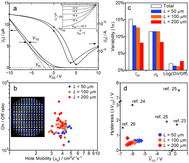 | ||
| Fig. 1 Device properties of SWCNT-TFTs. a) Typical transfer and output (inset) characteristics. b) On/off ratio as a function of the field-effect mobility. c) Variabilities (1σ) of the on-current, field-effect mobility, and on/off ratio in SWCNT-TFTs fabricated on one substrate. d) Hysteresis in terms of the gate voltage for the drain current equal to half of the on-current value (V1/2). The difference of V1/2 between forward and reverse sweeps is plotted against the average; some other reported values23–26 are included for comparison. | ||
The on/off ratios are plotted against the field-effect mobilities for a total of 60 devices fabricated on one substrate (20 devices for each of the channel lengths L = 50, 100, and 200 μm) in Fig. 1b. The mobility derived from the maximum transconductance was calculated using a simple parallel plate mode. Fig. 1b shows that these devices have high performance with extremely low variability; the field-effect mobility is 3.9 ± 0.45 cm2 V−1 s−1, and the on/off ratio is distributed within one order of magnitude between 105 and 106. These device characteristics would guarantee the excellent homogeneity of the deposited SWCNT network in addition to the above-mentioned high purity of the s-SWCNT ink extracted by ELF. The other characteristics are also listed in Table 1.
| Total (60 devices) | L = 50 μm (20 devices) | L = 100 μm (20 devices) | L = 200 μm (20devices) | ||
|---|---|---|---|---|---|
| I on(p) (μA) | — | 11.5 ± 1.5 | 5.10 ± 0.47 | 2.29 ± 0.19 | |
| I on(p)(L W−1) (μA) | 1.03 ± 0.16 | 1.15 ± 0.15 | 1.02 ± 0.13 | 0.92 ± 0.08 | |
| m p (cm2 V−1 s−1) | 3.93 ± 0.45 | 4.16 ± 0.48 | 3.90 ± 0.45 | 3.72 ± 0.31 | |
| On/Off ratio | 105.35 ± 0.10 | 105.30 ± 0.070 | 105.35 ± 0.062 | 105.39 ± 0.15 | |
| I on(n) (nA) | 3.35 ± 1.4 | 3.35 ± 1.4 | 3.40 ± 1.1 | 3.60 ± 1.1 | |
| I off (pA) | Forward | 24.2 ± 20 | 49.4 ± 10 | 17.5 ± 3.7 | 5.65 ± 3.2 |
| Backward | 38.7 ± 23 | 67.9 ±13 | 30.2 ± 3.8 | 18.2 ± 3.2 | |
| V(Ioff) (V) | Forward | 4.58 ± 0.65 | 5.19 ± 0.67 | 4.52 ± 0.29 | 4.02 ± 0.21 |
| Backward | 3.41 ± 0.65 | 3.96 ± 0.80 | 3.34 ± 0.24 | 2.92 ± 0.20 | |
| V th (V) | Forward | −0.16 ± 0.6 | −1.02 ± 0.56 | −1.66 ± 0.30 | −2.12 ± 0.24 |
| Backward | −2.56 ± 0.51 | −2.12 ± 0.54 | −2.58 ± 0.25 | −2.97 ± 0.23 | |
| G mmax (μS) | Forward | — | 1.31 ± 0.16 | 0.62 ±0. 07 | 0.29 ± 0.02 |
| Backward | — | 1.57 ± 0.18 | 0.73 ± 0.09 | 0.35 ± 0.03 | |
In order to discuss the variability of the performance across many devices quantitatively, the standard deviations (1σ) of the on-current, mobility, and the common logarithm of the on/off ratio (log10(On/Off)) have been analyzed, as shown in Fig. 1c. The extremely low deviation (1σ < 15%) relative to previously reported values for SWCNT-TFTs15,22 supports the remarkable homogeneity of device characteristics in the present work.
Interestingly, the variation of the on-current and mobility diminishes with increasing channel length L, which is due to the effect of averaging the network connectivity. On the other hand, the variation of the on/off ratio represents the opposite trend, which is mainly ascribable to the increasing off-current variation with increasing L. More specifically, with regard to the measurement of the relatively low off-current around 10−12 A at L = 200 μm, the variation of the on/off ratio can be explained by the effect of the capacitance current on the off-current.
To date, a relatively large hysteresis in the output and transfer characteristics was a serious problem in SWCNT-TFTs.23 Although previous reports reduced the contribution to the hysteresis due to fixed charges on the substrate surface by coating the oxide with a hydrophobic self-assembled monolayer (SAM) as performed in the present work,18–21 the effect of surfactants on the hysteresis8 is still critical in SWCNT-TFTs fabricated by using dispersions. For characterizing the hysteresis, the gate voltages were analyzed at a drain current equal to half of the on-current value in the p-type characteristics, which are specified as V1/2. In Fig. 1d, the hysteresis, expressed as the difference of V1/2 between the forward and reverse sweeps (denoted by ΔV1/2 in Fig. 1a), is plotted against the average value ((V1/2forward + V1/2reverse)/2). Fig. 1d appears to show a significant improvement of the hysteresis problem in the present work compared with recent works.23–26 In addition, Fig. 1d shows a clear correlation between V1/2 and the hysteresis that depends on the channel length L. Such channel-length dependence could be interpreted as the decreasing influence of charge transfer from gold electrodes to the SWCNT channel near their interface.27
As reported in the recent simulation study on the SWCNT-TFTs with the random network channel,16 the variability of device characteristics should be essentially attributed to the effect of the SWCNT length; i.e., the uniformity of device performances can be achieved by shortening the lengths of the SWCNTs. Therefore, the tube length distribution in the s-SWCNT ink has been characterized by AFM measurement to investigate the influence of tube length on the variability of device performances.
Fig. 2a shows the AFM image of well-isolated s-SWCNTs used for fabricating SWCNT-TFTs in the present work. The height information distributed around 1–3 nm suggests that individual SWCNTs with a small quantity of narrow-bundled SWCNTs are deposited on the sample substrate. The histogram of the s-SWCNT length, plotted in Fig. 2b, was obtained by measuring length values of more than 1000 SWCNTs. The lengths of the s-SWCNTs are mainly distributed over less than 1 μm, with an average length of 340 nm. The observed SWCNTs are sufficiently shorter than the channel length L, which will contribute to the high-level of uniformity observed in the performance of the devices, as theoretically predicted. The shape of the histogram agrees well with the log-normal distribution, suggesting that the statistical effect determines the shape of the length distribution.
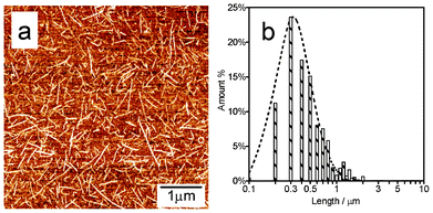 | ||
| Fig. 2 Statistical analysis of tube length in s-SWCNTs ink based on AFM observations. a) A typical AFM image of s-SWCNTs mono-dispersed on silicon substrate. b) A length distribution chart, representing the distribution of the total length of all the tubes into different length ranges, measured from AFM images of s-SWCNTs. The vertical axis displays the sum of the lengths of all the tubes in each bin normalized by the total length of all measured s-SWCNTs. | ||
To verify the process that shortens the tube lengths in s-SWCNTs extracted by ELF, we have analyzed the tube lengths of two different SWCNT samples, one being dispersed by using Brij 700 as the surfactant in ELF, and the other by sodium cholate (SC), which is frequently used as a general surfactant; these dispersions were both carried out through the same procedure using a tip homogenizer and ultracentrifugation. (For detailed descriptions of the procedures, see the Experimental section.)
The length distribution histograms of both the SC- and Brij-dispersion samples are shown in Fig. 3a and 3b, respectively. As with the length distribution of the s-SWCNTs shown in Fig. 2b, the shape of the histograms for each of these samples agrees well with the log-normal distribution. Interestingly, the length value at the peak of the histogram for the Brij-dispersion (Fig. 3b) is definitely shorter than that of the SC-dispersion (Fig. 3a). Furthermore, the length distribution of the Brij-dispersion is narrower. In other words, the length distribution of the Brij-dispersion is weighted toward the shorter end of the length range than the SC-dispersion. The average lengths of the SC- and Brij-dispersions calculated from their length distributions are 520 and 360 nm, respectively. These results clearly suggest that the dispersing process using Brij 700 shortens the SWCNTs and produces a greater homogeneity in their length that contributes to the above-mentioned uniformity of device performances. In Fig. 4, the average lengths of the SC- and Brij-dispersions have been plotted for SWCNT samples with different mean diameters, 0.9, 1.3, and 2.1 nm. In the case of the SC-dispersions, an obvious dependence of the average length on the diameter is found, i.e., the average length monotonically becomes longer with increasing diameter. In contrast, the average lengths of the Brij-dispersions, appearing at around 300–400 nm, show less dependence on the diameter of the SWCNTs. In particular, the observed difference in the average length of the SWCNTs is pronounced with an increase in the diameter. Because the shortening of SWCNTs in their dispersion process can be triggered by the chemical reaction forming epoxy groups,28 the observed difference of the tube length between the SC- and Brij-dispersions might originate from the difference in the proportion of oxygen atoms in the molecular structures of these surfactants. Although considerable work reporting the difference in the dispersing ability of SWCNTs among various surfactants has been carried out,29,30 this result has clarified for the first time that the different surfactants influence not only the dispersing state but also the length of the SWCNTs.
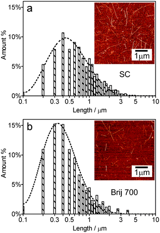 | ||
| Fig. 3 Length distribution charts of two different SWCNT samples, accompanied by typical AFM images for the samples in the insets. The SWCNTs are dispersed by using a) sodium cholate (SC) and b) the Brij 700 used in the preparation of our s-SWCNT ink. | ||
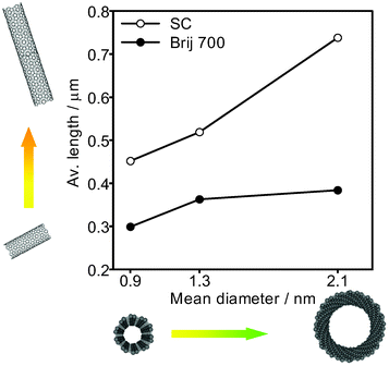 | ||
| Fig. 4 Average length of SWCNTs dispersed by using SC (open circles) and Brij 700 (filled circles) for the characterization of diameter dependences in the shortening effect of the dispersing process. The mean diameters were determined by using the reported method.31 | ||
Conclusions
We have fabricated SWCNT-TFTs by using a novel semiconducting ink of SWCNTs without contamination with ionic surfactants in order to investigate their transport properties. Statistical analysis of the transfer and output characteristics of the SWCNT-TFTs has demonstrated the extremely low variability in the excellent performances of the devices: the field-effect mobility of 3.9 ± 0.45 cm2 V−1 s−1 and the on/off ratio between 105 and 106. On the basis of the lengths of the SWCNTs characterized by AFM observations, it has been concluded that the shortening of SWCNTs in the dispersing process using the Brij 700 surfactant contributes to the observed uniformity of performance among the devices.Acknowledgements
This work has been supported by the New Energy and Industrial Technology Development Organization (NEDO). T. S. would like to thank Dr T. Okazaki and Dr M. Tange for their experimental help.References
- Q. Cao and J. A. Rogers, Adv. Mater., 2009, 21, 29 CrossRef CAS.
- N. Rouhi, D. Jain, K. Zand and P. J. Burke, Adv. Mater., 2011, 23, 94 CrossRef CAS.
- Carbon Nanotubes: Synthesis, Structure, Properties, and Applications, Springer: Berlin, New York, 2001 Search PubMed.
- H. Numata, K. Ihara, T. Saito and F. Nihey, Appl. Phys. Express, 2012, 5, 055102 CrossRef.
- R. Krupke, F. Hennrich, H. Löhneysen and M. M. Kappes, Science, 2003, 301, 344 CrossRef CAS.
- M. S. Arnold, A. A. Green, J. F. Hulvat, S. I. Syupp and M. C. Hersam, Nat. Nanotechnol., 2006, 1, 60 CrossRef CAS.
- M. Zheng, A. Jagota, E. D. Semke, B. A. Diner, R. S. McLean, S. R. Lustig, R. E. Richardson and N. G. Tassi, Nat. Mater., 2003, 2, 338 CrossRef CAS.
- T. Tanaka, H. Jin, Y. Miyata, S. Fujii, H. Suga, Y. Naitoh, T. Minari, T. Miyadera, K. Tsukagoshi and H. Kataura, Nano Lett., 2009, 9, 1497 CrossRef CAS.
- C.-J. Shih, G. L. C. Paulus, Q. H. Wang, Z. Jin, D. Blankschtein and M. S. Strano, Langmuir, 2012, 28, 8579 CrossRef CAS.
- K. Bradley, J. Cumings, A. Star, J.-C. P. Gabriel and G. Grüner, Nano Lett., 2003, 3, 639 CrossRef CAS.
- K. Ihara, H. Endoh, T. Saito and F. Nihey, J. Phys. Chem. C, 2011, 115, 22827 CAS.
- Y. Asada, Y. Miyata, K. Shiozawa, Y. Ohno, R. Kitaura, T. Mizutani and H. Shinohara, J. Phys. Chem. C, 2010, 115, 270 Search PubMed.
- Y. Asada, S. Ohmori, F. Nihey, H. Shinohara and T. Saito, Adv. Mater., 2011, 23, 4631 CrossRef CAS.
- Y. Miyata, K. Shiozawa, Y. Asada, Y. Ohno, R. Kitaura, T. Mizutani and H. Shinohara, Nano Res., 2011, 4, 963 CrossRef CAS.
- D. Sun, M. Y. Timmermans, Y. Tian, A. G. Nasibulin, E. I. Kauppinen, S. Kishimoto, T. Mizutani and Y. Ohno, Nat. Nanotechnol., 2011, 6, 156 CrossRef CAS.
- M. Ishida and F. Nihey, Appl. Phys. Lett., 2008, 92, 163507 CrossRef.
- T. Saito, S. Ohshima, T. Okazaki, S. Ohmori, M. Yumura and S. Iijima, J. Nanosci. Nanotechnol., 2008, 8, 6153 CrossRef CAS.
- G. S. Duesberg, J. Muster, V. Krstic, M. Krstic, M. Burghard and S. Roth, Appl. Phys. A: Mater. Sci. Process., 1998, 67, 117 CrossRef CAS.
- A. D. Franklin, G. S. Tulevski, S.-J. Han, D. Shahrjerdi, Q. Cao, H-Y. Chen, H.-S. P. Wong and W. Haensch, ACS Nano, 2012, 6, 1109 CrossRef CAS.
- S. A. McGill, S. G. Rao, P. Manandhar, P. Xiong and S. Hong, Appl. Phys. Lett., 2006, 89, 163123 CrossRef.
- P. Hu, C. Zhang, A. Fasoli, V. Scardaci, S. Pisana, T. Hasan, J. Robertson, W. I. Milne and A. C. Ferrari, Phys. E., 2008, 40, 2278 CrossRef CAS.
- S. Y. Lee, S. W. Lee, S. M. Kim, W. J. Yu, Y. W. Jo and Y. H. Lee, ACS Nano, 2011, 5, 2369 CrossRef CAS.
- W. J. Yu, S. Y. Lee, S. H. Chae, D. Perello, G. H. Han, M. Yun and Y. H. Lee, Nano Lett., 2011, 11, 1344 CrossRef CAS.
- Y. Asada, Y. Miyata, Y. Ohno, R. Kitaura, T. Sugai, T. Mizutani and H. Shinohara, Adv. Mater., 2010, 22, 2698 CrossRef CAS.
- M. Y. Timmermans, K. Grigoras, A. G. Nasibulin, V. Hurskainen, S. Franssila, V. Ermolov and E. I. Kauppinen, Nanotechnology, 2011, 22, 065303 CrossRef.
- A. Vijayaraghavan, M. Y. Timmermans, K. Grigoras, A. G. Nasibulin, E. I. Kauppinen and R. Krupke, Nanotechnology, 2011, 22, 265715 CrossRef.
- Y. Takagi and S. Okada, Phys. Rev. B: Condens. Matter Mater. Phys., 2011, 84, 035406 CrossRef.
- S. Ohmori and T. Saito, Carbon, 2012, 50, 4932 CrossRef CAS.
- V. C. Moore, M. S. Strano, E. H. Haroz, R. H. Hauge and R. E. Smalley, Nano Lett., 2003, 3, 1379 CrossRef CAS.
- W. Wenseleers, I. I. Vlasov, E. Goovaerts, E. D. Obraztsova, A. S. Lobach and A. Bouwen, Adv. Funct. Mater., 2004, 14, 1105 CrossRef CAS.
- T. Saito, S. Ohmori, B. Shukla, M. Yumura and S. Iijima, Appl. Phys. Express, 2009, 2, 095006 CrossRef.
| This journal is © The Royal Society of Chemistry 2012 |