Dye sensitized solar cell (DSSC) by a novel fully room temperature process: a solar paint for smart windows and flexible substrates†
Shruti A.
Agarkar
*,
Vivek V.
Dhas
,
Subas
Muduli
and
Satishchandra B.
Ogale
*
Physical and Materials Chemistry Division, National Chemical Laboratory, Dr Homi Bhabha Road, Pune 411008, and Network Institute of Solar Energy (CSIR-NISE), New Delhi, India. E-mail: sb.ogale@ncl.res.in; sa.agarkar@ncl.res.in
First published on 27th September 2012
Abstract
We report the development of a titania-nanoparticle-based solar paint which gives a conversion efficiency of 3.6% on FTO/glass substrates under fully room temperature processing. The paint cures quickly saving time in the cell fabrication process. Even on a flexible ITO/PET substrate efficiency of 2.4% was achieved. We present and analyze the results of described materials and device property characterizations.
Developing affordable yet fairly efficient photovoltaic technologies has always been a cherished goal of material scientists. The concept of Dye Sensitized Solar Cells (DSSC) discovered by Grätzel and coworkers stands out as one of the front-runners in this respect. The chemical method of assembling the corresponding cell architecture enables facile and cost effective processing.1 Over the past 20 years intense work has been pursued on this design including use of various inorganic oxide morphologies,2–5 sensitizers,6–8 co-adsorbers,9,10 co-sensitization schemes,11,12 new counter electrodes13 new redox electrolytes14,15etc. For large scale implementation of the technology however it is considered essential that the cells are made on polymeric flexible substrates16 which are not stable above ∼150 °C. Low processing temperatures are also desirable for flexible metal ribbon type substrates to avoid oxidation and diffusion effects. Unfortunately low temperatures fail to establish good necking between the inorganic nanoparticles with adverse consequences for carrier transport and recombination lifetime. Several interesting strategies have been pursued to render non-thermal energy supplements to achieve good necking and fairly good efficiency17–31 such as UV processing, EPD deposition of TiO2 on the substrate followed by heating at 150 °C, to name a few.32–34 Arakawa et al. in the year 2007 reported an impressive efficiency of 7.4% under room temperature processing but by application of high pressure (100 MPa).35 Very recently, Liu et al. has shown an efficiency of 2.05% for an as-prepared TiO2 film dried at 85 °C, while its compression at a pressure of 1 ton showed efficiency of 5.86% with an organic dye on a plastic substrates.36 Lindström et al. used compression but with heat treatment to get efficiency of 5.4%.37 Zaban et al. has shown an efficiency of 5.1% using a double shell of TiO2/MgO coating on a mesoporous TiO2 film prepared by drying at 150 °C.38 There appears to be a solitary report by Liu et al. on the use of ammonia treatment for surface activation of ZnO photo-electrodes to achieve an efficiency of 4.5%.39 Wu and co-workers applied this protocol for DSSCs on metal substrates yielding an efficiency of 1.5–2%.40 Unfortunately ZnO is known to be an unstable system in a dye environment. In a recent interesting paper Kamat and coworkers have shown feasibility of a quantum-dot based titania solar paint, but their cells on FTO glass are processed at 200 °C and the efficiency achieved is about 1%.41 In this work we report the development of a room temperature curable titania-nanoparticle-based paint which can be applied by doctor blading, screen printing or even hand-held paint-brush and gives a remarkable conversion efficiency of 3.6% on FTO/glass substrates that can be easily used for smart windows.
Commercially available Degussa P25 was used and the paint was prepared using tertiary butyl alcohol (tBA) and water as solvents. Experimental details and methods are given in ESI SI-I†. The weight ratio between tBA and TiO2 nanoparticles is key to the success of the reported binder-free room temperature paste protocol.
Optimally hydrated TiO2 particles connect with each other through hydrogen bonding as shown in Scheme 1 . Several groups have reported the use of tBA and water as solvents for making binder free TiO2 pastes leading to a well-connected TiO2 network,22 the water formed as a byproduct is removed by annealing above 120 °C. Our case differs distinctly from these other works in its use of H+ ions by the addition of acid (pH ∼2) during the formation of the binder-free paste. The role of H+ ions is to catalyze this TiO2 network formation in the first step with water obtained as a side product.42 From this we get a proper viscous paste which is formed in a few hours compared to the earlier reports where 4–5 days is typically required. The next step builds on the first by the formation of a tBA–water complex, which occurs as soon as the side product water molecules surround the excess tBA molecules see Scheme 1.43 In all cases the water quantity was half the quantity of tBA. The complex can therefore be easily and efficiently removed at room temperature. Fig. 1 shows FTIR data of the solar paint taken in the ATR (Attenuated Total Reflection) mode at different time intervals. The as-formed paint shows characteristic peaks of tBA at 3375, 2970, 1650, 1360, 1200 and 900 cm−1 corresponding to OH bending, CH3 antisymmetric stretching, OH bending, CH3 deformation, C3C–O antisymmetric stretching and CH3 rocking modes, respectively.44 These peaks begin to vanish quickly and progressively within a few minutes of forming film on the substrate and vanish completely after about 15 mins, suggesting that no organic matter remains in the film. This idea is central to the realization of high quality photoanodes at room temperature. The details of the paste optimization is given in ESI SI-II†.
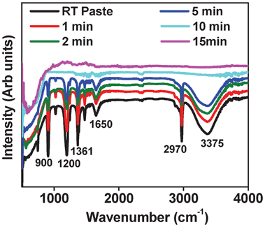 | ||
| Fig. 1 FTIR data of the as prepared paint taken at different time intervals at room temperature. | ||
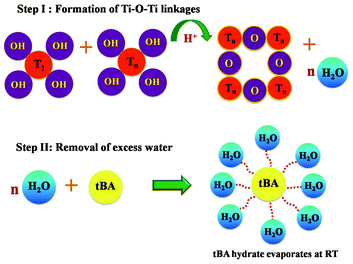 | ||
| Scheme 1 Mechanism for the formation of titania photoanode at room temperature. | ||
Fig. 2A shows the I–V data for three different cases (tBA: TiO2 ratio changing from 2 to 6) with all cells processed fully at room temperature. Table 1 gives the solar cell parameters. The electron micrographs shown in SI III† reveal changes in film morphology and microstructure with changing tBA![[thin space (1/6-em)]](https://www.rsc.org/images/entities/char_2009.gif) :TiO2 ratio (a ratio of tBA:TiO2 of 8 shows a very rough film with large microcracks hence solar parameters are poor and not shown). The data for optimization purposes were recorded only with a single point edge contact. The intermediate ratio of ∼4 yielded the highest efficiency at 3.6%. For a ratio of 6 the efficiency is close to the best case i.e. 3.3% while for a ratio of 2 the efficiency is low at 2.5%. Although the dye loading for tBA:TiO2 ratio of 2 is ∼10% higher than that for ratio 4, the cause of the low efficiency is the high degree of agglomeration in the TiO2 network which affects the interconnectivity between the TiO2 particulate system which leads to a higher degree of recombination. The interconnectivity is reflected by the transport resistance value across the active layer (as is mentioned in Fig. 4). Agglomeration tends to make mesoscale morphological features with nanoparticles attached to each other. The connectivity within the nanoparticles in a mesoscale object is good enough, but between such objects it is poorer, giving an overall higher transport resistance.
:TiO2 ratio (a ratio of tBA:TiO2 of 8 shows a very rough film with large microcracks hence solar parameters are poor and not shown). The data for optimization purposes were recorded only with a single point edge contact. The intermediate ratio of ∼4 yielded the highest efficiency at 3.6%. For a ratio of 6 the efficiency is close to the best case i.e. 3.3% while for a ratio of 2 the efficiency is low at 2.5%. Although the dye loading for tBA:TiO2 ratio of 2 is ∼10% higher than that for ratio 4, the cause of the low efficiency is the high degree of agglomeration in the TiO2 network which affects the interconnectivity between the TiO2 particulate system which leads to a higher degree of recombination. The interconnectivity is reflected by the transport resistance value across the active layer (as is mentioned in Fig. 4). Agglomeration tends to make mesoscale morphological features with nanoparticles attached to each other. The connectivity within the nanoparticles in a mesoscale object is good enough, but between such objects it is poorer, giving an overall higher transport resistance.
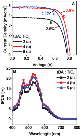 | ||
| Fig. 2 (A) I–V data and (B) IPCE data for tBA:TiO2 ratio of (a) 2 (b) 4 and (c) 6. | ||
| tBA:TiO2 | V oc (V) | J sc (mA cm−2) | FF (%) | η (%) |
|---|---|---|---|---|
| 2 | 0.77 | 3.82 | 68.74 | 2.5 |
| 4 | 0.81 | 4.82 | 73.76 | 3.6 |
| 6 | 0.78 | 4.88 | 70.1 | 3.3 |
An optimum tBA:TiO2 ratio of 4 clearly shows best efficiency due to improved necking between the particles. This in turn improves the fill factor (FF) and the open circuit voltage (Voc). For the tBA:TiO2 ratio of 6 the current is high but Voc and FF decrease due to the scattering of incoming light by larger TiO2 clusters.
Fig. 2B shows the incident photon to current conversion efficiency (IPCE) data for different cases. It follows the same trend as seen for the I–V data where the current density is highest for the ratio value of 4.
In addition to the ratio of solvent precursors, another important parameter that is required to be optimized for the best performance of the titania electrode for DSSC is film thickness. The effective optical absorption length, internal light scattering, series resistance etc. all depend on the thickness and morphology in a fairly complex way. This is all the more important for room temperature processing because the electronic grain connectivity, which is a critical parameter governing the optoelectronic performance has no thermal assistance in this case. Indeed the solvent evaporation under ambient temperature and pressure through an evolving grain constitution defines the final nano (micro) structure; its vertical (grain compaction and connectivity gradient) and lateral (stress, microcracking) uniformity. The lateral non-uniformity can result from drying shrinkage and the vertical one due to fluid density gradient. For very thin initial layers the effects of substrate-film interaction are important. Because of these factors we performed a detailed study of film thickness dependence and the relevant data are presented below. The I–V data for films of different thicknesses for our best efficiency case i.e. tBA:TiO2 ratio 4 are shown in Fig. 3. It can be seen from Table 2 that the 12 μm thick film gives the best result with better FF and Voc. It may be noted that the current density begins to drop for much thicker films.
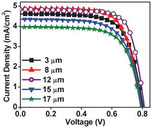 | ||
| Fig. 3 Thickness dependent I–V data with tBA:TiO2 ratio 4. | ||
| Name | Voc (V) | Jsc (mA cm−2) | FF (%) | η (%) |
|---|---|---|---|---|
| 3 μm | 0.80 | 4.62 | 68.7 | 2.5 |
| 8 μm | 0.79 | 4.80 | 70.1 | 2.7 |
| 12 μm | 0.81 | 4.82 | 73.8 | 3.6 |
| 15 μm | 0.79 | 4.30 | 67.3 | 2.3 |
| 17 μm | 0.78 | 3.96 | 69.3 | 2.2 |
The results of frequency dependent impedance studies for films of different thicknesses for our best efficiency case i.e. tBA: TiO2 ratio 4 are shown in Fig. 4B,C. The range chosen for the measurement was from 10−2 Hz to 106 Hz with an ac-amplitude of 10 mV. The general transmission line circuit is used to fit the plots shown in Fig. 4A.45 The impedance spectrum of DSSC mainly consists of three semicircles attributed to the interfaces between Pt/Electrolyte (Z1), TiO2|Dye/electrolyte (Z2) and diffusion of I3− (Z3) in the electrolyte, respectively.46Table 3 gives the parameters obtained from the impedance data. The results of current perpendicular to plane (CPP) DC electrical resistance measurements are summarized in Fig. 4D. The % transmittance data for various cases of interest are shown in ESI SI-IV†. The resistance of the photoelectrode as a whole is the sum of electron transport and recombination resistance obtained from the impedance data. Rt value of interest in this case is the electron transport resistance within the TiO2 network. It appears as linear in the impedance plot at an angle of ∼45.45 From the results the value of Rt is the lower for the film with a thickness ∼12 microns.
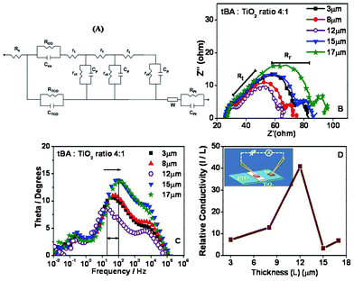 | ||
| Fig. 4 (A) Equivalent circuit, (B) Nyquist plot, (C) Bode plot and (D) Relative conductivity measurement with respect to film thickness for tBA:TiO2 ratio 4. | ||
:TiO2 ratio 4
| Thickness (μm) | 3 | 8 | 12 | 15 | 17 |
|---|---|---|---|---|---|
| R t (Ω) | 10.8 | 8.49 | 7.2 | 11.4 | 13.8 |
Also the keff value, which is the rate of recombination of electrons, can be calculated from the peak frequency of the central arc.47 The inverse of keff gives the lifetime (τ) of electrons throughout the working electrode and has a maximum value for the 12 μm film, compared to other films.
The direct current resistance of the photoanode can be obtained from current perpendicular to plane (CPP) conductivity data shown in Fig. 4D. Note that the current is divided by thickness to get a measure of conductivity. It is seen that CPP, conductivity is highest (and therefore resistance is lowest) for the 12 μm film. This signifies that the process of overall grain compaction and connectivity as controlled by the fluid drying process is optimal for this thickness value. Indeed, it may be further noted from the data shown in ESI SI-IV† that even from an optical standpoint the 12 μm film is poised for better performance. Thinner films do not absorb the full incident light and the absorption does not improve further by increasing thickness above 12 μm.
We explored the effect of annealing on the solar cell I–V characteristics. It is clear from the data shown in Fig. 5 that annealing at 150 °C, which is also an acceptable temperature for some polymeric substrates, leads to a moderate enhancement in current density, while annealing at 450 °C leads to a significant enhancement, as expected, due to better sintering of grains and hence improvements in the solar cell quality factors.
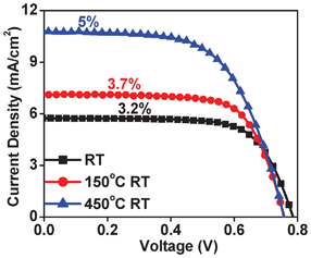 | ||
| Fig. 5 I–V data of cells made from solar paint at room temperature compared with those made from solar paint and annealed at 150 °C and 450 °C. | ||
The best paste with tBA:TiO2 ratio ∼4 was tested on a flexible substrate (ITO-PET). In this case we used a third layer of TiO2 spheres for light harvesting purposes.
Fig. 6A shows a typical I–V curve for the same paste, which shows an efficiency of 2.4% with Jsc = 5 mA cm−2, Voc of 0.8.V and FF of 61%. The inset shows the actual image of the dye-loaded flexible photoanode. The use of a simple and common hand-based technique for paste application, namely a paint brush, was investigated. Fig. 6B shows the I–V curve obtained using such a brush-painted photoanode, while the inset depicts the actual process of painting. A fairly high efficiency of 3% is realized, opening the way to easily paint DSSC directly on to FTO-coated smart window panes.
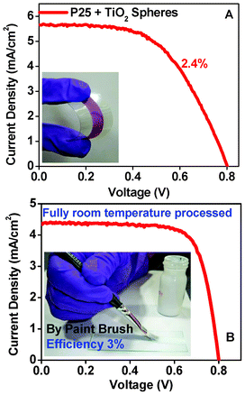 | ||
| Fig. 6 (A) I–V data and inset of actual images of flexible DSSC using solar paint (B) I–V data and inset of brush painted DSSC using solar paint. | ||
It may be noted that the efficiency values discussed earlier were obtained with a single point edge contact. To reduce the internal series resistance contribution (Rs) attributable to the transport resistance of the bottom and top contacts we examined U-type vapor deposited aluminum metal pads, shown in Fig. 7. This is equivalent to using conducting fingers in large area solar cell geometries. Although Voc decreased slightly, the current density increased substantially as is seen in Table 4. A conversion efficiency value of 5% was achieved. This result, although promising, needs to be consolidated by further work and detailed measurements.
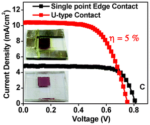 | ||
| Fig. 7
I–V data for plot for films with local and U-type Al contacts with tBA:TiO2 ratio 4 and thickness ∼12 microns. | ||
| Name | V oc (V) | J sc (mA cm−2) | FF (%) | η (%) |
|---|---|---|---|---|
| Single point edge contact | 0.81 | 4.8 | 73.7 | 3.6 |
| U type contact | 0.75 | 10.3 | 63.7 | 5.0 |
We also attempted fabrication of larger area (strip type, 5 mm × 56 mm) room temperature solar cell using this optimized solar paint. We could easily achieve a conversion efficiency of 3.1%. The film configuration and the I–V data are shown in ESI SI-V†.
Conclusions
In conclusion, we present a protocol for making room temperature curable titania-nanoparticle-based paint for easy application on hard as well as flexible substrates using a simple paint brush or other facile application methods (e.g. doctors blading, screen printing) to obtain fairly high conversion efficiency values. A conversion efficiency of 5% is obtained on FTO/glass substrates without any heat treatment or even an added light harvesting layer. Further optimization including use of a light harvesting layer will push this efficiency higher. We have achieved an efficiency of 2.4% on semi-transparent flexible ITO/PET substrate amenable to roll-to-roll processing. We believe that the room temperature curable solar paint developed and demonstrated in this work can be expanded further by incorporating other functional molecules such as dyes,48 quantum dots49 and electrolytes as well as carbon forms such as CNT50–52 and graphene to create novel photo-electrodes for sensitized solar cells, hybrid cells and other energy applications.Acknowledgements
The authors acknowledge funding from MNRE and CSIR (Govt. of India) under the TAPSUN program.References
- B. O'Regan and M. Gràtzel, Nature, 1991, 353, 737–740 CrossRef CAS.
- S. Muduli, O. Game, V. Dhas, A. Yengantiwar and S. B. Ogale, Energy Environ. Sci., 2011, 4, 2835–2839 CAS.
- D. Chen, F. Huang, Y.-B. Cheng and R. A. Caruso, Adv. Mater., 2009, 21, 2206–2210 CrossRef CAS.
- D. Kim, A. Ghicov, S. P. Albu and P. Schmuki, J. Am. Chem. Soc., 2008, 130, 16454–16455 CrossRef CAS.
- E. Ghadiri, N. Taghavinia, S. M. Zakeeruddin, M. Gràtzel and J.-E. Moser, Nano Lett., 2010, 10, 1632–1638 CrossRef CAS.
- F. Gao, Y. Wang, D. Shi, J. Zhang, M. Wang, X. Jing, R. Humphry-Baker, P. Wang, S. M. Zakeeruddin and M. Gràtzel, J. Am. Chem. Soc., 2008, 130, 10720–10728 CrossRef CAS.
- S. Ito, S. M. Zakeeruddin, R. Humphry-Baker, P. Liska, R. Charvet, P. Comte, M. K. Nazeeruddin, P. Péchy, M. Takata, H. Miura, S. Uchida and M. Grätzel, Adv. Mater., 2006, 18, 1202–1205 CrossRef CAS.
- R. Argazzi, N.-Y.-M. Iha, H. Zabri, F. Odobel and C. A. Bignozzi, Coord. Chem. Rev., 2004, 248, 1299–1316 CrossRef CAS.
- R. Y. Ogura, S. Nakane, M. Morooka, M. Orihashi, Y. Suzuki and K. Noda, Appl. Phys. Lett., 2009, 94, 073308 CrossRef.
- A. Allegrucci, N. A. Lewcenko, A. J. Mozer, L. Dennany, P. Wagner, D. L. Officer, K. Sunahara, S. Mori and L. Spiccia, Energy Environ. Sci., 2009, 2, 1069–1073 CAS.
- D. Kuang, P. Walter, F. Nüesch, S. Kim, J. Ko, P. Comte, S. M. Zakeeruddin, M. K. Nazeeruddin and M. Grätzel, Langmuir, 2007, 23, 10906–10909 CrossRef CAS.
- Y. Chen, Z. Zeng, C. Li, W. Wang, X. Wang and B. Zhang, New J. Chem., 2005, 29, 773–776 RSC.
- M. Wu, X. Lin, T. Wang, J. Qiu and T. Ma, Energy Environ. Sci., 2011 Search PubMed.
- A. Yella, H.-W. Lee, H. N. Tsao, C. Yi, A. K. Chandiran, M. K. Nazeeruddin, E. D. Wei-Guang, C.-Y. Yeh, S. M. Zakeeruddin and M. Grätzel, Science, 2011, 3344 Search PubMed.
- M. D. McGehee, Science, 2011, 334, 607–608 CrossRef CAS.
- T. Miyasaka, J. Phys. Chem. Lett., 2011, 2, 262–269 CrossRef CAS.
- N.-G. Park, K. M. Kim, M. G. Kang, K. S. Ryu, S. H. Chang and Y. J. Shin, Adv. Mater., 2005, 17, 2349–2353 CrossRef CAS.
- K.-M. Lee, S.-J. Wu, C.-Y. Chen, C.-G. Wu, M. Ikegami, K. Miyoshi, T. Miyasaka and K.-C. Ho, J. Mater. Chem., 2009, 19, 5009–5015 RSC.
- Y. Kijitori, M. Ikegami and T. Miyasaka, Chem. Lett., 2007, 36, 1 CrossRef.
- D. Zhang, T. Yoshida and H. Minoura, Adv. Mater., 2003, 15(10), 814–817 CrossRef CAS.
- Y. Li, W. Lee, D.-K. Lee, K. Kim, N.-G. Park and M. J. Ko, Appl. Phys. Lett., 2011, 98, 103301 CrossRef.
- L.-Y. Lin, C.-P. Lee, K.-W. Tsai, M.-H. Yeh, C.-Y. Chen, R. Vittal, C.-G. Wu and K.-C. Ho, Prog. Photovolt: Res. Appl, 2011 Search PubMed.
- X. Fan, Z. Chu, F. Wang, C. Zhang, L. Chen, Y. Tang and D. Zou, Adv. Mater., 2008, 20, 592–595 CrossRef CAS.
- P. Zhang, C. Wu, Y. Han, T. Jin, B. Chi, J. Pu and L. Jian, J. Am. Ceram. Soc., 2011, 1–6 Search PubMed.
- Y. Jiang, X. W Sun, K. W. Tan, G. Q. Lo, A. K. K. Kyaw and D. L. Kwong, Appl. Phys. Lett., 2008, 92, 143101 CrossRef.
- C.-H. Lee, W.-H. Chiu, K.-M. Lee, W.-F. Hsieh and J.-M. Wu, J. Mater. Chem., 2011, 21, 5114–5119 RSC.
- T. Miyasaka, M. Ikegami and Y. Kijitori, J. Electrochem. Soc., 2007, 154(5), A455–A461 CrossRef CAS.
- S. I. Cha, B. K. Koo, K. H. Hwang, S. H. Seo and D. Y. Lee, J. Mater. Chem., 2011, 21, 6300–6304 RSC.
- Q. Zeng, Y. Yu, L. Wu, B. Qi and J. Zhi, Phys. Status Solidi A, 2010, 207(9), 2201–2206 CrossRef CAS.
- Z. Wang, H. Wang, B. Liu, W. Qiu, J. Zhang, S. Ran, H. Huang, J. Xu, H. Han, D. Chen and G. Shen, ACS Nano, 2011, 5, 8412–8419 CrossRef CAS.
- S. Uchida, M. Tomiha, H. Takizawa and M. Kawaraya, J. Photochem. Photobiol., A, 2004, 164, 93–96 CrossRef CAS.
- Z. Tebby, T. Uddin, Y. Nicolas, C. Olivier, T. Toupance, C. Labrugere and L. Hirsch, ACS Appl. Mater. Interfaces, 2011, 3, 1485–1491 CAS.
- Z. Tebby, O. Babot, D. Michau, L. Hirsch, L. Carlos and T. Toupance, J. Photochem. Photobiol., A, 2009, 205, 70–76 CrossRef CAS.
- L. Grinis, S. Dor, A. Ofir and A. Zaban, J. Photochem. Photobiol., A, 2008, 198, 52–59 CrossRef CAS.
- T. Yamaguchi, N. Tobe, D. Matsumoto and H. Arakawa, Chem. Commun., 2007, 4767–4769 RSC.
- X. Yin, Z. Xue, L. Wang, Y. Cheng and B. Liu, ACS Appl. Mater. Interfaces, 2012, 4, 1709–1715 CAS.
- H. Lindstrom, A. Holmberg, E. Magnusson, S.-E. Lindquist, L. Malmqvist and A. Hagfeldt, Nano Lett., 2001, 1, 2 CrossRef.
- L. Grinis, S. Kotlyar, S. Ruhle, J. Grinblat and A. Zaban, Adv. Funct. Mater., 2010, 20, 282–288 CrossRef CAS.
- X. Liu, Y. Luo, H. Li, Y. Fan, Z. Yu, Y. Lin, L. Chen and Q. Meng, Chem. Commun., 2007, 2847–2849 RSC.
- A. K. K. Kyaw, X. W. Sun, J. L. Zhao, J. X. D. Wang, W. Zhao, X. F. Wei, X. W. Liu, H. V. Demir and T. Wu, J. Phys. D: Appl. Phys., 2011, 44, 045102 CrossRef.
- M. P. Genovese, I. V. Lightcap and P. V. Kamat, ACS Nano, 2012, 6, 865–872 CrossRef CAS.
- X. Chen and S. S. Mao, Chem. Rev., 2007, 107, 2891–2959 CrossRef CAS.
- K. Iwasak and T. Fujiyama, J. Phys. Chem., 1977, 81, 1908–1912 CrossRef.
- J. Korppi-Tommola, Spcctrochim. Acta, 1976, 34A, 1077–1085 Search PubMed.
- J. Halme, P. Vahermaa, K. Miettunen and P. Lund, Adv. Mater., 2010, 22, E210–E234 CrossRef CAS.
- M. Adachi, M. Sakamoto, J. Jiu, Y. Ogata and S. Isoda, J. Phys. Chem. B, 2006, 110, 13872–13880 CrossRef CAS.
- K.-M. Lee, C.-W. Hu, H.-W. Chen and K.-C. Ho, Sol. Energy Mater. Sol. Cells, 2008, 92, 1628–1633 CrossRef CAS.
- S. A. Agarkar, R. R. Kulkarni, V. V. Dhas, A. A. Chinchansure, P. Hazra, S. Joshi and S. B. Ogale, ACS Appl. Mater. Interfaces, 2011, 3, 2440–2444 CAS.
- W. Lee, S. K. Min, V. Dhas, S. B. Ogale and S.-H. Han, Electrochem. Commun., 2009, 11, 103–106 CrossRef CAS.
- S. Muduli, W. Lee, V. Dhas, S. Mujawar, M. Dubey, K. Vijayamohanan, S.-H. Han and S. B. Ogale, ACS Appl. Mater. Interfaces, 2009, 1, 2030–2035 CAS.
- A. K. K. Kyaw, H. Tantan, T. Wu, L. Ke, C. Peh, Z. H. Huang, X. T. Zeng, H. V. Demir, Q. Zhang and X. W. Sun, Appl. Phys. Lett., 2011, 99, 021107 CrossRef.
- H. Zhu, H. Zeng, V. Subramanian, C. Masarapu, K.-H. Hung and B. Wei, Nanotechnology, 2008, 19, 465204 CrossRef.
Footnote |
| † Electronic Supplementary Information (ESI) available. See DOI: 10.1039/c2ra22182a |
| This journal is © The Royal Society of Chemistry 2012 |