A simple and facile approach for synthesis of a free-standing TiO2 nanotube layer and its photovoltaic application†
Juanru
Huang
*ab,
Xin
Tan
ab,
Tao
Yu
*b,
Lin
Zhao
ab and
Song
Xue
c
aSchool of Environmental Science and Engineering, Tianjin University, Tianjin, 300072, China
bSchool of Chemical Engineering and Technology, Tianjin University, Tianjin, 300072, China
cDepartment of Applied Chemistry, Tianjin University of Technology, Tianjin, 300384, China. E-mail: hjr2002160@yahoo.com.cn; yutao@tju.edu.cn; Fax: 86-22-27891291
First published on 12th October 2012
Abstract
A vertically oriented, free-standing TiO2 nanotube (FS-TNT) layer was facilely fabricated via anodization and heat treatment, and the detaching mechanism of the FS-TNT layer is presented and authenticated. In addition, the closed-bottom-up FS-TNT layer after 2 h anodization facing the P25 film shows a significant improvement in the cell performance (η = 7.62%).
One-dimensional (1D) TNT arrays with well ordered arrangements and large specific areas, made from electrochemically anodized Ti substrates, attract extensive attention owing to their chemical stability, environmental friendliness, superior electron transport and small rate of charge recombination relative to conventional TiO2 nanoparticles. Although their fabricating factors, such as work voltage1,2 and current,1 electrolyte composition,3 reaction time2 and temperature4etc., have adequately been investigated, and related applied research in photocatalysis,2,5 water splitting,6 DSSCs,7 sensors and transducers,3 nanostructure templates and drug release platforms,8 have been carried out and revealed exciting performances, the FS-TNT array layer may have more interesting applications and better properties9,10 than the TNT array layers on opaque Ti substrates. Among them, a traditional 1D-TNT layer grown on a Ti substrate as the photoanode of a DSSC generally requires back-side illumination,11–13 and the TiO2 barrier layer attaching onto the substrate usually aggravates the photo-generated charge recombinations11,12 and/or obstructs molecular diffusion.14–16 In contrast, the FS-TNT array layers, which have already removed the Ti substrate, show a fascinating performance, including an optimized microstructure, direct electron transfer, superior light-conversion efficiency in front-illuminated DSSCs and they can be integrated or attached onto any foreign substrates.12,17,18
So far, various techniques used to fabricate the FS-TNT layer with different thicknesses have been reported. High-aspect ratio FS-TNT layers with thicknesses of 134 μm,13 720 μm,19 and 1000 μm16 are assembled by completely anodizing Ti substrates, and then utilized to investigate their diffusion and biofiltration.16,20 Mechanical delamination, containing solvent evaporation,15,21 ultrasonic vibration,14,21 and direct detachment,22 is implemented to separate the TNT layer from the Ti substrate. Some preparative conditions, such as the work voltage,23–25 the electrolyte temperature26 and the composition,27 are effectively regulated to strip off the TNT layer. Chemical dissolution, for instance, the mixture of Br2 and dry methanol,9 HF,28 H2O2,11,12 HCl29 and HgCl2,30 is selectively employed to attain the FS-TNT layer. Most of the above approaches either result in cracked, curling and even fractional FS-TNT layers, or require delicate and complicated procedures, or corrosive and hazardous reagents. Recently, the front-illuminated DSSCs with the closed-bottom-up FS-TNT layers (the closed bottom of FS-TNT layers is up) facing TiO2 nanoparticles (CBU FS-NPs, configuration) exhibit better photovoltaic performance than the front-illuminated cells with the open-top-up (the open top of FS-TNT layers is up) FS-NPs (OTU FS-NPs, configuration)28,31 and the corresponding back-illuminated DSSCs with the TNT layers on opaque Ti substrates.11 The thickness of the TNT layer plays a crucial role in the performance of the front-illuminated and/or back-illuminated DSSCs.10,28,32
In this work, we introduce a simple and facile approach with a detailed procedure for the synthesis of the FS-TNT array layer, with an open and closed bottom via anodization and heat treatment. Due to the varying resistance to chemical corrosion, and the mechanical stability between the annealed top and amorphous bottom layers, the top layer was annealed at 250–650 °C and is lifted off from the bottom layer on the Ti substrate at 45 °C electrolyte. Based on the FE-SEM and XRD measurement, the detaching mechanism of the FS-TNT array layer is presented and further verified by XPS and EDX. Furthermore, the front-illuminated DSSC with the CBU configuration significantly improves the cell performance (η = 7.62%) over those of the counterpart with the P25 film (η = 4.78%).
The experimental section (experimental details are given in the ESI†) reveals that only in electrolyte at 45 °C can the annealed top layer be favourably detached from the amorphous bottom layer formed on the Ti substrate in the third anodization (see Fig. 2b). At a lower temperature (<45 °C) the top layer tightly connects with the amorphous bottom layer on the Ti substrate and/or at a higher temperature (>45 °C) the top layer fragments gradually and then floats in the electrolyte. These results show the F− ions at 45 °C electrolyte probably play a key role in this detaching process.
FE-SEM images of the FS2-TNT layer with an open bottom, a closed bottom and a closed bottom coated with an old TiO2 barrier layer (see Fig. 2b) are shown in Fig. 1. Specifically, the FS2-TNTs with completely and partially open bottoms (Fig. 1(a, b)) are facilely achieved when the TNT layers annealed at 250 °C and 300 °C were re-anodized in the third reaction, respectively. The images obtained from the annealing of FS2-TNTs with closed bottoms at 350 °C, 400 °C and 450 °C, are shown in Fig. 1(c–e). An increase in temperature to 500 °C, showed that the closed-bottom FS2-TNTs with partially old TiO2 barrier layers are revealed (Fig. 1f). This increase in temperature to 550 °C and 650 °C, shows that the FS2-TNTs bottoms are completely covered by a thin and thick old barrier layer (see Fig. 1(g–h)), respectively. Furthermore, the tops of the FS2-TNTs have seriously collapsed (see the insets of Fig. 1g and Fig. 1c, as well as the insets of Fig. 1(a, d)), which also demonstrates the bottom morphology of the FS-TNT layers, and shows the pseudo regular-hexagon patterns on the Ti substrates.33,34
 | ||
| Fig. 1 FE-SEM images of the FS2-TNT bottoms annealed at (a) 250 (b) 300 (c) 350 (d) 400 (e) 450 (f) 500 (g) 550 and (h) 650 °C. The insets of (a, d) are the magnified images, the inset of (g) is the top image. | ||
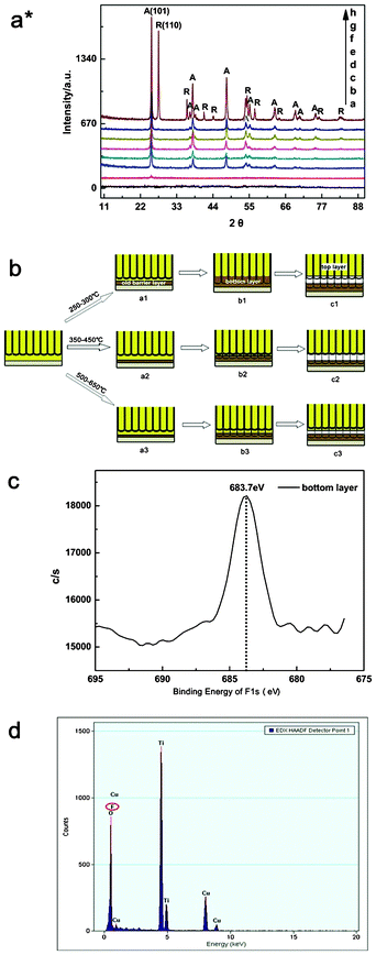 | ||
| Fig. 2 (a*) XRD spectra of the FS4-TNT layer annealed at (a) 250 (b) 300 (c) 350 (d) 400 (e) 450 (f) 500 (g) 550 and (h) 650 °C. “A” = anatase, “R” = rutile. (b) The schematic diagram of detaching FS-TNT layers with annealing temperatures between 250–300 °C, 350–450 °C and 500–650 °C, (c) XPS and (d) EDX spectra of the FS3-TNT layers annealed at 350 °C and 450 °C, respectively. | ||
XRD spectra of the FS4-TNT layers annealed at temperatures of 250–650 °C are shown by the curves (a–h) in Fig. 2a*, and the letters A and R note the anatase and rutile phases, respectively. Compared to JCPDS (No. 21-1272 and 21-1276), the samples sintered at 250 °C and 300 °C are almost amorphous, except for a weak A (101) peak in curve (b). At annealing temperatures of 350 °C, 400 °C and 450 °C, the single A phase with various planes is shown by the curves (c–e), and continues to be seen at 500 °C and 550 °C. The weak R peaks are indicated by the curves (f, g) until 650 °C, when the intense R (110) peak is definitively marked by the curve (h). These results illustrate that the intense A peaks appear in the spectra of FS4-TNTs calcined at 450 °C, and the phase transition with the amorphism to A, and A to R occurs at 300 °C and 500 °C, respectively.
Based on the FE-SEM and XRD measurements, the detaching mechanism of the annealed FS-TNT layer is shown by the schematic diagram in Fig. 2b. (1) When the anodized Ti substrate, which is pre-annealed at 250–300 °C, is again anodized, the annealed top layer (the FS-TNTs with open bottoms) is detached from the bottom layer on the Ti substrate (see Fig. 2b (a1–c1)) during the reaction. In the reaction, the O2−/OH− ions in the electrolyte move to the interface of the old barrier layer–Ti substrate, and then react with the Ti substrate to form the new TiO2 barrier layer (Ti + 2H2O → TiO2 + 4H+ + 4e−) (Fig. 2b-a1). A two barrier layer with a predominantly amorphous structure possesses a weak difference in chemical resistance and mechanical stability in the 45 °C electrolyte.11,12,26,35 A new partial barrier layer with a certain thickness, therefore, begins to form on the TNTs when the old barrier layer has completely formed as shown in Fig. 2b-b1. The former TNTs from the new barrier layer are corroded preferentially by the F− ions (TiO2 + F− + H+ → (TiF6)2− + H2O) in the electrolyte (see Fig. 2b-c1), due to the feeble chemical resistance and the longer time spent in the electrolyte bath than the latter. Finally, the FS-TNTs with open bottoms (Fig. 1(a, b)) are achieved. (2) At annealing temperatures of 350 °C, 400 °C and 450 °C, the TNTs with an A phase decelerate the migration of the O2−/OH− ions to the old barrier layer/Ti substrate and the F− to the TNT/old barrier layer in the electrolyte. The rate of formation of the new barrier layer, however, is relatively faster than that of the TNTs from the old barrier layer. This brings about a new barrier layer with a certain thickness in the TNTs, along with the thinner old barrier layer which remains (Fig. 2b-b2). When the F− etched the residual old barrier layer completely, the TNTs formed first from the new barrier layer have just been corroded by F−, and thus the FS-TNTs with closed bottoms (Fig. 1(c–e)) are detached from the bottom layer (Fig. 2b-c2). (3) At the temperatures of 500 °C, 550 °C and 650 °C, the R phase appears, and at 650 °C the intense R (110) peak (see Fig. 2a*) shows that the top layer possesses a stronger corrosion resistance and mechanical stability to the F− ions in the electrolyte. When the TNTs from the new barrier layer were formed, the residual new barrier layer and thicker old barrier layer remained (Fig. 2b(a3,b3)). During the reaction, the annealed top layer with the varying-thickness old barrier layer (see Fig. 1(f–h)) is gradually separated from the third-anodized Ti substrate (Fig. 2b-c3).
Afterwards, XPS measured the chemical composition and binding energy of the top, the bottom of the FS3-TNT layer and the bottom layer with the Ti substrate (bottom layer in Fig. 2c) sintered at 350 °C. The binding energy peaks of C1s, O1s, Ti2p and N1s were all investigated in the samples, but only the F1s (683.7 eV) peak deviating from the standard peak (686.0 eV) was detected (Fig. 2c). This result shows that the F− in 45 °C electrolyte preferentially etched the amorphous bottom layer with the weakest resistance, and thus the residual F− remained in the bottom layer, even if the sample was annealed at 350 °C. This was also verified by EDX measurements (Fig. 2d). Still, other samples can also be manifested in the same way.
The FS-TNT layer with a controllable morphology and thickness can be fabricated in the light of this approach (experimental details are given in the ESI†). The thicknesses of the TNT layer with the Ti substrate and the FS2-TNT layer detaching from the bottom layer are 7.82 and 7.86 μm (see Fig. S(a, b), ESI†), respectively, which shows that the TNT layer before and after the detaching is of nearly equal thickness. The front-illuminated DSSC with a CBU configuration has been also fabricated (experimental details are given in the ESI†). Recent reports have proved that the thickness of the TNT layer and the interface between the FS-TNT layer and the TiO2 nanoparticle film plays a crucial role in DSSC efficiency.10,11,28,32 In particular, the DSSC based on the FS-TNT layer with a suitable thickness reveals the optimal performance of the front-illuminated cell.10,28,32 The front-illuminated DSSC with the CBU configuration displays a more superior performance than the corresponding back-illuminated DSSC with the TNT layer on an opaque Ti substrate.11 In this work, the interfacial contact between the TNT layers and the P25 particle film (see Fig. S(c, d), ESI†) indicates that the CBU configuration shows better contact properties than the OTU configuration, which is in accordance with the work in reference 28. The cell with the CBU configuration exhibits better interfacial contact between the TNTs and NPs, a higher external quantum efficiency, a greater charge transfer resistance from the FTO/TiO2 to the electrolyte and better dye loading compared to the cell with the OTU configuration.28
In view of the above, the CBU FS2-P25 configuration as the photoanode film is used to illustrate the photovoltaic application of the FS-TNT layer. Herein, the CBU configuration with a FTO substrate as the photoanode is fabricated for the front-illuminated DSSC, the J–V and IPCE characteristics of the representative samples are shown in Fig. 3. The DSSC with the CBU configuration exhibits higher Jsc, Voc, FF and η than the DSSC with a 9.5 μm P25 film (Fig. 3). The CBU configuration with the larger surface area enhances the incident-light capture and further improves the photoelectron injection from the CBU configuration to the FTO. The P25 paste fills the interfacial gaps between the TNT arrays, and the FTO greatly strengthens the connection at the interface,28,31 and then effectively improves the transfer and collection of photo-generated charges. In addition, the 1D TNT layer decreases the TiO2 grain boundary and reduces the amount of charge recombination in the CBU configuration, which results in an increase of Jsc and an improved η. In Fig. 3b, the two cells show an impressive response, with λ = 400 nm–650 nm, and the IPCE of the CBU cell reaches up to 0.70 at 550 nm compared to the P25 cell with IPCE of 0.38, which is attributed to the more N719 absorbed on the CBU configuration, in accordance with the data in Fig. 3. Therefore, incident light with higher harvesting efficiency is attained, and more photo-generated charges enter into the external circuit. From the above, the front-illuminated DSSC with the CBU configuration shows a significantly improved cell performance over that of the cell with the P25 film.
 | ||
| Fig. 3 J–V (a) and IPCE (b) curves of the front-illuminated DSSCs, based on the CBU FS2-P25 configuration and the P25 films. | ||
FS-TNT layers with an open bottom, a closed bottom and a closed bottom with an old barrier layer detached from the amorphous bottom were grown on an opaque Ti substrate via heat treatment at 250–650 °C and followed by subsequent re-anodization. Based on the characterizations, the detaching mechanism of the annealed FS-TNT layer is represented and further confirmed. Furthermore, the CBU configuration is used to fabricate the front-illuminated DSSC with significant improvements.
This work was supported by the National Basic Research Program of China (973 program, No.202CB720100) and the National Natural Science Foundation of China (No.20973124).
References
- L. L. Li, C. Y. Tsai, H. P. Wu, C. C. Chen and E. W. G. Diau, J. Mater. Chem., 2010, 20, 2753–2819 RSC.
- S. Sreekantan, K. A. Saharudin, Z. Lockman and T. W. Tzu, Nanotechnology, 2010, 21, 365603 CrossRef.
- Z. X. Su and W. Z. Zhou, J. Mater. Chem., 2011, 21, 8955–8970 RSC.
- Z. B. Xie and D. J. Blackwood, Electrochim. Acta, 2010, 56, 905–912 CrossRef CAS.
- S. I. In, M. G. Nielsen, P. C. K. Vesborg, Y. Hou, B. L. Abrams, T. R. Henriksen, O. Hansen and I. Chorkendorff, Chem. Commun., 2011, 47, 2613–2615 RSC.
- N. K. Allam, K. Shankar and C. A. Grimes, J. Mater. Chem., 2008, 18, 2341–2348 RSC.
- S. Agarwala and G. W. Ho, J. Solid State Chem., 2012, 189, 101–107 CrossRef CAS.
- Y. Y. Song, F. Schmidt-Stein, S. Bauer and P. Schmuki, J. Am. Chem. Soc., 2009, 131, 4230–4232 CrossRef CAS.
- S. P. Albu, A. Ghicov, J. M. Macak, R. Hahn and P. Schmuki, Nano Lett., 2007, 7, 1286–1289 CrossRef CAS.
- P. T. Hsiao, Y. J. Liou and H. S. Teng, J. Phys. Chem. C, 2011, 115, 15018–15024 CAS.
- Q. W. Chen and D. S. Xu, J. Phys. Chem. C, 2009, 113, 6310–6314 CAS.
- C. J. Lin, W. Y. Yu and S. H. Chien, J. Mater. Chem., 2010, 20, 1073–1077 RSC.
- M. Paulose, K. Shankar, S. Yoriya, H. E. Prakasam, O. K. Varghese, G. K. Mor, T. A. Latempa, A. Fitzgerald and C. A. Grimes, J. Phys. Chem. B, 2006, 110, 16179–16184 CrossRef CAS.
- Q. Q. Chen, D. S. Xu, Z. Y. Wu and Z. F. Liu, Nanotechnology, 2008, 19, 365708 CrossRef.
- X. Meng, T. Y. Lee, H. Chen, D. W. Shin, K. W. Kwon, S. J. Kwon and J. B. Yoo, J. Nanosci. Nanotechnol., 2010, 10, 4259–4265 CrossRef CAS.
- M. Paulose, H. E. Prakasam, O. K. Varghese, L. Peng, K. C. Popat, G. K. Mor, T. A. Desai and C. A. Grimes, J. Phys. Chem. C, 2007, 111, 14992–14997 CAS.
- K. V. Oomman, M. Paulose and C. A. Grimes, Nat. Nanotechnol., 2009, 4, 59–597 Search PubMed.
- G. K. Mor, K. Shankar, M. Paulose, O. K. Varghese and C. A. Grimes, Nano Lett., 2006, 6, 215–218 CrossRef CAS.
- H. E. Prakasam, K. Shankar, M. Paulose, O. K. Varghese and C. A. Grimes, J. Phys. Chem. C, 2007, 111, 7235–7241 CAS.
- M. Paulose, L. L. Peng, K. C. Popat, O. K. Varghese, T. A. Latempa, T. A. Bao, T. A. Desai and C. A. Grimes, J. Membr. Sci., 2008, 319, 199–205 CrossRef CAS.
- J. W. Ng, X. W. Zhang, T. Zhang, J. H. Pan, J. H. A. Du and D. D. Sun, J. Chem. Technol. Biotechnol., 2010, 85, 1061–1066 CrossRef CAS.
- S. Singh, M. Festin, W. R. T. Barden, L. Xi, J. T. Francis and P. Kruse, ACS Nano, 2008, 2, 2363–2373 CrossRef CAS.
- Y. Jo, I. Jung, I. Lee, J. Choi and Y. Tak, Electrochem. Commun., 2010, 12, 616–619 CrossRef CAS.
- K. Kant and D. Losic, Phys. Status Solidi RRL, 2009, 3, 139–141 CrossRef CAS.
- D. A. Wang and L. F. Liu, Chem. Mater., 2010, 22, 6656–6664 CrossRef CAS.
- J. Lin, J. F. Chen and X. F. Chen, Electrochem. Commun., 2010, 12, 1062–1065 CrossRef CAS.
- X. L. He, Y. Y. Cai, H. M. Zhang and C. H. Liang, J. Mater. Chem., 2011, 21, 475–480 RSC.
- M. Dubey, M. Shrestha, Y. Zhong, D. Galipeau and H. He, Nanotechnology, 2011, 22, 285201 CrossRef.
- J. H. Park, T. W. Lee and M. G. Kang, Chem. Commun., 2008, 2867–2869 RSC.
- D. A. Wang, B. Yu, C. W. Wang, F. Zhou and W. M. Liu, Adv. Mater., 2009, 21, 1964–1967 CrossRef CAS.
- L. L. Li, Y. J. Chen, H. P. Wu, N. S. Wang and E. W. G. Diau, Energy Environ. Sci., 2011, 4, 3420–3425 CAS.
- B. X. Lei, J. Y. Liao, R. Zhang, J. Wang, C. Y. Su and D. B. Kuang, J. Phys. Chem. C, 2010, 114, 15228–15233 CAS.
- S. Q. Li, G. M. Zhang, D. Z. Guo, L. G. Yu and W. Zhang, J. Phys. Chem. C, 2009, 113, 12759–12765 CAS.
- Y. Shin and S. Lee, Nano Lett., 2008, 8, 3171–3173 CrossRef CAS.
- J. M. Macak, S. Aldabergerova, A. Ghicov and P. Schmuki, Phys. Status Solidi A, 2006, 203, R67–R69 CrossRef CAS.
Footnote |
| † Electronic supplementary information (ESI) available. See DOI: 10.1039/c2ra22059h |
| This journal is © The Royal Society of Chemistry 2012 |