One-step solution-based synthesis and characterization of kuramite Cu3SnS4 nanocrystals†
Xianzhong
Lin
*,
Alexander
Steigert
,
Martha Ch.
Lux-Steiner
and
Ahmed
Ennaoui
*
Helmholtz-Zentrum Berlin für Materialien und Energie GmbH, Hahn-Meitner-Platz 1, Berlin, 14109, Germany. E-mail: lin.xianzhong@helmholtz-berlin.de; ennaoui@helmholtz-berlin.de; Fax: + 49 30 806243199; Fax: + 49 30 806243199; Tel: + 49 30 8062 42579 Tel: + 49 30 8062 43038
First published on 31st August 2012
Abstract
Kuramite Cu3SnS4 nanocrystals with tetragonal structure have been synthesized by a simple one-step solution-based process and characterized in detail by X-ray diffraction, transmission electron microscopy, energy dispersive X-ray spectroscopy and X-ray photoelectron spectroscopy. The nanocrystals show an optical band gap of 1.43 eV as estimated from the UV-vis-NIR spectrum.
Copper-based multinary chalcogenide semiconductor materials such as CuInS(Se)2, Cu(In,Ga)S(Se)2 and Cu2ZnSnS(Se)4 (CZTSSe) have attracted increasing attention due to their potential application in photovoltaic, thermoelectric and photocatalytic devices.1–9 Thin film solar cells based on Cu(In,Ga)Se2 have achieved efficiencies slightly over 20%.2 However, due to the scarcity of the indium constituent, these materials cannot meet the long term goal of solar energy development. To solve this issue, it is necessary to develop alternative light absorbing materials which are composed of relatively earth abundant elements. In recent years, kesterite CZTS has emerged as a promising candidate for thin film solar cells because of its direct optical band gap of 1.5 eV, high absorption coefficient (104 cm−1) in the visible region and relatively available constituents. Although CZTSSe-based solar cells have reached efficiencies as high as 10.1%,3,4 the structural complex and relatively small existence region in the phase diagram make these material systems a great challenge for high performance solar cells.10 Similar to CuInS2, kuramite Cu3SnS4 (CTS) is a p-type semiconductor material,11–13 however it contains much more earth-abundant constituents. CTS, belonging to the stannite group (I
![[4 with combining macron]](https://www.rsc.org/images/entities/char_0034_0304.gif) 2m), has attracted great attention due to its potential application in thin film solar cells.11 The optical band gap of 1.2–1.6 eV11–16 and the absorption coefficient of around 104 cm−111–14 make CTS a promising candidate for potential applications in photovoltaics. To the best of our knowledge, kuramite CTS nanoparticles,13,17 nanorods18 and nanoshell tubes19 have been prepared mainly by the solvothermal reaction route. However, there are a few reports on the synthesis of kuramite CTS nanocrystals using colloidal routes. Recently, Yi et al.16 reported a colloidal synthesis of orthorhombic CTS nano-cuboids and nanosheets using monoclinic Cu31S16 nanocrystals as seeds. However, the procedure of this preparation is complicated and formation of CTS nanocrystals requires a long reaction time of over four hours. In this work, we report on a simple synthesis of kuramite CTS nanocrystals following a one pot technique using oleylamine as a solvent and capping agent.
2m), has attracted great attention due to its potential application in thin film solar cells.11 The optical band gap of 1.2–1.6 eV11–16 and the absorption coefficient of around 104 cm−111–14 make CTS a promising candidate for potential applications in photovoltaics. To the best of our knowledge, kuramite CTS nanoparticles,13,17 nanorods18 and nanoshell tubes19 have been prepared mainly by the solvothermal reaction route. However, there are a few reports on the synthesis of kuramite CTS nanocrystals using colloidal routes. Recently, Yi et al.16 reported a colloidal synthesis of orthorhombic CTS nano-cuboids and nanosheets using monoclinic Cu31S16 nanocrystals as seeds. However, the procedure of this preparation is complicated and formation of CTS nanocrystals requires a long reaction time of over four hours. In this work, we report on a simple synthesis of kuramite CTS nanocrystals following a one pot technique using oleylamine as a solvent and capping agent.
Powder X-ray diffraction (PXRD), a powerful tool for characterization of crystal structures, was used to determine the crystal structure of the obtained nanocrystals, shown in Fig. 1. When comparing the experimental result with the standard patterns of kuramite CTS (JCPDS card 33-0501), we found that all the diffraction peaks match quite well with kuramite CTS, indicating that the as-synthesized nanocrystals are CTS with a tetragonal structure. Note that the most pronounced diffraction peak of the experimental diffraction pattern is (112), which is different from that of the standard JCPDS card 33-0501 where the most intensive peak is (220). This difference may suggests that the as-synthesized CTS nanocrystals exhibit preferential orientation along (112). The average crystalline size is calculated to be 14 nm by the Scherer equation D = Kλ/(βcosθ), where K is a constant (0.9), λ is the wavelength of the X-ray (1.5406 Å), β is the full width half maximum, and θ is the Bragg angle of the (112) Bragg peak.
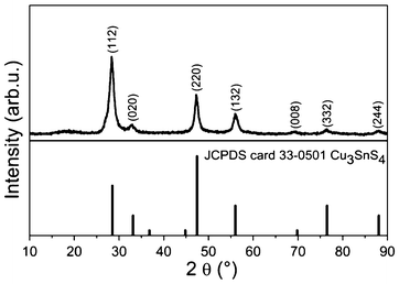 | ||
| Fig. 1 PXRD patterns of as-synthesized CTS nanocrystals. For reference, the standard PXRD patterns of kuramite Cu3SnS4 is shown below. | ||
The morphology of the as-synthesized kuramite CTS nanocrystals was characterized by TEM. Fig. 2(a) is a low magnification image of the CTS nanocrystals which shows that the nanocrystals are slightly irregular shape. The corresponding size distribution histogram (Fig. 2(b)) reveals that the average size of the nanocrystals is 16.1 nm with a standard deviation of 2.9 nm. This value is in agreement with that estimated from PXRD by the Scherer equation. Fig. 2(c) shows the high resolution image of a single CTS nanocrystal, which displays clear lattice fringes throughout the whole particle indicating the high crystalline quality of the nanocrystals. The spacing of the lattice fringes was measured to be 0.313 nm, which matches the (112) plane of CTS. This result implies that the preferred orientation of CTS naoncrystals is (112), which is in accordance with the PXRD result. Fig. 2(d) shows a representative EDX spectrum of the nanocrystal samples. All elements, Cu, Sn, and S, were detected in the nanocrystals. Moreover, the inset table reveals the average ratio of Cu![[thin space (1/6-em)]](https://www.rsc.org/images/entities/char_2009.gif) :Sn:S is 40.6:13.5:45.9 as determined by analysing five randomly selected areas. This value is close to the stoichiometry of Cu3SnS4 but slightly sulfur poor, providing further evidence that the obtained nanocrystals are kuramite CTS.
:Sn:S is 40.6:13.5:45.9 as determined by analysing five randomly selected areas. This value is close to the stoichiometry of Cu3SnS4 but slightly sulfur poor, providing further evidence that the obtained nanocrystals are kuramite CTS.
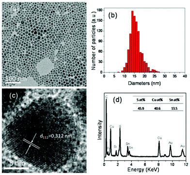 | ||
| Fig. 2 (a) Low resolution TEM image of as-synthesized CTS nanocrystals on a carbon film coated gold grids; (b) Corresponding histogram of particle size distribution; the average size of the nanocrystals is (16.1 ± 2.9) nm. (c) High resolution TEM image of a single CTS nanocrystal; (d) EDX spectrum of CTS nanocrystals. The inset shows the table of composition. | ||
For profound understanding of the oxidation states of the elements in CTS nanocrystals, XPS measurements were performed on the CTS sample deposited on molybdenum coated glass substrate by drop casting. A survey spectrum, Fig. 3(a), identified the presence of Cu, Sn, S, O and C, which is in good agreement with the EDX results. The deposition process has been carried out in air and the naoncrystals were capped by oleylamine, which explains the content of O and C. The Cu2p3/2 core-level (Fig. 3(b)) is located at 932.3 eV binding energy. This value is close to the reported values for compounds with Cu(I), such as in Cu2S, and confirmed the existence of the Cu(I) state in the CTS samples. A weak shoulder and broadening of the Cu2p3/2 peak is observed. However, it can not be identified if this stems from a Cu(II) oxidation state in CTS or is a second component due to surface contamination. A satellite peak at higher binding energies, such as is found for CuO, is not observed. Fig. 3(c) reveals the Sn3d5/2 peak centered at 486.5 eV, indicating the Sn(IV) state in the CTS samples.13,19 The S2p core-level spectrum (Fig. 3(d)) shows two peaks at 161.9 eV and 163.0 eV, which imply that S is in sulfide state.13,19 Note that a sulfate peak at around 169 eV was also observed during the measurement, which is not shown in the S2p spectrum. This suggests the oxidation of the samples due to exposure to air. Therefore, for an optimal XPS analysis, a further improvement of the deposition process is necessary to reduce the contamination.
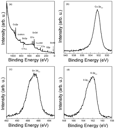 | ||
| Fig. 3 XPS spectra of CTS nanocrystals: (a) typical survey spectrum, (b) Cu 3/2p core level, (c) Sn3d core level, and (d) S2p core level. | ||
We have studied the growth of the CTS nanocrystals by taking aliquots at different reaction times from the reaction vessel and analyzing them with PXRD, TEM and EDX. Fig. S1† shows the PXRD patterns of samples taken out at different reaction times. It can be seen that all samples show similar PXRD patterns with all the peaks matching with kuramite CTS very well, indicating that we can get kuramite CTS nanocrystals after reaction time of 5 min. Table S1† shows the average value of EDX analysis on five randomly selected areas in each sample. As can be seen, the composition of the nanocrystals is nearly stable by keeping the ratio of Cu:Sn:S close to the stoichiometry of Cu3SnS4. The results of PXRD and EDX analysis confirmed that the CTS nanocrystals can be synthesized in a short reaction time of 5 min. Fig. S2† shows the TEM images and the corresponding size distribution histogram. As the reaction time increased from 5 min to 45 min, the average size of the nanocrystals increased from 10.7 ± 4.1 nm to 16.4 ± 3.5 nm due to the Ostwald ripening of the nanocrystals. Generally, in a classic steady-state Ostwald ripening large particles grow larger and larger with the sacrifice of the smaller particles, resulting in increasing particle size and a broadening size distribution. However, there is a transient stage of Ostwald ripening before starting the classic steady-state Ostwald ripening according to Peng et al.20 who studied the growth of MnO nanocrystals and observed the transient stage during the growth of the MnO nanocrystals. The feature of the transient stage is that the size of the nanocrystals increases slowly, as well as the decrease of the size distribution. In our reaction system, the slow growth of the nanocrystals can be explained by the experience of transient stage Ostwald ripening. It seems that a longer reaction time is needed in our CTS system in order to observe the classic steady-state Ostwald ripening.
To better understand the effect of reaction conditions on the final products, we performed several contrast experiments. For example, when the ratio of the precursors of Cu:Sn:S changed from 2:1:3 to 3:1:4, we found that nearly monodisperse nanocrystals with 13.4 ± 1.9 nm (Fig. S4†) can be obtained. However, PXRD (Fig. S4†) shows that Cu1.97S and Sn3S4 phases were also observed besides the CTS phase, indicating that precise control of the precursors ratio is important in order to acquire single phase CTS.
UV-vis absorption spectroscopy was used to evaluate the optical properties of the nanocrystals. Fig. 4 shows that the nanocrystals exhibit high absorption in the visible region. The optical band gap is 1.43 eV as estimated by extrapolating the linear part of the plot (αhυ)2, the square of the absorption coefficient (α) multiplied by the photon energy (hυ), versus hυ. This value is consistent with the literature values of 1.2–1.6 eV.12,13,15
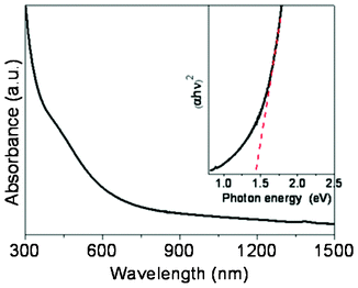 | ||
| Fig. 4 UV-vis-NIR absorption spectrum of CTS nanocrystals dispersed in toluene. Inset is the plot of (αhυ)2versus hυ (eV) for the nanocrystals. | ||
In conclusion, we proposed a facile one-step solution-based approach for the synthesis of kuramite CTS nanocrystals with tetragonal structure. The kuramite CTS nanocrystals can be obtained in a short reaction time of 5 min. EDX and XPS analysis confirmed the existence of all three elements in the nanocrystals. The estimated band gap of the CTS nanocrystals is 1.43 eV, which is optimal for solar energy conversion. Further application of this material in photovoltaics is in progress.
This work was carried out as part of a program supported by the BMBF (Grant 03SF0363B). The authors would like to thank Ulrike Bloeck for the TEM measurements. One of the authors (Xianzhong Lin) gratefully acknowledges the financial support from the Chinese Scholarship Council, HZB and Helmholtz Association.
References
- A. Chirilă, S. Buecheler, F. Pianezzi, P. Bloesch, C. Gretener, A. R. Uhl, C. Fella, L. Kranz, J. Perrenoud, S. Seyrling, R. Verma, S. Nishiwaki, Y. E. Romanyuk, G. Bilger and A. N. Tiwari, Nat. Mater., 2011, 10, 857 CrossRef
.
- P. Jackson, D. Hariskos, E. Lotter, S. Paetel, R. Wuerz, R. Menner, W. Wischmann and M. Powalla, Prog. Photovoltaics, 2011, 19, 894 CAS
- B. Shin, O. Gunawan, Y. Zhu, N. a. Bojarczuk, S. J. Chey and S. Guha, Prog. Photovoltaics, 2012, 20, 6 Search PubMed
- S. Bag, O. Gunawan, T. Gokmen, Y. Zhu, T. K. Todorov and D. B. Mitzi, Energy Environ. Sci., 2012, 5, 7060 CAS
- M.-L. Liu, F.-Q. Huang, L.-D. Chen and I.-W. Chen, Appl. Phys. Lett., 2009, 94, 202103 CrossRef
- H. Yang, L. A. Jauregui, G. Zhang, Y. P. Chen and Y. Wu, Nano Lett., 2012, 12, 540 CrossRef CAS
- A. Ennaoui, M. Lux-steiner, A. Weber, D. Abou-ras, I. Kötschau, H. Schock, R. Schurr, A. Hölzing, S. Jost, R. Hock, T. Voß, J. Schulze and A. Kirbs, Thin Solid Films, 2009, 517, 2511 CrossRef CAS
- X. Lin, J. Kavalakkatt, K. Kornhuber, D. Abou-Ras, S. Schorr, M. Ch. Lux-Steiner and A. Ennaoui, RSC Adv., 2012 10.1039/C2RA21293E
- L. Wang, W. Wang and S. Sun, J. Mater. Chem., 2012, 22, 655 Search PubMed
- S. Siebentritt and S. Schorr, Prog. Photovoltaics, 2012, 20, 512 CAS
- P. A Fernandes, P. M. P. Salomé and F. D. Cunha A, J. Phys. D: Appl. Phys., 2010, 43, 215403 CrossRef
- M. Bouaziz, J. Ouerfelli, M. Amlouk and S. Belgacem, Phys. Status Solidi A, 2007, 204, 3354 CrossRef CAS
- Z. Su, K. Sun, Z. Han, F. Liu, Y. Lai, J. Li and Y. Liu, J. Mater. Chem., 2012, 22, 16346 RSC
- M. Bouaziz, K. Boubaker, M. Amlouk and S. Belgacem, J. Phase Equilib. Diffus., 2010, 31, 498 CrossRef CAS
- P. A. Fernandes, P. M. P. Salome and A. F. da Cunha, Phys. Status Solidi C, 2010, 7, 901 CAS
- L. Yi, D. Wang and M. Gao, CrystEngComm, 2012, 14, 401 RSC
- X. Y. Chen, X. Wang, C. H. An, J. W. Liu and Y. T. Qian, J. Cryst. Growth, 2003, 256, 368 CrossRef CAS
- Y. Xiong, Y. Xie, G. Du and H. Su, Inorg. Chem., 2002, 41, 2953 CrossRef CAS
- H. Hu, Z. Liu, B. Yang, X. Chen and Y. Qian, J. Cryst. Growth, 2005, 284, 226 CrossRef CAS
- R. Xie, M. Rutherford and X. Peng, J. Am. Chem. Soc., 2009, 131, 5691 CrossRef CAS
Footnote |
| † Electronic Supplementary Information (ESI) available: Experimental details; PXRD patterns, TEM images, chemical compositions of samples at different reaction time, TEM image and PXRD pattern of controlled experiment. See DOI: 10.1039/c2ra21777e |
| This journal is © The Royal Society of Chemistry 2012 |