Charge transfer induced chemical reaction of tetracyano-p-quinodimethane adsorbed on graphene
Yun
Qi
*,
Ursula
Mazur
and
K. W.
Hipps
*
Materials Science and Engineering Program and Department of Chemistry, Washington State University, Pullman, USA 99164-4630. E-mail: hipps@wsu.edu; yun.qi@wsu.edu; Fax: +1 509 335 5585; Tel: +1 509 335 3033
First published on 28th August 2012
Abstract
Raman spectroscopy was used to study the interaction of 7,7,8,8-tetracyano-p-quinodimethane (TCNQ) deposited on graphene films grown by Chemical Vapor Deposition (CVD). Different thickness layers (1 ML to 7 ML) of TCNQ deposited on single layer graphene were investigated. A distinct blue shift of the G band of graphene was observed depending on the TCNQ coverage, which indicated charge transfer from graphene to TCNQ. No charge transfer phenomenon was observed when TCNQ was adsorbed on graphite, reflecting the intrinsic difference in the electronic structure of graphene and graphite. The vibrational modes of TCNQ were identified. Moreover, new Raman bands not associated with TCNQ were discovered on the TCNQ/graphene sample and assigned to vibrational modes of α,α-dicyano-p-toluoylcyanide (DCTC−1). Our observations indicate that charge transfer occurs between graphene and TCNQ followed by chemical reaction with the atmosphere to form DCTC−1. We estimate the transfer of ≤0.03 electrons per C atom to the TCNQ adlayer. This study clearly demonstrates the potential of TCNQ to produce p-type graphene. It also demonstrates that the charged species at the graphene/organic layer may be readily susceptible to chemical reaction and that the resulting surface species may be more complex than a simple negative (or positive) ionization of the parent adsorbate. The final charge state of the graphene may depend upon the free energy change associated with the surface chemical reaction. Any detailed understanding of the graphene–adsorbate charged interface must include a thorough chemical study of the potential redox reactions that can occur following deposition of the primary organic species.
1. Introduction
To prepare graphene for electronic devices, it is necessary to modulate the type and concentration of the carriers in order to manufacture n-type and p-type graphene. Efforts devoted to injecting electrons or holes into graphene are demonstrated by the studies of small gas molecule adsorption on graphene. For example, NH3, as an n-type dopant,1 can tailor the electronic band structure of graphene by donating electrons, whereas NO2 adsorbed on graphene behaves as an electron acceptor.2 High vacuum and low temperature are required for the gas molecules to achieve stable adsorption and suppress chemical reactivity. Alternatively, the adsorption of organic molecules that have good thermal stability and undergo charge transfer to/from graphene provides a practical approach to engineering the desired changes in the electronic properties of graphene. In addition to the stability of adsorption, most organic molecules adsorb on graphene via π–π stacking. Such noncovalent π–π molecule/surface interactions are generally non-destructive and will not perturb the sp2 hybridization of graphene. Thus this form of interaction will leave graphene's superior electronic properties intact.3 In recent years, numerous organic molecules have been tested theoretically and experimentally as potential organic donors or acceptors for graphene, including nitrobenzene,4 metal-phthalocyanine (MPc),5 carboxylic acid derivatives of PTCDA6 and tetrafluorotetracyanoquinodimethane (F4-TCNQ).7,8 Photoemission and Kelvin probe studies of F4-TCNQ on graphene have verified charge transfer from graphene to thin layers of F4-TCNQ, making molecules with cyano-groups promising for use as the electron acceptor in graphene electronic technology.The molecule 7,7,8,8-tetracyano-p-quinodimethane (TCNQ) has attractive properties for electronic and magnetic applications.9 TCNQ has been used as the dopant in carbon nanotubes, successfully demonstrating its applications in molecular electronics.10 By analogy, new studies of TCNQ doped graphene will help to develop a comprehensive knowledge of charge transfer between molecules and this planar carbon allotrope. Recently, a STM study reported a flat lying TCNQ monolayer adsorbed on the graphene/Ir surface in ultra high vacuum.11 However, the authors concluded that no charge transfer between TCNQ and graphene had occurred. A theoretical calculation, on the other hand, predicted a transfer of 0.34 e per molecule from graphene to TCNQ, which was experimentally confirmed by photoemission spectroscopy on graphene grown epitaxially on SiC.12 In order to clarify the discrepancy between experiment and theory, and especially to make the determination for free standing graphene, more studies of the interaction between TCNQ and graphene are justified. Complicating the analysis is the fact that several possible products of the reduction of TCNQ are known (TCNQ−1, TCNQ−2 and TCNQ−3) and have been well studied by vibrational spectroscopy.13 In addition, the oxidation or reduction products of those molecules are easily formed in ambient conditions.14,15 The species and the chemical state of the surface may be more complicated than the original TCNQ adsorption. A detailed study is required for species identification and mechanism analysis.
Raman spectroscopy has been successfully used to study charge transfer by adsorbates on graphene and enhanced Raman intensity from organic molecules on graphene was reported.16 Although it is not confirmed that charge transfer is the only reason for the enhancement of the Raman signal, the Raman scattering is quite sensitive to any change in the graphene band structure.17 In this report, we used Raman scattering to discover the chemical reaction of TCNQ on graphene induced by the charge transfer. We observed a TCNQ coverage dependent blue-shift of the graphene G band suggesting charge transfer from graphene to TCNQ molecules. New Raman bands which are not associated with the TCNQ adsorbate and graphene substrate were observed and were assigned to an oxide decay product of the TCNQ anion, α,α-dicyano-p-toluoylcyanide (DCTC−1). Our study demonstrates that the charged ions formed on graphene readily undergo further reactions when exposed to air or other chemical environments. The eventual chemical state of the product species on the surface will affect the overall charge state of the graphene, and may limit the applications of graphene devices in certain chemical environments.
2. Experimental methods
Graphene films were prepared on polycrystalline Cu foil by CVD. Ultrahigh purity ethylene (99.95%, Matheson) and 99.99% purity hydrogen were used during graphene film deposition and cooling. The detailed procedure of graphene growth and film transfer is reported in ref. 18. A 0.25 M FeCl3 solution was used to etch the Cu substrate overnight after growth. Both standard glass microscope slides and a MgF2 single crystal were used as graphene supporting substrates. While the results reported here were observed on both glass and MgF2, we show only the MgF2 spectra. The reason for this is that MgF2 is O2− free and it cannot contribute to the chemical reaction suggested in the results and discussion sections. The MgF2 was purchased from ISP OPTICS and took the form of a disk 1′′ in diameter and 0.079′′ in thickness. MgF2 has a wide transparent range from 0.12 μm to 8.5 μm, and a stable tetragonal structure which resists mechanical and thermal shock. The MgF2 crystal was cleaned with a Millipore (MP) water stream and ethanol stream (separately) before use. After picking up the graphene from the etching solution, the graphene/MgF2 was rinsed with MP water several times and soaked in MP water for 4 h to remove any residual FeCl3 solution. Finally the graphene/MgF2 sample was dried under N2 and kept in a vacuum chamber. The Raman spectrum of pristine graphene on MgF2 shows no difference from that of graphene on a glass slide.The TCNQ molecules were purchased from Aldrich Inc. with 98% purity and used as supplied. The deposition was made in a bell jar deposition system pumped by an LN2 trapped diffusion pump. The base pressure of the chamber is 5 × 10⁻⁸ Torr. The compound was placed in a baffled box sourced from R. D. Mathis (SM-8) and heated resistively. The deposition was monitored by a Quartz Crystal Microbalance (QCM) with the growth rate controlled at 0.05 ML s−1. Note that the monolayer (ML) unit is actually an amount of added TCNQ, rather than an indication of the amount and nature of the species on the graphene surface. One ML is defined as the coverage of TCNQ with a thickness at 3 Å and the density of the crystalline material (1.42 g cm−3![[thin space (1/6-em)]](https://www.rsc.org/images/entities/char_2009.gif) 19) assuming a sticking coefficient of 1. This corresponds to 0.80 nm2 per TCNQ, and is close to what we expect to be the mean surface density reported for TCNQ on copper and gold – 0.93 nm2 per TCNQ.20,21
19) assuming a sticking coefficient of 1. This corresponds to 0.80 nm2 per TCNQ, and is close to what we expect to be the mean surface density reported for TCNQ on copper and gold – 0.93 nm2 per TCNQ.20,21
Raman spectra were acquired by using 2 mW of the 514.5 nm Ar+ laser line as an excitation source. The laser light was focused onto the sample and the focal spot size was 10 μm. An Olympus inverted microscope with ×50 objective was used to focus the beam on sample and to collect the scattered radiation. Raman scattering was analyzed using an Acton spectrometer equipped with a charge coupled device (CCD) detector. The spectral resolution is around 5 cm−1, and the accuracy is 3 cm−1.
Studies of adsorption levels below one monolayer are not reported because: 1) the signal to noise level achieved in our experiments do not allow reliable estimates of signal strength to be made (see error bars in Fig. 2(a)), and 2) time control of the deposition period is made with a manual shutter. It takes about 1.5 s to open completely and about the same time to close. Thus, there is a minimum uncertainty in the thickness of at least 0.15 ML. Further, the 0.05 ML s−1 deposition rate is an average over 120 s and we have no confidence that a 10 s exposure would yield exactly 0.5 monolayers.
3. Results and discussion
There are several ways to prepare graphene films, including exfoliation from graphite and epitaxial growth on SiC.22,23 The size of exfoliated graphene is small and not always ideal for carrying out surface reaction studies. Epitaxial graphene has large and atomically flat surfaces to work with, but the SiC substrate exhibits a strong Raman background, and the SiC peaks obscure both the Raman scattering of graphene and of the adsorbed molecule.24 An additional problem with graphene/SiC is that the graphene cannot be physically separated from the substrate. To make clear and straightforward identification of the Raman peaks of TCNQ, we fabricated millimeter size graphene films by CVD on copper, and transferred these films onto transparent substrates (glass and MgF2) for Raman measurements.The spectra in Fig. 1(a) show the Raman shifts of pristine graphene and TCNQ films adsorbed on graphene with the TCNQ thickness ranging from 1 ML to 7 ML. Spectra are normalized such that the 2D band has equal intensity in each spectrum. These Raman spectra provide a great deal of information about the graphene substrate and the species adsorbed on the surface. First, two graphene bands marked as the G band (near 1585 cm−1) and 2D band (near 2700 cm−1) can be easily identified. These bands are quite distinct even in the spectra in which up to 7 ML of added TCNQ is present. Second, the Raman transitions at 1210 cm−1, 1450 cm−1, and 2230 cm−1 are typical TCNQ Raman shifts,13,25 and their relative intensity increases with the addition of TCNQ over the coverage range from 3 ML to 7 ML, as expected. Third, the positions of the peaks clearly due to TCNQ (vide infra) do not change in position with increased TCNQ film thickness. Fourth, and most interesting, the sample with only 1 ML of TCNQ on graphene (orange curve) has no characteristic of TCNQ vibrations, but instead has several discernible peaks located at ∼1640 cm−1 and between 1180 cm−1 to 1400 cm−1 (marked with asterisks in Fig. 1). These peaks are characteristic of DCTC−1, the oxidation product of TCNQ.26 The DCTC−1 peaks are still visible in the spectra with heavier TCNQ loading, but their intensities do not change significantly beyond 3 ML coverage. When the thickness of TCNQ increases above 10 ML (not shown), the graphene peaks become very weak and the DCTC−1 peaks are barely observable.
 | ||
Fig. 1 a) Raman spectra of pristine graphene and 1 ML, 3 ML, 5 ML and 7 ML TCNQ deposition on graphene. The bands marked as G and 2D belong to graphene. The asterisks mark the peak positions of DCTC−1. The curves are shifted vertically for comparison. b) Raman spectra of graphite and 5 ML TCNQ adsorption on graphite. The inset is an expanded view of the graphite G band and the TCNQ C![[double bond, length as m-dash]](https://www.rsc.org/images/entities/char_e001.gif) C peak. C peak. | ||
As a two-dimensional film, graphene has the same sp2 orbital hybridization as graphite. The interest in graphene stems from the linear energy dispersion near its Fermi level where the energy levels intersect at K points. Because of this unusual dispersion curve, the carriers in graphene move as massless fermions with high velocities. Due to the unique band structure and difference in work function, the physical properties and chemical behaviour of graphene differs from graphite in many respects. As illustrated in Fig. 1(b), the Raman spectrum of 5 ML TCNQ adsorbed on graphite exhibits graphite bands (G: 1580 cm−1, 2D: 2730 cm−1) and TCNQ peaks with no detectable signal from DCTC−1; the same is not true for graphene, Fig. 1(a). Also, there is no detectable shift in the graphite G band with TCNQ adsorption. We must conclude, therefore, that on graphite we see primarily a simple physical adsorption of TCNQ, while on graphene the same compound experiences a chemical reaction when adsorbed. It is worth noting that one of the TCNQ Raman bands (1605 cm−1) overlaps the graphene G band, so it is not observed as a separate peak in Fig. 1(a). However, the graphite G band is downshifted by ∼5 cm−1 relative to the G peak in graphene, making the TCNQ 1605 cm−1 peak on graphite clearly visible, as shown by the inset in Fig. 1(b). Based on the comparison of TCNQ adsorption on graphene and graphite, we believe there exists different mechanisms for the initial adsorption of TCNQ on the two substrates, and that these differences arise from an electron transfer from the graphene to the TCNQ.
We summarize our experimental Raman shifts in Table 1, and compare them with previous assignments for TCNQ and the DCTC anion. The first column in Table 1 contains the peak positions observed for TCNQ deposited on graphene in this study. The second column contains the reported Raman bands of TCNQ bulk powder with strong and very strong intensities in the range of interest.25 The peaks of 1208 cm¬1, 1451 cm−1, 1598 cm−1 and 2221 cm−1 are assigned to the C–H bending, CC stretching, benzene ring CC stretching and C![[triple bond, length as m-dash]](https://www.rsc.org/images/entities/char_e002.gif) N stretching modes of TCNQ, respectively. These band positions and assignments are consistent with our spectral measurements of TCNQ on graphene and graphite. In the third column, the strong Raman bands reported for NaDCTC are cited.26 Except for the peak at 1571 cm−1, we observed all the peaks of DCTC−1 identified in ref. 26 in our TCNQ/graphene sample. The band at 1571 cm−1 has a very low inherent intensity and is extremely weak in the authentic NaDCTC spectrum and therefore too weak to be seen in the adsorbed DCTC. The fourth column contains the characteristic bands of TCNQ−1. We did not observe any of those bands, indicating that if there is any TCNQ−1 on the surface it is much lower in concentration than TCNQ or DCTC. Our observed Raman peak positions agree well with those reported for the TCNQ and the DCTC anion, clearly demonstrating the existence of these two molecules on the graphene surface.
N stretching modes of TCNQ, respectively. These band positions and assignments are consistent with our spectral measurements of TCNQ on graphene and graphite. In the third column, the strong Raman bands reported for NaDCTC are cited.26 Except for the peak at 1571 cm−1, we observed all the peaks of DCTC−1 identified in ref. 26 in our TCNQ/graphene sample. The band at 1571 cm−1 has a very low inherent intensity and is extremely weak in the authentic NaDCTC spectrum and therefore too weak to be seen in the adsorbed DCTC. The fourth column contains the characteristic bands of TCNQ−1. We did not observe any of those bands, indicating that if there is any TCNQ−1 on the surface it is much lower in concentration than TCNQ or DCTC. Our observed Raman peak positions agree well with those reported for the TCNQ and the DCTC anion, clearly demonstrating the existence of these two molecules on the graphene surface.
In order to further understand the mechanism of TCNQ interaction with graphene, the change of the G band with increasing TCNQ coverage was investigated. A stiffening of the G peak is observed in Fig. 2, with the position of the G peak shifting to higher frequency as a function of TCNQ thickness. The G band of graphene is due to the doubly degenerate zone centre E2g mode,27 and it reflects the electron–phonon coupling at the Γ point. Any injection of electrons or holes will change the E2g vibrational frequency and shift the G band.28 In Fig. 2(a), the Raman vibrations near 1600 cm−1 in spectra taken from samples of 3 ML, 5 ML and 7 ML TCNQ loadings on graphene were deconvoluted into two independent peaks using a Gaussian fit. One of the peaks has a fixed position at 1605 cm−1, corresponding to the TCNQ CC stretching mode in the benzene ring, and the other upshifts as the TCNQ loading increases – this shifting band is the graphene G band. Note that we have used a fixed position for the TCNQ 1605 cm−1 band since none of the other bands associated with TCNQ shift with coverage. The dependence of the position of the G band on coverage was derived from Fig. 2(a) and is exhibited in Fig. 2(b). It is believed that electron donation by, or hole injection into, graphene makes the C–C bond length shrink and the electron–phonon interaction stiffen.29 A similar trend in the G band evolution was observed in a study of TCNE adsorbed on graphene.30 Thus, the G band movement demonstrates that in this system graphene is the electron donor and TCNQ is the acceptor. This charge transfer, however, was not observed with TCNQ adsorption on graphite – the G band of graphite showed no movement after the deposition. We checked the 2D band of graphene before and after TCNQ deposition, and we also observed an upshift of the 2D band. This movement in the 2D band happens upon deposition of the first monolayer of TCNQ and it is not dependant on the coverage beyond that. According to a study of melamine adsorption on graphene, both G band and 2D bands upshift due to charge transfer to the adsorbate; but, the 2D peak may not be appropriate for making a quantitative estimate of the doping level since the 2D peak is also sensitive to the existence of any surface stress induced by the adsorption.31 We also note that substrate stress can produce changes in the G band.32 It is doubtful that the weak π–π interactions between TCNQ and graphene can produce stress levels approaching those associated with films grown on SiC.
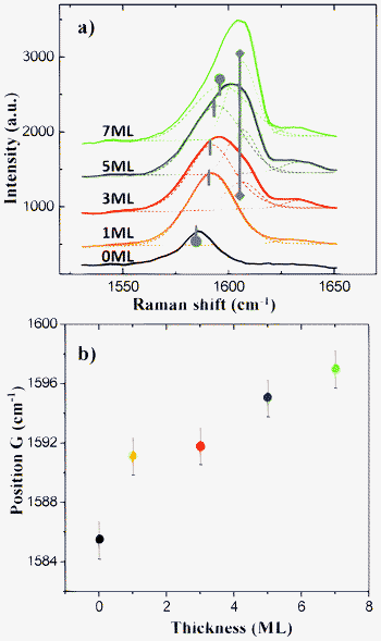 | ||
| Fig. 2 a) The G band of graphene as a function of TCNQ thickness. Spectra taken from 3 ML, 5 ML and 7 ML films were deconvoluted by Gaussian fit into graphene G bands with moving positions (round head bars) and TCNQ CC stretching modes (diamond head bar) with a fixed position at 1605 cm−1. b) Position of G peak as a function of TCNQ coverage. | ||
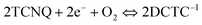
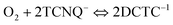
Based on our observation and analysis of the G band of graphene, charge transfer is confirmed in the TCNQ/graphene system, with charge flowing from the graphene. The presence of DCTC−1 is additional evidence of the charge transfer occurring. The capture of electrons by the neutral TCNQ molecules will transform them into anions. However, no spectral bands characteristic of TCNQ anions are observed. It is known that the TCNQ anion readily reacts with oxygen33,34 and water35 in air, and becomes oxidized to form DCTC−1. The DCTC anion has a CO functional group replacing one of the cyano groups. The carbonyl group transforms the symmetric D2h TCNQ parent into an asymmetric DCTC derivative, Fig. 3. The DCTC anion has been detected as an impurity by XPS during the study of the TCNQ anion,26 revealing the chemical reactivity of the TCNQ anion in air. There are several studies on the mechanism by which TCNQ is oxidized to produce the DCTC−1 ion.15,34,36,37 All of them suggest that the reaction has TCNQ anions as the precursors. We thus postulate that charge transfer from graphene to TCNQ produces TCNQ anions that further react with oxygen and results in the formation of DCTC−1. The proposed process of charge transfer and chemical reaction is illustrated in Fig. 3. If one desires to suppress this process, it would be necessary to perform all operations under vacuum or an inert atmosphere and to encapsulate any resulting device prior to exposure to air.
 | ||
| Fig. 3 Proposed process of charge transfer and chemical reaction of the first TCNQ monolayer on graphene. Carbon is black, nitrogen blue, oxygen red and hydrogen is gray. | ||
We interpret the shift in G band with increasing TCNQ load as depicted in Fig. 2(b), and the rapid change in the 2D band position with 1 ML coverage, to indicate charge transfer to less than, or about, one full coverage layer of TCNQ. That is the reason that we only see the DCTC−1 peaks and graphene peaks in Fig. 1(a) (orange curve) but no TCNQ is observed. The shift in the G band with coverage greater than 1 ML is probably due to non-uniform molecular coverage of the graphene surface. One should ask how many electrons are withdrawn for graphene to generate a near monolayer of TCNQ−1, which subsequently reacts with air to form DCTC−1. Unfortunately, the structure of TCNQ on free standing graphene is not known. We can, however, use structures of TCNQ formed on other supports as a guide. On Cu(111), TCNQ adopts a dense structure having 0.89 nm2 per TCNQ.20 On Au(111) it adopts a somewhat more open structure having 0.98 nm2 per TCNQ.21 Using an epitaxial packing motif similar to that of TCNQ on Cu(111) and placing the molecules as densely as the CPK models allow, one arrives at a structure with 0.73 nm2 per molecule coverage Thus, there are at least 30 graphene C atoms per TCNQ molecule in a monolayer. Each C atom in a single layer of graphene need only donate ≤0.03 electrons. With increased loading, more of the exposed graphene surface is covered until electrical equilibrium is established by the negative ions formed, balancing the holes in the graphene layer. The TCNQ deposited on top of the negative ions might exchange charge with the negative ion. However, this is unlikely beyond the second layer since there is a Franck–Condon barrier to this charge exchange and the TCNQ−1 layer may insulate further layers from the graphene. In any case, there is an electrochemical balance that must be maintained. Once the system is exposed to air, the TCNQ ions react to form DCTC−1. One can speculate on the possibility of extra (or a reduced) net charge transfer to graphene resulting from the subsequent chemical reaction. If, for example, one assumes a reversible overall reaction:
 | (1) |
This can be written as the sum of two processes:
 | (2) |
 | (3) |
Then
| ΔG0T = 2ΔG0 + ΔG0O | (4) |
The half cell voltage of the total process, would be
 | (5) |
An obviously interesting experiment would be to measure the Raman spectrum and surface potential of as deposited TCNQ on graphene in UHV and then to continue those measurements upon exposure to O2 and to H2O. Unfortunately, we do not have facilities for performing this experiment.
4. Conclusions
We performed Raman scattering measurements on the species formed when TCNQ is deposited on graphene and on graphite. The product of air exposure of TCNQ/graphene, DCTC−1, was discovered on the graphene samples, revealing an oxidation–reduction chemical reaction between graphene and the first few layers of deposited TCNQ. The same experiment performed with a graphite surface indicated that only physical adsorption occurs to a significant extent. The presence of DCTC−1 is a clear indicator of charge transfer from graphene to TCNQ. Approaching the problem from the graphene side, the variation in the G band of graphene with TCNQ loading also demonstrated charge transfer from graphene to TCNQ. The mechanism of chemical reaction producing DCTC−1 was discussed. This study confirmed that TCNQ can be used to p-dope graphene. It also demonstrates that the graphene to/from adsorbate charge transfer reactions can lead to highly reactive species that undergo subsequent reactions when exposed to air or other chemical environments. Any complete understanding of the graphene charge state and surface charge transport must include a detailed knowledge of the actual final surface species present.Acknowledgements
This material is based upon work supported by the National Science Foundation under grants CHE-1152951, CHE-1112156, and CHE-1058435. We thank Dr Bing Zheng for her assistance with the TOC graphic.References
- X. Wang, X. Li, L. Zhang, Y. Yoon, P. Weber, H. Wang, J. Guo and H. Dai, Science, 2009, 324, 768–771 CrossRef CAS.
- S. Zhou, D. Siegel, A. Fedorov and A. Lanzara, Phys. Rev. Lett., 2008, 101, 086402 CrossRef CAS -1–4.
- V. Kodali, J. Scrimgeour, S. Kim, J. Hankinson, K. Carroll, W. de Heer, C. Berger and J. Curtis, Langmuir, 2010, 27, 863–865 CrossRef.
- S. Saha, R. Chandrakanth, H. Krishnamurthy and U. Waghmare, Phys. Rev. B: Condens. Matter Mater. Phys., 2009, 80, 155414 CrossRef -1–6.
- W. Dou, S. Huang, R. Zhang and C. Lee, J. Chem. Phys., 2011, 134, 094705 CrossRef -1–7.
- H. Huang, S. Chen, X. Gao, W. Chen and A. Wee, ACS Nano, 2009, 3, 3431–3436 CrossRef CAS.
- W. Chen, S. Chen, D. Qi, X. Gao and A. Wee, J. Am. Chem. Soc., 2007, 129, 10418–10422 CrossRef CAS.
- X. Wang, J. Xu, W. Xie and J. Du, J. Phys. Chem., 2011, 115, 7596–7602 CAS.
- J. Gong and Y. Osada, Appl. Phys. Lett., 1992, 61, 2787–2789 CrossRef CAS.
- T. Takenobu, T. Takano, M. Shiraishi, Y. Murakami, M. Ata, H. Kataura, Y. Achiba and Y. Iwasa, Nat. Mater., 2003, 2, 683–688 CrossRef CAS.
- S. Barja, M. Garnica, J. Hinarejos, A. Vazquez de Parga, N. Martin and R. Miranda, Chem. Commun., 2010, 46, 8198–8200 RSC.
- J. Sun, Y. Lu, W. Chen, Y. Feng and A. Wee, Phys. Rev. B: Condens. Matter Mater. Phys., 2010, 81, 155403 CrossRef -1–6.
- M. Khatkale and J. Devlin, J. Chem. Phys., 1979, 70, 1851–1860 CrossRef CAS.
- K. Holczer, G. Mihaly, G. Gruner and A. Janossy, J. Phys. C: Solid State Phys., 1979, 12, 1883–1889 CrossRef CAS.
- K. Nakatani, T. Sakata and H. Tsubomura, Bull. Chem. Soc. Jpn., 1975, 48, 2205–2206 CrossRef CAS.
- X. Ling, L. Xie, Y. Fang, H. Xu, H. Zhang, J. Kong, M. Dresselhaus, J. Zhang and Z. Liu, Nano Lett., 2010, 10, 553–561 CrossRef CAS.
- H. Xu, L. Xie, H. Zhang and J. Zhang, ACS Nano, 2011, 5, 5338–5344 CrossRef CAS.
- Y. Qi, J. Eskelsen, U. Mazur and K. Hipps, Langmuir, 2012, 28, 3489–3493 CrossRef CAS.
- G. Mondio, F. Neri, G. Curro, S. Patane and G. Compagnini, J. Mater. Res., 1993, 8, 2627–2633 CrossRef CAS.
- M. Kamna, T. Graham, J. Love and P. Weiss, Surf. Sci., 1998, 419, 12–23 CrossRef CAS.
- I. Torrente, K. Franke and J. Pascual, Int. J. Mass Spectrom., 2008, 277, 269–273 CrossRef CAS.
- K. Novoselov, A. Geim, S. Morozov, D. Jiang, Y. Zhang, S. Dubonos, I. Grigorieva and A. Firsov, Science, 2004, 306, 666–669 CrossRef CAS.
- Y. Qi, S. H. Rhim, G. F. Sun, M. Weinert and L. Li, Phys. Rev. Lett., 2010, 105, 085502 CrossRef CAS -1–4.
- C. Coletti, C. Riedl, D. Lee, B. Krauss, L. Patthey, K. Klitzing, J. Smet and U. Starke, Phys. Rev. B: Condens. Matter Mater. Phys., 2010, 81, 235401 CrossRef -1–8.
- A. Pawlukojc, I. Natkaniec, G. Bator, L. Sobczyk and E. Grech, Chem. Phys. Lett., 2003, 378, 665–672 CrossRef CAS.
- M. Harris, J. Joagland, U. Mazur and K. Hipps, Vib. Spectrosc., 1995, 9, 273–277 CrossRef CAS.
- R. Nemanich and S. Solin, Phys. Rev. B, 1979, 20, 392–401 CrossRef CAS.
- A. Das, S. Pisana, B. Chakraborty, S. Piscanec, S. Saha, U. Waghmare, K. Novoselov, H. Krishnamurthy, A. Geim, A. Ferrari and A. Sood, Nat. Nanotechnol., 2008, 3, 210–215 CrossRef CAS.
- L. Pietronero and S. Strassler, Phys. Rev. Lett., 1981, 47, 593–596 CrossRef CAS.
- R. Voggu, B. Das, C. Rout and C. Rao, J. Phys.: Condens. Matter, 2008, 20, 472204 CrossRef -1–5.
- H. Medina, Y. Lin, D. Obergfell and P. Chiu, Adv. Funct. Mater., 2011, 21, 2687–2692 CrossRef CAS.
- Z. Ni, Y. Wang, T. Yu and Z. Shen, Nano Res., 2008, 1, 273–291 CrossRef CAS.
- J. S. Miller, A. H. Reis, E. Gebert, J. Ritsko, W. Salaneck, L. Kovnat, T. Cape and R. P. Van Duyne, J. Am. Chem. Soc., 1979, 101, 7111–7113 CrossRef CAS.
- M. Suchanski and R. Van Duyne, J. Am. Chem. Soc., 1976, 98, 250–252 CrossRef CAS.
- K. Mizoguchi, S. Tsuji, E. Tsuchida and I. Shinohara, Nippon Kagaku Kaishi, 1977, 8, 395–399 CrossRef.
- M. Grossel, A. Duke, D. Hibbert, I. Lewis, E. Seddon, P. Horton and S. Weston, Chem. Mater., 2000, 12, 2319–2323 CrossRef CAS.
- K. Mizoguchi, S. Tsuji, E. Tsuchida and I. Shinohara, J. Polym. Sci., 1978, 16, 3260–3274 Search PubMed.
| This journal is © The Royal Society of Chemistry 2012 |