In depth analysis of complex interfacial processes: in situ electrochemical characterization of deposition of atomic layers of Cu, Pb and Te on Pd electrodes
Minghua
Huang†
,
John B.
Henry†
,
Philippe
Fortgang
,
Jörg
Henig
,
Nicolas
Plumeré
and
Aliaksandr S.
Bandarenka
*
Center for Electrochemical Sciences – CES, Ruhr-Universität Bochum, Universitätsstr., 150, D-44780 Bochum, Germany. E-mail: aliaksandr.bandarenka@rub.de; Tel: +49 (0)234 32 29433
First published on 17th September 2012
Abstract
A combination of cyclic voltammetry, electrogravimetry, and electrochemical impedance spectroscopy has been used to characterize, in situ, the underpotential deposition (UPD) of atomic layers of Cu, Pb and Te on Pd electrode surfaces. This approach provides co-adsorption and competitive adsorption of anions to be measured and quantified during the UPD processes, highlighting the complex competitive processes that can e.g. hinder the design of new catalysts. The formed Cu, Pb and Te atomic layers on the Pd electrode showed no evidence of anion co-adsorption or surface alloying effects, which indicates that these systems, when formed in a perchlorate medium, could act as building blocks for catalysts. The mode of deposition was found to vary greatly for each overlayer. Cu was found to form a compact monolayer on the Pd surface, while Te formed a bilayer structure on the Pd surface, of which ∼1/4 of a monolayer was found to be irreversibly adsorbed. The formation of Pb overlayers was complicated by background UPD of hydrogen and its absorption to the underlying Pd substrate. While perchloric acid media are suitable for the formation of the overlayer, catalytic application of the formed Pb-layers would require a higher pH to negate such processes.
1 Introduction
The rational design of efficient electrocatalytic systems has attracted considerable attention in many rapidly expanding technological fields, such as the development of alternative energy sources,1,2 biosensors,3,4 and electrochemical synthesis.5,6 For electrochemical reactions, the surface structure (both geometric and electronic) of an electrocatalyst is crucial to establish optimal catalytic activity. Tuning the catalytic activity, therefore, can be achieved through engineering the electronic structure of the electrode surface by modification of the surface structure and/or composition.7Electrochemistry provides a fine precision tool for controllable modification of the structure and composition of the electrode surfaces through underpotential deposition (UPD), where the deposition of a single monolayer or submonolayer amounts of foreign metals and non-metals occurs at potentials that are more anodic than the potential of bulk 3D phase growth.8 Electrochemistry, particularly UPD, provides the ideal tools for the creation of new catalysts as the judicious choice of electrode potential can allow fine control over surface coverage and, in some cases, structure. Such fine tuning can allow surfaces to be tailored for specific applications.
UPD has attracted particular interest due to its applicability in tailoring diverse surface structures and properties, such as electrocrystallization, thin films, sensors and electrocatalysis. Electrocatalytic properties have been examined extensively in a varied range of UPD systems to catalyze a number of important reactions, for example, nitrate reduction,9 oxidation of organic compounds,10,11 and particularly O2 reduction12,13 and H2 evolution,14 which are vital for fuel cells. As well as forming active catalyst surfaces, UPD formed monolayers can also act as building blocks for further surface modification to fit the electrode surface for a particular electrochemical reaction, either through further UPD of a third metal15 or the formation of surface alloys and near-surface alloys (Fig. 1).16
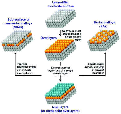 | ||
| Fig. 1 A schematic representation of strategies involving UPD to optimize electrode surface reactivity and electrocatalytic activity. | ||
To better understand the catalytic activity and fully exploit potential applications in electrocatalysis, it is necessary to address the kinetics and structural aspects of UPD on various substrates to gain a deeper understanding of the dynamic processes that occur at the electrode/electrolyte interface. Conventional voltammetric techniques and impedance measurements have been used to characterize UPD systems and have provided valuable information on the steady state systems.17 However, such techniques when used in isolation can be limited in their ability to characterize non-stationary aspects of UPD, such as surface alloying, lateral interactions in adsorbate layers, electrode surface oxidation and surface reconstruction. Thus, there remains a challenge to develop new approaches and methodologies to monitor, in situ, the non-stationary characteristics of UPD systems. Ideally such methodologies should use several independent parameters or, alternatively, use so-called “hyphenated techniques”, to allow the acquisition of the maximum amount of independent and self-consistent data to enable the electrode/electrolyte interface dynamics to be characterized.
Very recently, we reported on a complementary in situ technique that simultaneously acquires potentiodynamic electrochemical impedance and gravimetric data in a single cyclic potential scan.18 This technique has already shown its value in characterizing a range of complex non-stationary electrochemical phenomena, such as UPD of Ag and Cu on Au and Pt substrates,18 and electrocatalysis on a hybrid substrate19 and also intercalation of Cu into a Te electrode.20 The development of this technique shows particular promise for elucidating physical models of electrode/electrolyte interfaces, and hence, provides a deeper physical insight into non-stationary systems. In this work, we demonstrate how this technique can be applied to characterize the electrode/electrolyte interface during complex UPD processes on Pd electrodes where the deposition can be complicated by a variety of competing processes, selecting the representative systems of Cu, Pb, and Te on polycrystalline Pd electrodes.
The choice of UPD systems is based on the following considerations. First, most studies of UPD have focused on deposition on Au, Pt and Ag electrodes.8 While Pd is the most Pt-like metal and a relatively abundant resource, UPD on Pd electrodes has received considerably less attention.21,22Model experiments are normally performed on single crystal electrodes. Such experiments are an invaluable source of information on fundamental electrochemical reactions as they allow the characterisation of electrochemical processes at a single crystal facet. Reactions at polycrystalline electrodes, which contain a range of facets at the electrode surface, can then often be interpreted as a combination of the processes that occur at single crystal facets. In this study we therefore focus on polycrystalline electrodes as these electrodes are currently of interest for commercial applications. It is hoped that the results presented within this paper can advance the consideration of electrode processes on Pd substrates and work in conjunction with single crystal experiments to enhance the fundamental knowledge of these processes.
While Cu UPD on Pd has been the subject of recent studies,23,24 particularly on Pd(111), to the best of our knowledge Pb and Te UPD on Pd have not been electrochemically characterized, although Pb UPD has been used to tune a Pd surface towards the catalytic electrooxidation of formaldehyde.21 Most importantly, these systems are of clear interest for electrocatalytic applications; Cu and Pb atomic layers on many substrates are known to activate NO3− reduction,9 while Te layers on Pt can catalyze CO oxidation.25 Due to the similar properties of Pt and Pd substrates it is reasonable to assume that methods that have improved catalytic activities in Pt-based systems can be extended to Pd-based systems, while the lower cost of Pd may make such systems more economically viable. Achieving a deeper understanding of such UPD systems may, therefore, be significant in advancing catalytic applications.
Here, our particular goal is to analyze the electrolyte/electrode interface status during UPD of Cu, Pb and Te, which should allow an evaluation of whether possible anion co-adsorption, competitive adsorption, or spontaneous surface alloying effects occur. These processes are normally not desirable in electrocatalysis as specific adsorption of electrolyte components can commonly poison active centers while spontaneous surface alloying may limit long-term catalyst stability. The absence of anion specific adsorption would also secure further thermal treatment of electrodes from unpredictable high-temperature chemical interactions at the surface during the preparation of surface and near-surface alloys (Fig. 1).
2 Experimental section
2.1 Chemicals
Siemens UltraClear water was used to prepare all solutions (0.055 μS cm−1, TOC content < 1 ppb). Copper(II) oxide (99.9999%, metal basis, Aldrich) Pb(ClO4)2·xH2O (≥99.995%, Fluka), TeO2 (99.995%, Aldrich) were used to prepare Cu2+, Pb2+ and HTeO2+ solutions. HClO4 (Aldrich, TraceSelect Ultra), 96% H2SO4 (Merck, Suprapur) and 30% H2O2 (Merck, Suprapur) were used to prepare a “piranha” solution with a 3![[thin space (1/6-em)]](https://www.rsc.org/images/entities/char_2009.gif) :1 solution ratio. All glassware used in this work was cleaned for 12 h with this solution (Caution: since piranha solution reacts violently with many organic compounds, extreme care must be taken). To remove sulfate ions, multiple heating, ultrasonic treatments and rinsing with Siemens UltraClear water were used.
:1 solution ratio. All glassware used in this work was cleaned for 12 h with this solution (Caution: since piranha solution reacts violently with many organic compounds, extreme care must be taken). To remove sulfate ions, multiple heating, ultrasonic treatments and rinsing with Siemens UltraClear water were used.
2.2 Deposition of Cu, Pb and Te on polycrystalline Pd electrode
Electrochemical studies were carried out with a SP-300 potentiostat (Bio-logic, France) in a special electrochemical cell which allows complete degassing of the system and electrolyte prior to experiments (Fig. 2).18,19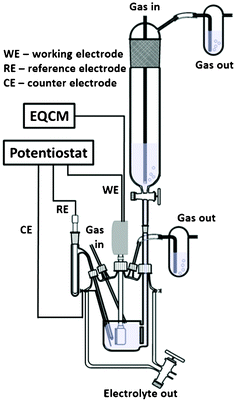 | ||
| Fig. 2 A schematic drawing of the electrochemical cell | ||
Au foil (Goodfellow) of high surface area was used as the counter electrode (CE) and a mercury–mercury sulfate (MMS) reference electrode (RE) (commercial electrode supplied by Schott, Hg/Hg2SO4/K2SO4 (sat'd), 0.65 V vs. normal hydrogen electrode (NHE), kept in a separate compartment and separated from the working solution with a ceramic insert) were used in all electrochemical experiments.
All potentials are reported with respect to the MMS reference electrode. An AT-cut Au quartz crystal wafer (5 MHz, 1′′ diameter, Stanford Research Systems, USA) sputtered in house with a Pd layer was used as the working electrode (WE) (Sgeom = 1.37 cm2, this value is used to normalize all relevant parameters). The sputtered layer was created using a conventional photolithographic technique.
The commercial Au/quartz crystal electrode was first cleaned with acetone, isopropanol and dried under a nitrogen flow. A 2 μm layer of photosensitive resin AZ5214E (Clariant, USA) was then spin-coated on the electrode at 4600 rpm for 60 s and then baked at 100 °C for 60 s. After cooling (3 min), the resin was exposed to UV light (λ = 360 nm for 6 s) through a mask to transfer the desired pattern. A soft baking (120 °C for 120 s) was followed by UV exposure (λ = 360 nm for 20 s) without the optical mask to invert the polarity of the previously exposed image. The sample was then developed in AZ MIF 726 (Clariant, USA) for 30 s then rinsed in deionized water and dried in a nitrogen stream. This process exposed only the area where the Pd should be sputtered. The Pd sputtering from an elemental target of palladium was performed with an ultra-high vacuum combinatorial magnetron sputter system (DCA, Finland) with a deposition rate of 11 nm min−1 until a Pd layer thickness of ∼100 nm was obtained.
AFM data for the prepared Pd WE are shown in Fig. 3a. AFM measurements were carried out on a JPK NanoWizard 3 in tapping mode using AppNano ACTA cantilevers. A standard calibration procedure involving bulk deposition of Cu was performed to ensure linearity of the electrochemical quartz crystal microbalance (EQCM) frequency shift of the modified Pd/Au/quartz electrode with an increase of the deposited mass, ensuring the modified electrode still responded as expected in accordance with the Sauerbrey equation.
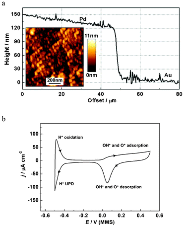 | ||
| Fig. 3 Characterization of the Pd electrode: (a) cross section of a Pd–Au edge (without tilt correction) for a special sample prepared to quantify the Pd layer thickness (an AFM image of the Pd surface is shown in the inset); (b) the characteristic cyclic voltammogram for the Pd electrode in 0.1 M HClO4, dE/dt = 50 mV s−1. | ||
The EQCM-crystal holder, a commercial SRS Kynar holder with a Viton O-ring, was repeatedly cleaned overnight in 30% H2O2 with a “dummy” quartz crystal loaded. Before experiments, the Pd electrode was electrochemically cleaned in 0.1 M HClO4 until voltammetric characteristics for a clean Pd electrode were obtained (Fig. 3b). It is noted that the asymmetric double layer region of the CV may be due to a delayed reduction of the adsorbed O and OH. Varied oxidation potential ranges have previously been observed in other Pd systems.26 The cathodic current observed below −0.4 V is attributed to hydrogen UPD and absorption processes, which occur concurrently, which also agrees well with other previous reports.26,27 Therefore, the charge of hydrogen UPD cannot be used to simply calculate the electrochemical surface area of the Pd electrode due to the interference of the hydrogen absorption process. The roughness factor, defined as the ratio of electrochemical surface area over geometric surface area, was estimated to be ca. 1.1 with a method that considers the reduction of a fully covered Pd(OH)2 layer.26,27 This indicates a relatively even surface, in good agreement with AFM analysis of the surface.
Solutions of 1 mM Cu2+ + 0.1 M HClO4, 1 mM Pb2+ + 0.1 M HClO4, and 0.5 mM HTeO2+ + 0.1 M HClO4 were used for the UPD of Cu, Pb, and Te on Pd, respectively. Solutions were deaerated for at least 20 min with a high purity Ar stream (Air Liquid, 5.0, Germany, supplied using Swagelok® stainless steel tubing), with all experiments performed under a constant Ar-atmosphere.
For the electrochemical impedance spectroscopy (EIS) measurements, a capacitive shunt was connected between the RE and CE to minimize artifacts caused by the potentiostat at high frequencies, with the value of capacitance selected empirically through a series of calibration experiments. The ac probing frequency range was 30 kHz–10 Hz, with lower frequencies avoided to maintain a reasonable potential scan rate and minimize possible random contamination during the course of the experiments. The ac probing signal amplitude was 10 mV. The potential was then scanned stepwise similar to experimental protocols reported elsewhere.18,28–31 The EIS spectra analysis, including linear and logarithmic Kramers–Kronig tests, was performed with the EIS Spectrum Analyzer software.32,33 The quality of the fitting and modelling was ensured by analysis of the estimated errors of individual parameter values and the root-mean-square deviation of the fitted curves to the experimental data with deviations of more than 2% being viewed as unacceptable. A QCM200 quartz crystal microbalance (Stanford Research Systems, USA) was used to measure the mass response of the WE. During combined EQCM-EIS experiments, the EQCM and EIS measurements were synchronized but run independently.
3 Results and discussions
3.1 Theoretical considerations for EIS
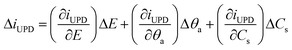
EIS probes the electrochemical interface with small (∼10 mV) ac signals normally within frequency ranges from a few MHz to μHz, with the appropriate range selection dependent on the system properties. The analysis of impedance data involves finding a physical model (which can either be expressed in terms of fundamental equations or as equivalent electric circuits, EECs) of the electrochemical interface and establishing parameters by fitting of the EIS spectra to the model.Here we present theoretical considerations for the elucidation of physical models for EIS of the UPD of metal atomic layers. When small ac perturbation signals are applied to a system where single-stage UPD occurs, the Faradaic current, iUPD, the adatom coverage, θa, and surface concentrations, Cs, of the electroactive species oscillate around quasi-steady-state values. The linear part of the response assigned to the UPD process can be written as:
 | (1) |
 | (2) |
| Zdl = C′dl−1(jω)−n | (3) |
At steady state, for a “voltammetrically reversible” UPD process, the dc current should be zero, where ω → 0. The adsorption model given by eqn (2) models this fact well. This model does allow a dc current to flow under non-steady state conditions, i.e. during a potentiodynamic scan, enabling charging of the adsorption capacitance. However, in the absence of diffusion limitations, analysis of eqn (1) allows us to exclude the Warburg impedance.35,37,38 The ability to distinguish between the double layer and the adsorption capacitances is dependent on the charge transfer resistance when there are no diffusion limitations. Alternatively, for two simultaneous adsorption processes, one with diffusion limitations and one without, different time constants for each adsorption allow separation of each of them in EIS experiments.37,38 However, for slow irreversible adsorptions, contributions of the Δθa and ΔCs in eqn (1) can be small, leaving only the charge transfer resistance to model the Faradaic impedance.
The measurement results and a priori knowledge of the system provide the basis for the selection of an appropriate physical model for the EIS spectra fitting. Independent knowledge obtained via EQCM measurements is vital to acquire relevant pre-knowledge and adds support to the modelling process, allowing the elucidation of a physical model for the polycrystalline electrode.
3.2 Deposition of Cu atomic layers on Pd
Based on the fact that a Cu atomic layer on Pd is well known to be an active catalyst for a number of important catalytic reactions, such as nitrate reduction,39 and can also form a sacrificial layer to create an active Pt catalytic monolayer on bulk Pd for the O2 reduction reaction,40 we selected Cu UPD on a Pd electrode as a model system to investigate different aspects of the atomic layer formation using EQCM-EIS.In this work, we use HClO4 as an electrolyte, as ClO4− ions are not usually specifically co-adsorbed at electrode surfaces in electrochemical studies. Fig. 4 shows the cyclic voltammograms (CVs) for Cu UPD on a Pd electrode in 0.1 M HClO4. A series of broad adsorption–desorption peaks are observed before bulk Cu deposition occurs, which agree with previously reported observations.41 It is worth noting that when compared to Cu UPD on Pt the CV of the Cu UPD on Pd shows a higher degree of voltammetric reversibility,18 illustrated by the smaller reductive and oxidative peak separations. Such differences in voltammetric features appear counterintuitive considering that Pt and Pd electrodes often demonstrate similar properties.
 | ||
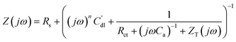
| Fig. 4 Cu UPD on polycrystalline Pd: (a) cyclic voltammograms taken during continuous cycling of the electrode potential (dE/dt = 50 mV s−1) and after the potential was held at −0.43 V for 2 min; (b) electrode mass change during the Cu UPD, cathodic treatment at −0.43 V, and subsequent Cu atomic layer oxidation (anodic scan); (c) the measured electrode mass change as a function of the voltammetric charge during continuous cycling of the electrode potential. | ||
A charge value of ∼280 μC cm−2 can be determined from the anodic part of the voltammogram when continuous potential cycling is performed (dotted line in Fig. 4a). However, if the potential is held at the cathodic limit of −0.43 V for 2 min or longer, a stable anodic charge of ∼400 μC cm−2 is obtained (solid line in Fig. 4a). This implies that while Cu UPD on Pd is, in general, a quasi-reversible process, the kinetics of the final stages of UPD is slow. Considering the theoretical charge value for Cu UPD on Pd (111) surface (assuming that this facet normally dominates at the surface of polycrystalline Pd42) is around 480 μC cm−2, it is clear that the value observed with CV is lower than this, even following a relatively long cathodic treatment at −0.43 V. If the electrode is held at −0.44 V, bulk deposition of Cu begins; and the corresponding Cu anodic peak increases due to the oxidation of bulk Cu, which indicates that the selected potential range from 0 to −0.43 V (MMS) covers the entire UPD range.
Fig. 4b shows the mass change in the Cu adsorption and desorption processes, if the cathodic treatment of 2 min at −0.43 V is used. It can be observed that after holding the potential at the cathodic limit for 2 min, the mass appears to reach a stable value of around 140 ng cm−2. The expected mass change, assuming formation of a compact monolayer with 1 Cu atom for each Pd atom, for an equivalent Pd(111) crystal would be ∼158 ng cm−2. This difference between observed and theoretical values can again be explained by the slow Cu UPD kinetics at the final stages of the process,18 which prevents the formation of a complete monolayer on the timescale of the experiment. While the monolayer formed appears incomplete, it is possible to calculate the molar weight of the adsorbate through consideration of the observed anodic charge (∼400 μC cm−2) and the deposited mass on the electrode (∼140 ng cm−2). Such an analysis gives an adsorbate molar weight of ∼68 g mol−1. Additionally, plotting the measured electrode mass change as a function of the voltammetric charge reveals linear behaviour with a constant slope corresponding to the apparent molar weight being ∼67 g mol−1 (Fig. 4c), assuming a two-electron process. These apparent molar weights are in good agreement with the expected Cu molar weight of 63.5 g mol−1. This implies that Cu UPD on Pd occurs without significant specific co-adsorption of the “bulky” anions from the electrolyte, which is similar to the observed behaviour of Cu UPD on Pt.18 However, co-adsorption of small amounts of OH*, cannot be completely excluded.
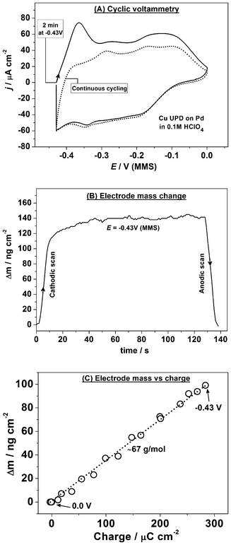
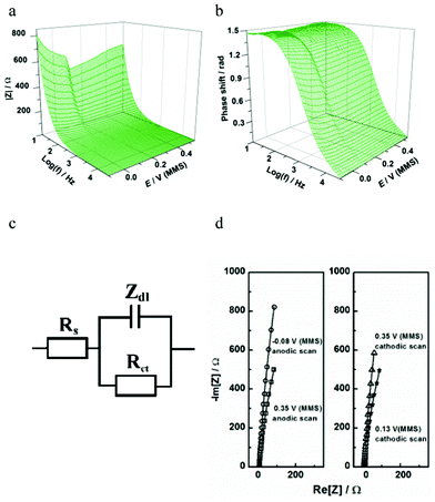
Fig. 5a and b show the extended Bode plots of the impedance spectra (|Z| and phase shift, respectively, as functions of the potential E and ac frequency) acquired in a staircase cathodic scan for Cu UPD on Pd. This impedance dataset is a collection of 2D impedance spectra taken simultaneously with the EQCM data (Fig. 6), as defined in the experimental section. While the raw data-set appears to show a complicated adsorption process, the impedance data combined with the EQCM and CV data can be used to elucidate a physical model of the electrode/electrolyte interface at different potentials according to the procedure described elsewhere.18
 | ||
| Fig. 5 Characterization of Cu UPD on Pd using impedance spectroscopy: (a,b) extended Bode plots of the impedance spectra (explained in the text) obtained in the cathodic scan (dE/dt = 0.3 mV s−1); (c) a physical model of the electrode/electrolyte interface in terms of equivalent electric circuit (Rs and Rct are the electrolyte and charge transfer resistances, respectively; Ca is the Cu adsorption capacitance, Zw and Zdl are the diffusion and double layer impedances, respectively); (d) examples of the experimental data (open symbols) and the fitting results (solid lines) at some selected electrode potentials. | ||
 | ||
| Fig. 6 Electrode mass change, the EQCM resonance resistance, C′dl(E), adsorption capacitance and the inverse of the charge transfer resistance variations during Cu UPD on the polycrystalline Pd. | ||
The classic model for reversible adsorption (shown in Fig. 5c and discussed in section 3.1) was found to give the best fit to the impedance data characterizing the Cu atomic layer deposition/oxidation on Pd both in the cathodic and anodic scans. However, the contribution from the diffusion Warburg impedance ZW appeared to be small, especially at the initial stages of Cu UPD (this element is marked with a dotted contour in Fig. 5c). No additional components related to a co-adsorption of other electrolyte components appear to be necessary, which is consistent with the EQCM data. Additionally, the appearance of the adsorption capacitance Ca is in agreement with the fact that voltammetry of Cu UPD on Pd discloses some reversible adsorption and desorption of Cu. Fig. 5d demonstrates examples of fitting to the proposed model for a few selected 2D impedance spectra. The model in Fig. 5c fits well to the experimental data with appropriately low errors for individual parameters in the regions where these parameters have physical meaning.
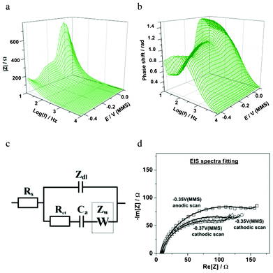
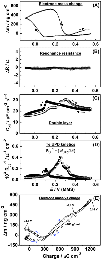
Fig. 6 summarizes some essential EQCM-EIS results for the in situ characterization of Cu UPD on Pd. As shown in Fig. 6a, Cu deposition and desorption are clearly observed through the variation of the electrode mass change Δm(E) during the slow staircase potential scan. The mass observed at the end of the slow Cu deposition (∼165 ng cm−2) is clearly larger than that observed by the previous voltammetric experiments (∼140 ng cm−2), but in good agreement with the theoretical value for a compact Cu monolayer on Pd (111) (∼158 ng cm−2). This again highlights the peculiarities of the Cu UPD kinetics, with the much slower scan rate used in the EIS-EQCM experiment allowing the Cu to form a more compact layer on the Pd surface. Additionally, the electrode mass variation confirms that there is no significant co-adsorption of e.g. perchlorate anions during the Cu UPD process on Pd. These results are similar to those observed for the UPD of Cu on Pt.18 As well as mass change, Δm, EQCM also measures the series resonance resistance, ΔR, which corresponds to the oscillation energy dissipation from growing structures and from the medium in contact with the crystal. ΔR also changes with the viscosity or elasticity of the material (film or liquid) in contact with the crystal surface. Therefore, ΔR can be used as an independent indicator of e.g. viscosity change at the electrode/electrolyte interface during the electrochemical deposition.18 It can be noted that ΔR is largely constant (Fig. 6b) in both the cathodic and anodic scans, which suggests that the adsorbate is rigidly attached to the electrode surface and the surface roughening effects are likely small.18 Taking into account the Δm(E) profiles (Fig. 4b and 6a) and similar observations for Cu UPD on Pt, this provides an indication that no significant surface alloying effects between the deposited Cu adatoms and the underlying Pd surface are likely in this potential window. However, further investigation is needed to completely verify this.
Fig. 6c shows the variation of the equivalent circuit parameter C′dl with the electrode potential in the Cu UPD region. C′dl is proportional to the double layer capacitance and in many cases sensitive to adsorption processes, 2D phase transitions and new phase growth. As can be seen in Fig. 6c, the variation of C′dl on the potential follows the same trend as Δm(E), and exhibits slightly different interface status in the cathodic and anodic scans. At the final stage of the Cu UPD a 3-fold increase in the C′dl values is observed, which is most likely due to the formation of a more compact double layer. However, some background H-UPD and hydrogen absorption on Pd may also contribute to the apparent C′dl values.
The variation of the adsorption capacitance with the electrode potential, Ca(E), is shown in the potential regions relevant for Cu UPD (Fig. 6d). The appearance of Ca in the model that describes the Cu UPD is expected when the high degree of reversibility of this UPD process, as disclosed by CV measurements, is taken into account. Considering the physical meaning of the Ca, (Ca = − qa(∂θa/∂E)), which is caused by oscillations of the Cuad surface coverage during the ac probing, it is possible to estimate the fraction of Cuad that can be reversibly adsorbed/desorbed during the ac probing, by calculating the ratio Δqa/Δmtotal. Using the Δm(E) dataset yields an estimation of these values between Δqa/Δmtotal ∼ 0.15 and Δqa/Δmtotal ∼ 0.2. These values also depend on the scan direction (Fig. 6d). In addition, according to the inverse charge transfer resistance dependences, Rct(E), the maximum Cu deposition rate is at around −0.37 V (Fig. 6e), which is consistent with the corresponding mass changes Δm(E).
The key features to note for the UPD of Cu on Pd are: (i) slow Cu UPD kinetics in the final stages, (ii) no significant anions co-adsorption, and (iii) no spontaneous surface alloy effects. The latter two features may be beneficial to tailor the surface for catalytic applications, particularly the formation of near-surface alloy catalysts where formation of an uncontaminated UPD layer is essential (Fig. 1). Specific anion co-adsorption and surface alloying would inhibit the active sites of catalysts and impair the long-term stability of catalysts. The absence of these processes in Cu monolayers deposited on Pd suggests that these layers could provide promising materials for catalytic applications.
3.3 Deposition of Pb atomic layers on Pd
Having established that the combined EIS-EQCM technique can characterize the electrode/electrolyte interface in situ during the UPD of Cu on Pd, it was decided to further study the interface during potentially more complex UPD processes that could also form the basis for catalyst systems. Since monolayer and submonolayer amounts of Pb on noble metal electrodes have shown promise for important electrocatalytic processes, such as the reduction of H2O2 to H2O,43 Pb UPD on Pd was selected as a system for study as a promising candidate for catalysis that may present a more complex electrode/electrolyte interface during the UPD process.Fig. 7a (solid line) displays the CV obtained for Pb UPD on Pd in 0.1 M HClO4. The voltammetrically irreversible nature of the Pb UPD process on Pd is evident through the large separation of the reductive and oxidative peaks, as well as the broadness of the anodic stripping peak. At potentials more positive than 0 V, the onset of OH* and O* adsorption at the Pd electrode can be observed.
 | ||
| Fig. 7 (a) The cyclic voltammogram and corresponding massogram for Pb UPD on the polycrystalline Pd (dE/dt = 50 mV s−1) and (b) the corresponding plot showing electrode mass change as a function of the voltammetric charge. | ||
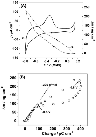
Compared to the CV of the Pd electrode in 0.1 M HClO4 (Fig. 3b), it can be seen that the deposition of Pb on Pd severely suppresses H-UPD and delays H absorption. However, it is difficult to determine the precise extent of this suppression by cyclic voltammetry alone. The charge calculated for the anodic part of the voltammogram was found to be around 400 μC cm−2, which is higher than the expected value for a Pb monolayer on Pd(111), correcting for the larger atomic radius of Pb vs. Pd. The discrepancy in charge is likely due to possible concurrent H-UPD and H absorption at some facets where the Pb atomic layer is defective or Pb does not poison all the H-UPD active sites.
The dotted line in Fig. 7a shows the mass change of the Pd electrode during the Pb UPD process. Due to the possible overlap of hydrogen UPD and absorption processes near the cathodic limit of the Pb UPD process, it is problematic to precisely quantify the charge for Pb UPD. Therefore, it is difficult to calculate the apparent molar weight for the adsorbate using voltammetric data and EQCM data. From the massogram, the mass change at −0.8 V (MMS) is determined to be ∼240 ng cm−2. This is lower than the theoretical values of around 510 ng cm−2 for a hypothetical 1:1 Pb monolayer on well-ordered Pd(111) crystals, the apparent Pb:Pd ratio in the resultant layer is therefore l:2. This difference can be probably explained by the large difference in size of the Pb atoms forming the overlayer and the underlying Pd atoms (∼0.137 nm and ∼0.175 nm for Pd and Pb, respectively). This may mean that surface defects of the Pd electrode, which favor hydrogen absorption, become significant. In addition, it is noted that previous reports of crystal strain affecting EQCM response with high quantities of absorbed hydrogen in Pd44 are unlikely to be observed in this case, as the amount of hydrogen absorbed during these experiments is very low in comparison.
Fig. 7b shows the electrode mass change as a function of the voltammetric charge and provides additional evidence for hydrogen absorption at lower potentials. While the linear slope in Fig. 7b corresponds to the apparent molar weight for the deposited adsorbate being ∼220 g mol−1 (which is reasonably close to the expected value for Pb), at potentials lower than ∼0.5 V the apparent molar weight is drastically decreased. The latter fact can be explained only by taking into account hydrogen absorption, which occurs in parallel with lead deposition.
Fig. 8 presents the EIS spectra taken during Pb UPD on Pd. The best-fit physical model in this case contains two branches in parallel to the double layer impedance (Fig. 8c). We postulate that the slow Pb UPD process is described by the R–W combination similar to other irreversible UPD processes.18,29 The contribution of these two elements is significant exactly in the range where the Pb UPD takes place. A contribution from another (background) process, which can be described in the model with a R–C combination (marked with a dotted line in Fig. 8c), becomes significant only at larger cathodic potentials where H- UPD is possible (Fig. 8d) at the bare Pd surface without Pb2+ in the solution. This suggests that this R–C combination models the H-UPD process, which is entirely consistent with the CV and EQCM results. Notably, the R–C combination is found to describe H-UPD at many surfaces including Pt. These results highlight the greater insight allowed by EIS methods over simple CV. While CV indicates that H-UPD on Pd is largely suppressed (Fig. 7a), the requirement of an additional adsorption process in the model to characterize the electrode/electrolyte interface additionally suggests that the H-UPD process is not completely inhibited by Pb UPD on Pd (Fig. 8c). Therefore, our voltammetric, EQCM and EIS analysis corroborates the hypothesis that the concurrent background H-UPD process influences the Pb UPD process.
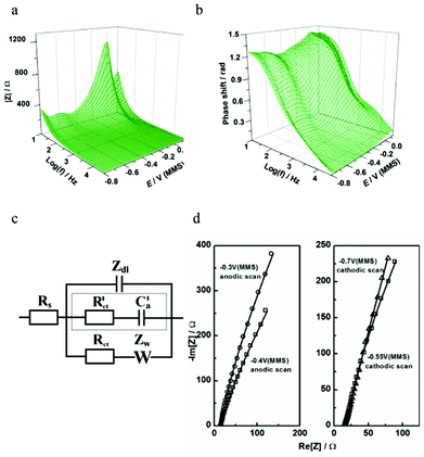 | ||
| Fig. 8 Characterization of Pb UPD on Pd using impedance spectroscopy: (a,b) extended Bode plots of the impedance spectra obtained in the cathodic scan; (c) physical model of electrode/electrolyte interface in terms of an equivalent electric circuit; (d) examples of the experimental data (open symbols) and the fitting results (solid lines) at some selected electrode potentials. | ||
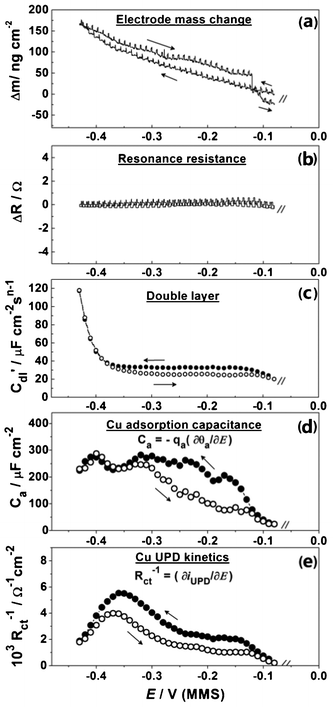
Some essential EQCM-EIS data for the in situ investigation of Pb UPD on Pd are presented in Fig. 9. Fig. 9a shows the dependencies of the electrode mass Δm on the electrode potential E during the slow EQCM-EIS measurement. The observed mass change at −0.8 V (MMS) is ∼250 ng cm−2 (Fig. 9a); we associate this change mainly with the Pb deposition, although background H absorption may also contribute. We also suggest that the influence of the specific anion co-adsorption is unlikely, once the EIS analysis and the data presented in Fig. 7b are taken into account. The larger measured mass change compared to that obtained together with the voltammetric data suggests that the slow potential scan rate allows the formation of a more compact Pb atomic layer. Considering that the measured mass change of the Pd electrode is twice as low as would be expected for a hypothetical 1:1 Pb monolayer on palladium, we hypothesize that Pb forms an atomic layer with a 1:2 ratio with the underlying Pd layer. Note, that this ratio is derived from comparison of expected and measured electrode mass changes.
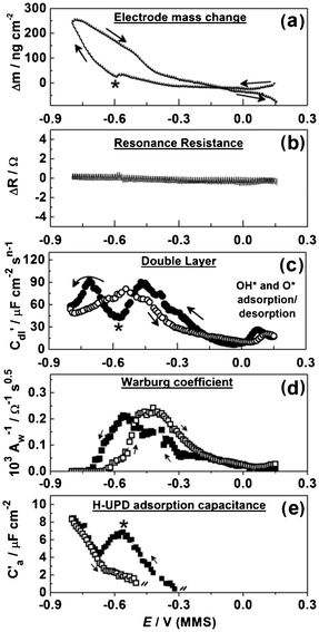 | ||
| Fig. 9 Electrode mass change, the EQCM resonance resistance, C′dl(E), Aw−1(E) and adsorption capacitance of H-UPD variations during Pb UPD on polycrystalline Pd (dE/dt = 0.3 mV s−1). | ||
Fig. 9b shows that, similar to Cu UPD on Pd, ΔR values can be seen to be largely unchanged during the cathodic and anodic scans, which suggests that spontaneous surface alloying or roughening effects are small18 during the adsorption/desorption of Pb. This result indicates that no spontaneous surface alloying effects occur between Pb adatoms and the Pd substrate, which is crucial to the long-term stability of potential catalysts.
The variation of C′dl with the electrode potential during Pb UPD on Pd is shown in Fig. 9c. The variation between the C′dl response on the cathodic and anodic scans highlights the aforementioned irreversibility of the Pb UPD process on Pd. The C′dl(E) and Δm(E) additionally disclose the Pb UPD as a two-stage process with the characteristic point at around −0.6 V (denoted with stars in Fig. 9). Notably, the massogram recorded simultaneously with CV (Fig. 7) also displays a similar change in gradient at −0.6 V.
Fig. 9d presents the dependence of the inverse Warburg coefficient on the potential AW−1(E) ∝ (∂Cs/∂E), where Cs is the surface concentration of the electroactive species Pb2+. It was not possible to calculate the apparent rate coefficient from the AW(E) and Rct(E) dependences18 as the individual errors of the Rct values (not shown) estimated from the fitting procedure were too high for accurate calculation of this kinetic parameter. Being dependent on the Pb fractional coverage θa, AW−1(E) values approach zero at the cathodic potentials where the Pb atomic layer is completed. Anodic and cathodic peaks of the AW−1(E) dependences are separated, which is consistent with the Δm(E) dependences.
Fig. 9e shows the adsorption capacitance for the concurrent H-UPD process. It is clear from the cathodic scan that the peak in H-UPD capacitance occurs at the same point as the change in the two-stage process of Pb UPD, −0.6 V. This is likely due to the greater surface coverage of Pb on the electrode surface impeding further H-UPD. Apart from H-UPD, there is no other specific co-adsorption of anions, which indicates that Pb UPD in perchloric acid conditions presents an ideal system for the manufacture of catalysts. It should also be noted that there was no evidence for surface alloying of Pb layer with underlying Pd, which suggests that Pb UPD layers on Pd should remain stable during catalytic applications.
3.4 Deposition of Te atomic layers on Pd
Following the in situ characterization of the electrode/electrolyte interfaces during the Pb UPD process, a novel Te UPD on Pd process with potential catalytic applications was selected for study. Te adatoms on Pt substrates have been proposed as catalysts for CO oxidation,25 from inference it is clear that adatoms of Te on Pd electrode could also provide a route to the generation of novel electrocatalytic surfaces. In addition, Te deposition on other noble metal surfaces has been shown to be a complex process,45 which makes it an interesting system to test the power of the combined EIS-EQCM approach for in situ characterizing electrode/electrolyte interfaces during such interesting electrochemical processes.
Fig. 10a shows successive CVs that characterize the UPD of Te on Pd. The observed wide separation between the reductive and oxidative peaks is typical for Te UPD on other noble surfaces, particularly on Au46 and Pt.47 The voltammogram profile changes with potential cycling and stabilizes only after around 50 cycles (Fig. 10a). The onset of the reductive peak in the cathodic scan can clearly be seen to move to more anodic potentials with successive cycling. It should be noted that the anodic stripping charge of 400 μC cm−2 (Fig. 10b) is much lower than the expected charge for a monolayer of Te, if assuming a Te:Pd surface atom ratio 1:1. After oxidation of the Tead layer and transferring the electrode to a pure HClO4 solution, a Te reduction/oxidation peaks could still be observed with the anodic charge of ∼50 μC cm−2 (inset of Fig. 10b), indicating some Te is spontaneously and irreversibly adsorbed on the Pd electrode. Similar behaviour has been reported for Pt(111) in Te-containing solutions.47 It is therefore likely that the observed anodic shift for the Te UPD peak in Fig. 10a is due to irreversibly adsorbed Te promoting Te UPD with successive cycles.
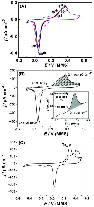 | ||
| Fig. 10 Cyclic voltammograms of Te UPD on Pd, (dE/dt = 50 mV s−1). (a) A selection of scans from the first 50 cycles of Te UPD. (b) 50th cycle of Te UPD (solid line) and Pd electrode response in 0.1 M HClO4 (dotted line). Inset: anodic part of the CV for irreversibly adsorbed Te after transfer of Pd electrode from 0.5 mM Te solution to fresh 0.1 M HClO4 solution. (c) Cyclic voltammogram for deposition and oxidation of bulk Te (solid line, TeB); anodic peak of 50th UPD scan, monolayer stripping (dotted line, TeM). | ||
In addition, it can be seen that Te deposition and oxidation are largely overlapped with adsorption/desorption of the O* and OH* at the Pd surface (Fig. 10b, dotted line). In this respect, the cathodic limit for the UPD was selected to ensure all the oxide on the surface of the Pd electrode is reduced (Fig. 10b).
It is interesting to note that with successive cycling the anodic stripping peak evolves from a single peak to a combination of two peaks. When the potential range was extended to initiate bulk Te deposition (Fig. 10c), the stripping peak for the bulk Te corresponds well with the first stripping peak observed for the Te mononlayer from the UPD of Te. This indicates that formation of near-bulk Te is also possible even in the UPD potential range. In this regard, bulk and monolayer stripping are used as colloquial terms to donate stripping of Te from a Te underlayer (bulk) and stripping of Te from a foreign Pd substrate (monolayer), respectively.
It was found that on the timescale of the CV measurements, the EQCM signal changed progressively from cycle to cycle, highlighting the complexity of the processes that occur simultaneously at the surface (OH* and O* adsorption/desorption, reduction of HTeO2+, oxidation of Te, redox transformations of the irreversibly adsorbed Te adatoms etc.). Consequently, slower EIS-EQCM experiments were absolutely essential to understand the Te UPD process on Pd.
Fig. 11 shows the EIS spectra of the electrode crystal during the UPD process. The model that best describes this response, shown in Fig. 11c, is also applicable to slow irreversible UPD processes,18 which do not contain any pathways for e.g. hypothetical perchlorate anion co-adsorption.
 | ||
| Fig. 11 Characterization of Te UPD on Pd using impedance spectroscopy: (a,b) extended Bode plots of the impedance spectra obtained in the cathodic scan; (c) a physical model of electrode/electrolyte interface in terms of equivalent electric circuit; (d) examples of the experimental data (open symbols) and the fitting results (solid lines) at some selected electrode potentials. | ||
Fig. 12 summarizes some of the results of the combined EIS-EQCM experiment. In the cathodic scan, a small decrease in the mass of the electrode can be observed (Fig. 12a). It is possible that this is mainly due to desorption of O* and OH* from the Pd surface. However, the onset of Te UPD can clearly be observed by the large increase in mass at potentials more negative than +0.1 V. Starting from this potential, the mass increase to the cathodic limit is around ∼450 ng cm−2 (Fig. 12a). When one considers that the mass of a 1:1 compact monolayer of Te on Pd would be ∼300 ng cm−2, it is clear that the measured mass change is equivalent to almost 1.5 monolayers of Te. Furthermore, the mass is found to increase further in the anodic scan until around +0.2 V, reaching a final difference of ∼600 ng cm−2, equivalent to two monolayers of Te deposited on the Pd(111)-like surface. We hypothesize that this additional deposition is triggered by the complete O* and OH* desorption (compare Fig. 10b and 12).
 | ||
| Fig. 12 Electrode mass change, the EQCM resonance resistance, C′dl(E) variations and the inverse of the charge transfer resistance variations during Te UPD on polycrystalline Pd (dE/dt = 0.3 mV s−1). | ||
Taking into account our EIS analysis and the dynamics of the mass change in the cyclic scan, we suggest that this additional mass increase is mainly due to Te deposition. Also, there is a pronounced mismatch between the start and final points of the Δm(E) curve (Fig. 12a), which can be explained by oxidation of the Pd surface and the irreversibly adsorbed Te.
The formation of Te bilayers on Au and Pt have been previously reported46,47 and imply that formation of a single monolayer of Te on an electrode substrate is extremely challenging in many cases. As the mass change is consistent with deposition of two monolayers of Te, and as no obvious evidence for ClO4− adsorption is found, we hypothesize that Te UPD leads to the formation of a bilayer on Pd.
The stability of the ΔR response on the cathodic and anodic scans suggests that, as with Cu and Pb on Pd, the effects of surface roughening and alloying are small (Fig. 12b). Further work, particularly using Pd single crystal surfaces, is however necessary for a more detailed characterization of the process. The irreversible nature of this UPD process is highlighted by the response of the double layer capacitance (Fig. 12c) and charge transfer resistance (Fig. 12d), which both display a ∼200 mV difference between the peak responses in the anodic and cathodic scans. These further supports the proposed model being appropriate to describe the Te UPD process on Pd.
Fig. 12e additionally shows the electrode mass change as a function of the charge (the data are acquired during the same scan). As can be seen from Fig. 12e, in the potential region of Te deposition, the Δm/Δq curve is not perfectly linear and considerably changes the slope, presumably due to concurrent Pd surface reduction and oxidation. However, the tentative slope (Fig. 12e) corresponds to the apparent molar weight for the adsorbate of approximately 160 g mol−1, assuming a four-electron process. This value is close to the molar weight of HTeO2+, which is present in the electrolyte solution. This fact additionally indicates the complex mechanism of Te adlayer deposition and oxidation, which requires further investigation to characterise in more detail.
To summarise, Te UPD on Pd is a comparatively complex process where Te is irreversibly adsorbed and forms a bilayer on the electrode surface. The potential regions of Te deposition/oxidation and Pd surface oxidation/reduction are overlapped. This process particularly highlights the value of the complementary combination of these techniques as the traditional methods of analysis would have been unable to allow a characterization of this extremely complex process.
3.5 Summary of UPD processes
Fig. 13 schematically summarizes the resultant surface layers for the UPD of Cu, Pb and Te on Pd, as well as summarizing the EEC's that illustrate the physico-chemical processes that occur during the formation of these overlayers. The UPD of Cu on Pd results in a compact Cu layer without co-adsorption of anions or significant surface alloying effects. The EEC for this process is the classical adsorption model, which illustrates that the Cu UPD process is, in general, electrochemically reversible; although the final stages appeared to be kinetically slow. The Warburg element was not found to contribute significantly within the selected frequency range. In the case of Pb UPD on Pd, this process occurs simultaneously with some H-UPD and H absorption. Due to the difference in the atomic radii of Pb and Pd it is not possible to form a compact layer in this situation, which leaves the facets where H-UPD can continue to take place. The irreversible adsorption of Pb is modeled in the EEC with a charge transfer resistance and Warburg impedance, while the concurrent H-UPD process is described by a parallel branch, which consists of a charge transfer resistance and adsorption capacitance. In contrast to the two above-mentioned UPD processes, the UPD of Te on Pd results in the formation of a compact bilayer on the electrode surface, which forms in the absence of perchlorate-containing anion co-adsorption or surface alloying. This slow electrochemically irreversible bilayer formation is described in the EEC simply by a charge transfer resistance.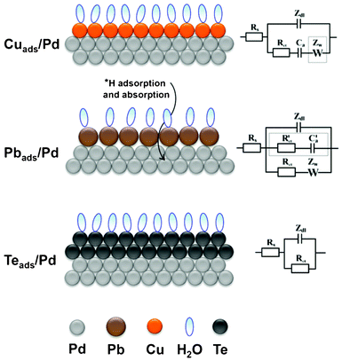 | ||
| Fig. 13 A schematic representation of Cu, Pb, and Te UPD on polycrystalline Pd and their corresponding equivalent electric circuit, respectively. | ||
4 Conclusions
Three representative systems, UPD of Cu, Pb and Te on Pd electrode, were characterized in situ by complementary combination of electrogravimetry and impedance spectroscopy techniques in one cyclic potential scan. Complementary analysis of the voltammetric and electrogravimetric data allowed an insight into the nature of the overlayer formed in the UPD processes. Assuming the polycrystalline Pd surface primarily consists of 111 facets; Cu UPD forms a monolayer with an apparent commensurate 1:1 coverage of Cu for each Pd atom on the Pd electrode. However, the final stages of the Cu UPD process were found to be kinetically slow, requiring slow potential scan rates to form a compact monolayer. Pb was found to form an uncommensurate atomic layer on the Pd electrode, with 1 Pb atom corresponding to 2 underlying Pd atoms. A more complex coverage was found for the Te UPD system on the Pd electrode, with the formation of a Te bilayer with a proportionate 1:1 correspondence with the Pd layer. This complexity arises in a potential range where the oxidized Pd surface is undergoing reduction; the completion of the oxide reduction appears to trigger the bilayer formation, although further study is necessary to fully understand the whole Te UPD process.
The combination of voltammetric studies and EIS-EQCM studies allow an efficient elucidation of the physical models of the electrode/electrolyte interface during the overlayer formation in terms of the equivalent circuits. It was found that the equivalent circuits, and hence UPD process, for each system varied. The Cu UPD process could be modelled with a classic model of reversible adsorption in the studied potential range. The Pb UPD process was modelled with a typical model of a slow irreversible adsorption, although an additional term was found to be necessary to describe the H-UPD and H absorption on the underlying Pd substrate. The Te UPD process could be modelled simply with only a charge transfer resistance. The study of the Te UPD process particularly shows the importance of combining in situ electrochemical methods to better understand the complex and dynamic systems.
The results demonstrate that the multidimensional data obtained by cyclic voltammetry; EQCM and EIS complement each other in elucidating different aspects of the interfacial dynamics. Such in situ multiparametric characterization of the electrode/electrolyte interface might provide an interesting way to deepen understanding of UPD processes, and thus, to guide the design of new systems for catalytic applications. The possible anion co-adsorption, competitive adsorption, or spontaneous surface alloying effects were investigated to evaluate the electrode/electrolyte interface status in these UPD processes. Such formed Cu, Pb and Te layers on Pd electrode showed no evidence of specific ClO4− anion co-adsorption and surface alloying effects, suggesting that the three systems studied in a perchlorate medium could be used as promising building blocks for catalytic applications, either as overlayers, or through the subsequent formation of near-surface alloys and surface alloys. Particularly, concerns should be provoked in the Cu UPD on Pd system with electrocatalytic activities for O2 reduction because a very clean Cu UPD layer is ensured, which is the prerequisite for the formation of a Cu/Pt(111) near surface alloy catalyst.16 It should be noted, however, that during the formation of Pb overlayers some evidence of the background H-UPD and H absorption to the underlying Pd substrate is observed. This will affect the application of such formed films to catalytic systems; however, subsequent catalytic reactions should preferentially be carried out at higher pH to negate the effect of H-UPD and absorption.
Acknowledgements
Financial support by the EU and the state NRW in the framework of the High Tech. NRW program is gratefully acknowledged. Alfred Ludwig and his co-worker (Chair of MEMS Materials, Institute of Materials, Faculty of Mechanical Engineering, Ruhr-Universität Bochum) are greatly thanked for clean-room access to deposit Pd on the EQCM-Chip.References
- M. Dincă, Y. Surendranath and D. G. Nocera, Proc. Natl. Acad. Sci. U. S. A., 2010, 107, 10337 CrossRef.
- M. W. Kanan and D. G. Nocera, Science, 2008, 321, 1072 CrossRef CAS.
- S. Mantha, V. A. Pedrosa, E.V. Olsen, V. A. Davis and A. L. Simonian, Langmuir, 2010, 26, 19114 CrossRef CAS.
- W. Jia, S. Schwamborn, C. Jin, W. Xia, M. Muhler, W. Schuhmann and L. Stoica, Phys. Chem. Chem. Phys., 2010, 12, 10088 RSC.
- B. A. Frontana-Uribe, R. D. Little, J. G. Ibanez, A. Palma and R. Vasquez-Medrano, Green Chem., 2010, 12, 2099 RSC.
- J.-M. Savéant, Chem. Rev., 2008, 108, 2348 CrossRef.
- J. Greeley, I. E. L. Stephens, A. S. Bondarenko, T. P. Johansson, H. A. Hansen, T. F. Jaramillo, J. Rossmeisl, I. Chorkendorff and J. K. Nørskov, Nat. Chem., 2009, 1, 552 CrossRef CAS.
- E. Herrero, L. J. Buller and H. D. Abruña, Chem. Rev., 2001, 101, 1897 CrossRef CAS.
- V. Rosca, M. Duca, M. T. de Groot and M. T. M. Koper, Chem. Rev., 2009, 109, 2209 CrossRef CAS.
- L. A. Kibler, A. M. El-Aziz, R. Hoyer and D. M. Kolb, Angew. Chem., Int. Ed., 2005, 44, 2080 CrossRef CAS.
- S. Uhm, S. T. Chung and J. Lee, Electrochem. Commun., 2007, 9, 2027 CrossRef CAS.
- Y. Xing, Y. Cai, M. B. Vukmirovic, W. P. Zhou, H. Karan, J. X. Wang and R. R. Adzic, J. Phys. Chem. Lett., 2010, 1, 3238 CrossRef CAS.
- F. Loglio, E. Castraioli, C. Bianchini, C. Fontanesi, M. Innocenti, A. Lavacchi, F. Vizza and M. L. Foresti, ChemSusChem, 2011, 4, 1112 CrossRef CAS.
- J. Greeley, T. F. Jaramillo, J. Bonde, I. Chorkendorff and J. K. Nørskov, Nat. Mater., 2006, 5, 909 CrossRef CAS.
- S. Hwang, J. Lee and J. Kwak, J. Electroanal. Chem., 2005, 579, 143 CrossRef CAS.
- I. E. L. Stephens, A. S. Bondarenko, F. J. Perez-Alonso, F. Calle-Vallejo, L. Bech, T. P. Johansson, A. K. Jepsen, R. Frydendal, B. P. Knudsen, J. Rossmeisl and I. Chorkendorff, J. Am. Chem. Soc., 2011, 133, 5485 CrossRef CAS.
- B.-Y. Chang, E. Ahn and S.-M. Park, J. Phys. Chem. C, 2008, 112, 16902 CAS.
- B. B. Berkes, A. Maljusch, W. Schuhmann and A. S. Bondarenko, J. Phys. Chem. C, 2011, 115, 9122 CAS.
- M. H. Huang, J. B. Henry, B. B. Berkes, A. Maljusch, W. Schuhmann and A. S. Bondarenko, Analyst, 2012, 137, 631 RSC.
- M. H. Huang, A. Maljusch, J. B. Henry, W. Schuhmann and A. S. Bondarenko, Electrochem. Commun., 2012, 20, 92 CrossRef CAS.
- G. Ritzoulis and N. Georgolios, J. Electroanal. Chem., 1994, 370, 219 CrossRef CAS.
- K.A. Soliman and L. A. Kibler, Electrochim. Acta, 2007, 52, 5654 CrossRef CAS.
- J. Okada, J. Inakai and K. Itaya, Phys. Chem. Chem. Phys., 2001, 3, 3297 RSC.
- A. Cuesta, D. M. Kibler and D. M. Kolb, J. Electroanal. Chem., 1999, 466, 165 CrossRef CAS.
- M. Shibata and S. Motoo, J. Electroanal. Chem., 1985, 194, 261 CrossRef CAS.
- L. Xiao, L. Zhuang, Y. Liu, J. Hu and H. D. Abruña, J. Am. Chem. Soc., 2009, 131, 602 CrossRef CAS.
- A. N. Correia, L. H. Mascaro, S. A. S. Machado and L. A. Avaca, Electrochim. Acta, 1997, 42, 493 CrossRef CAS.
- A. S. Bondarenko, G. A. Ragoisha, N. P. Osipovich and E. A. Streltsov, Electrochem. Commun., 2006, 8, 921 CrossRef CAS.
- G. A. Ragoisha, N. P. Osipovich, A. S. Bondarenko, J. Zhang, S. Kocha and A. Iiyama, J. Solid State Electrochem., 2010, 14, 531 CrossRef CAS.
- G. A. Ragoisha, A. S. Bondarenko, N. P. Osipovich and E. A. Streltsov, Electrochim. Acta, 2008, 53, 3879 CrossRef CAS.
- A. S. Bondarenko, I. E. L.Stephens, H. A. Hansen, F. J. Pèrez-Alonso, V. Tripkovic, T. P. Johansson, J. Rossmeisl, J. K. Nørskov and I. Chorkendorff, Langmuir, 2011, 27, 2058 CrossRef CAS.
- A. S. Bondarenko and G. A. Ragoisha, in Progress in Chemometrics Research, ed. A. L. Pomerantsev, Nova Science Publishers, New York, 2005, pp.89–102 (the program is available online at http://www.abc.chemistry.bsu.by/vi/analyser/) Search PubMed.
- A. S. Bondarenko, Anal. Chim. Acta, 2012, 743, 41 CrossRef CAS.
- R. Durand, J. Electroanal. Chem., 1979, 97, 293 CrossRef CAS.
- E. Sibert, R. Faure and R. Durand, J. Electroanal. Chem., 2002, 528, 39 CrossRef CAS.
- T. Pajkossy, J. Electroanal. Chem., 1994, 364, 111 CrossRef CAS.
- A. Lasia, in Modern Aspects of Electrochemistry, ed. B. E. Conway and R. E. White, Kluwer/Plenum, New York, 2002, vol. 35, p.1 Search PubMed.
- B. E. Conway, J. Barber and S. Morin, Electrochim. Acta, 1998, 44, 1109 CrossRef CAS.
- A. C. A. de Vooys, R. A. van Santen and J. A. R. van Veen, J. Mol. Catal. A: Chem., 2000, 154, 203 CrossRef CAS.
- J. Zhang, M. B. Vukmirovic, K. Susuki, F. Uribe and R. R. Adzic, J. Serb. Chem. Soc., 2005, 70, 513 CrossRef CAS.
- T. Chierchie and C. Mayer, Electrochim. Acta, 1988, 33, 341 CrossRef CAS.
- J. C. Love, D. B. Wolfe, R. Haasch, M. L. Chabinyc, K. E. Paul, G. M. Whitesides and R. G. Nuzzo, J. Am. Chem. Soc., 2003, 125, 2597 CrossRef CAS.
- M. Alvarez-Rizatti and K. Jüttner, J. Electroanal. Chem., 1983, 144, 351 CrossRef CAS.
- M. Grdeń, J. Kotowski and A. Czerwiński, J. Solid State Electrochem., 1999, 3, 348 CrossRef.
- I. Nicic, J. Liang, V. Cammarata, M. Alanyalioglu, U. Demir and C. Shannon, J. Phys. Chem. B, 2002, 106, 12247 CrossRef CAS.
- W. Zhu, J. Y. Yang, D. X. Zhou, S. Q. Bao, X. A. Fan and X. K. Duan, Electrochim. Acta, 2007, 52, 3660 CrossRef CAS.
- P. Rodriquez, E. Herrero, A. Aldaz and J. M. Feliu, Langmuir, 2006, 22, 10329 CrossRef.
Footnote |
| † M. H. Huang and J. B. Henry contributed equally to this paper. |
| This journal is © The Royal Society of Chemistry 2012 |