A nanogap–array platform for testing the optically modulated conduction of gold–octithiophene–gold junctions for molecular optoelectronics†
Ismael
Rattalino‡
ab,
Valentina
Cauda‡
*a,
Paolo
Motto‡
b,
Tania
Limongi
c,
Gobind
Das
c,
Luca
Razzari
c,
Francesca
Parenti
d,
Enzo
Di Fabrizio
c,
Adele
Mucci
d,
Luisa
Schenetti
d,
Gianluca
Piccinini
b and
Danilo
Demarchi
ab
aCenter for Space Human Robotics @PoliTo, Istituto Italiano di Tecnologia, C.so Trento, 21, 10129 Torino, Italy. E-mail: valentina.cauda@iit.it; Fax: +39 011 090 3401; Tel: +39 011 090 3436
bDepartment of Electronics, Politecnico di Torino, C.so Duca degli Abruzzi 24, 10129 Torino, Italy
cDepartment of Nanostructures, Istituto Italiano di Tecnologia, via Morego 30, 16163 Genova, Italy
dDepartment of Chemistry, University of Modena and Reggio Emilia, via G. Campi 183, 41125 Modena, Italy
First published on 5th October 2012
Abstract
We studied the light dependent conduction of gold–oligothiophene–gold molecular junctions as a fully–customized platform. The flexibility and novelty of the platform relies on its plug-and-play connection to an external electronic board to perform eight parallel nanogap fabrications by Electromigration Induced Break Junction (EIBJ) and molecular electrical characterization. In addition, the octithiophene molecules are synthesized ad-hoc to efficiently self-assembly and selectively bridge the nanogap electrodes upon deposition, which can be carried out directly and in parallel on the 8 nanogap array platforms. The high portability of the platform is well suited for in–situ microscopic and spectroscopic analyses. In particular, we tested the electrical functionality of the octithiophene molecular junctions by coupling electrical current–voltage (I–V) characterization with fluorescence and Raman spectroscopies. In addition, surface-enhanced Raman spectroscopy (SERS) was used for the first time to precisely correlate the position of the molecule with the conductance of the junction. Modulation of the electrical conductance can also be achieved by varying the light excitation wavelength. Such electrical transduction of the junction revealed a peak in molecule conduction around the light excitation wavelength of 450 nm, with a photoresponsive modulation of the current at low bias voltage up to 120% with respect to the initial value at 300 nm. The proposed ad-hoc platform design makes molecular junctions real working blocks, which can be interfaced with external circuitries to serve the function of electronic components or sensors and overcome the limitations of usability, cost and portability of traditional molecular contacting methods, such as Mechanically Controlled Break Junction (MCBJ) or scanning probe microscopy. We thus demonstrate that the optoelectronic properties of oligothiophenes can be exploited in the form of molecular junctions to fabricate optoelectronic devices for molecular electronics.
Introduction
The introduction of conductive organic molecules into electronic circuits has attracted increasing research interest with the aim of electrically characterizing the molecules and developing molecular electronic devices. As predicted by Aviram and Ratner in 1974,1 the use of single molecules as functional units in electronic circuits would show several advantages, including high efficiency, low cost, ability of self–assembling, peculiar optical and electronic properties. Moreover, by ad-hoc syntheses of the conductive molecular unit, one can self–tailor the geometry, composition and thus the electronic properties of this molecular circuit.Since the molecular dimension can reach up to 5 nm, thus below the traditional microfabrication resolution, several research efforts have been oriented to accommodate molecules inside nanogaps, which consist of a pair of metal electrodes separated by a nanoscopic space in between. Several methods have been reported to fabricate nanogap electrodes,2 such as electron and focused ion beam lithography, oblique angle shadow evaporation, controlled electrodeposition, electroplating and electromigration induced break junction (EIBJ). In particular EIBJ has been established as an effective technique for nanogap fabrication between 1 to 30 nm in width, due to its reliability, reproducibility and high throughput capability.3,4 These features make EIBJ fabrication a promising candidate in promoting molecular electronics on the industrial scale.
An effective and direct approach for introducing conductive molecules across nanogap electrodes is based on the self–assembly method, thus the selective bonding capabilities of organic molecules.5 The selectivity and consequent electrical conduction are obtained upon an accurate selection of their functional end–groups with respect to the metal electrodes, i.e. using thiol–, thioacetate– or thiophene–end functionalized oligomers. Self–assembled molecules on the two facing nanogap electrodes form the so–called Metal–Molecule–Metal junction (Me–M–Me),6 which is expected to become the fundamental building block of molecular electronic circuitries.
Conductive polymers, such as oligo–phenylene–ethynylene (OPE), oligo–phenylene–vinylene (OPV), polypyrroles, oligothiophene and polyaniline have been designated as among the most promising molecules for molecular electronics.7 Upon chemical modification, they offer the possibility of controlling the shape and electronic properties in a wide range of devices from insulators to superconductors. In particular, polythiophene and its derivatives have become one of the most attractive classes of conductive polymers, with numerous potential applications in the field of optoelectronics, including photodiodes, non–linear optical devices, phototransistors, solar cells, electroluminescent devices and chemical sensors.8–10 Oligothiophenes for optoelectronic applications have been widely studied in the form of self–assembled films.11 Conversely, few studies have been focused on the investigation of the photoresponsive properties of metal–oligothiophenes–metal molecular junctions. Yamada et al.12,13 studied the charge transport of single molecules of oligothiophenes by using Mechanically Controlled Break Junction (MCBJ) and Scanning Tunneling Microscopy (STM), Huang et al.14 focused on the photoresponsive properties of oligothiophene dithiol–bridged gold nanoparticles. Nevertheless, these approaches suffer from a lack of electric flexibility and a low yield to be exploited in molecular electronics, since the molecular junctions cannot be realistically interfaced to the macro–scale to serve an electronic or sensing function, without the limitations of handling one molecule at a time or requiring mechanical and bulky moving parts.
With these limitations in mind, this paper presents a nanogap–array platform designed by EIBJ parallel fabrication of up to 8 nanogaps and for testing the functionality of gold–oligothiophene–gold molecular junctions. The molecular platform can be easily interfaced at the macro–scale level with external circuitries and instruments to serve a function, either as an active component or as an integrated molecular sensor. Moreover the platform architecture provides parallelism and portability during all the experimental steps, consisting of the nanogap fabrication and the electrical, microscopic and spectroscopic characterizations of the molecular junctions. The used oligothiophene consists of 8 thiophene units with 4 octylsulfanyl chains in β position, which is an ad–hoc designed molecule to provide the anchor to nanogap electrodes, a proper electrical conduction and to impart solubility in organic solvents.
The customized preparation of the nanogap–array chip on an electronic circuit allowed us in-situ measurements, revealing the opto–modulated conductance behaviour of the octithiophene molecules, depending on the incident wavelength. The current–voltage (I–V) characteristic of the Me–M–Me junction was recorded under different illumination conditions, i.e. dark, white ambient light and at selected wavelengths in the range of 300–700 nm. Additionally, in–situ conductance, combined with fluorescence and surface-enhanced Raman spectroscopy (SERS) investigations, clearly showed the precise correspondence between the detected current and the molecule positioning into the nanogap–array.
These results demonstrate the possibility of introducing oligothiophenes in a nanogap array device, which can be easily interfaced at the macro–scale with circuitries and external equipment, in order to develop optoelectronic devices for molecular electronics.
Material and methods
Molecular design
The oligothiophene used [3′′′′,3′′′′′′,4′,4′′′–tetrakis(octylsulfanyl)–2,2′:5′,2′′:5′′,2′′′:5′′′,2′′′′:5′′′′,2′′′′′:5′′′′′,2′′′′′′:5′′′′′′,2′′′′′′′–octithiophene, Fig. 1] was obtained from 4–(octylsulfanyl)–2,2′'–bithiophene by one–pot oxidative coupling with FeCl3, and consisted of 8 thiophene units with 4 octylsulfanyl chains in the β position. The chemical synthesis of the molecule is described in detail in the work of Mucci et al.15 Such ad–hoc design, despite the head–to–head central junction, does not prevent planarization of the thiophene backbone and imparts solubility in organic solvents. The alkylsulfanyl chains surrounding the thiophene backbone work as insulating spacers between different molecules. These groups were used instead of thiols to prevent the polymerization between different molecules through the S–S bond formation. The thiophene ring and the alkylsulfanyl sulfur atoms can anchor the nanometric–sized gold gap, guaranteeing proper electron conduction.![The octithiophene used in this study [3′′′′,3′′′′′′,4′,4′′′–tetrakis(octylsulfanyl)–2,2′:5′,2′′:5′′,2′′′:5′′′,2′′′′:5′′′′,2′′′′′:5′′′′′,2′′′′′′:5′′′′′′,2′′′′′′–octithiophene]. Atoms in grey: carbon, in yellow: sulfur, in white: hydrogen.](/image/article/2012/RA/c2ra21484a/c2ra21484a-f1.gif) | ||
| Fig. 1 The octithiophene used in this study [3′′′′,3′′′′′′,4′,4′′′–tetrakis(octylsulfanyl)–2,2′:5′,2′′:5′′,2′′′:5′′′,2′′′′:5′′′′,2′′′′′:5′′′′′,2′′′′′′:5′′′′′′,2′′′′′′–octithiophene]. Atoms in grey: carbon, in yellow: sulfur, in white: hydrogen. | ||
Platform design and fabrication
The nanogap–array platform for molecule assembling and testing was prepared from 8 parallel gold wires on silicon wafer covered with 200 nm of silicon dioxide, by the EIBJ method. Fig. 2a shows the multi–level electronic board (NanoCube), which controls both the EIBJ nanogap fabrication and the electrical characterization of the molecular junctions. Fig. 2b shows a nanogap–array platform for molecule testing, which consists of a central silicon chip, bonded to a customized Printed Circuit Board (PCB). The dimension of the chip is 2.4 × 4.1 mm, the dimension of the platform is 10 × 20 mm. The chip, which is inserted in the NanoCube, is the core of the platform and was fabricated by standard optical lithography. The technological process is described in detail in the work of Demarchi et al.16 and in the Electronic Supplementary Information (ESI†). The chip layout is shown in Fig. 2c with 8 gold wires, which were about 25 nm thin, 6 μm long and 2 μm wide. Bonding wires attached onto the PCB and surrounding the chip were incorporated in a polydimethylsiloxane (PDMS) ring. The PDMS ring was used for protecting and insulating the bonding wires and confining the molecule deposition and washing solutions. The platform was designed to easily interface the molecular junctions with the macro-scale world in a plug–and–play method. Indeed, the PCB can be freely connected to and disconnected from any electronic apparatus, being an 8 parallel molecular junction array ready for in–situ measurements or as a building block for molecular electronics. Molecular junctions are independent but can be potentially connected to each other by the PCB to combine more complex electronics building blocks. The PCB is reusable and can be washed many times to remove the molecules so it can be used for different purposes and it is easily portable for performing Raman and Field Emission Scanning Electron Microscopy (FESEM) investigations.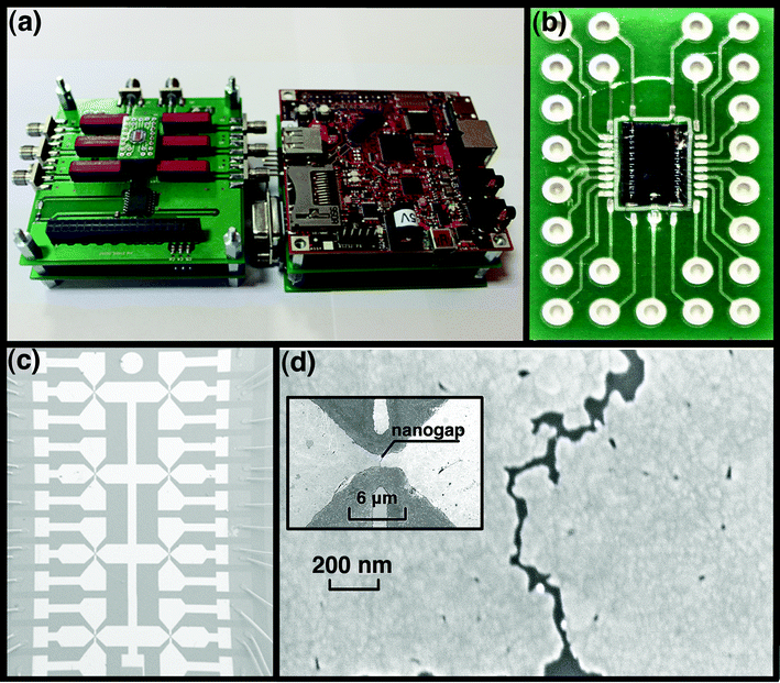 | ||
| Fig. 2 The fully customized molecular detection system on the nanogap–array testing platform. (a) The multi-level NanoCube, consisting of a driver board for input voltage waveform for electromigration (EIBJ), a measurement board and a switch board to allow the connection to external instrumentation. The chip on the PCB is hosted on the left side of the NanoCube; (b) The 8-nanogap–array chip wire–bonded to the customized PCB; (c) FE-SEM image showing the chip with the 8 butterfly-like nanogaps; (d) The electromigrated nanogap imaged by FE-SEM, the inset shows the gold wire at lower magnification. | ||
The EIBJ method used to fabricate nanogaps allows the reproducible fabrication of nanogaps, statistically 80% of them with the narrowest gap typically being lower than 10 nm in width17 (Fig. 2d). Once the PCB was connected to the Nanocube, the gold wires were electromigrated in parallel to obtain 8 nanogaps. A nanogap is shown around the center of the horizontal wire (inset of Fig. 2d), two gate electrodes for each nanogap were also provided, but not used in this work. For electromigration, the gold wires require an optimized geometry to facilitate and control the EIBJ process. In particular, a fine tuning of the wire cross–sectional dimension was performed:17,18 a small section of the wire is required to avoid an input current that is too high; however, if the section is too small, the thermal conductance decreases and the temperature of the wire tends to become excessive, leading to the gold melting.19 In order to provide the current density needed for the EIBJ process activation on the selected gold geometries, the NanoCube circuit was able to supply a current of at least 50 mA. The Measure Electronic Circuit, as a part of the NanoCube, was also able to measure the real time current flowing in the wire, to evaluate resistance variations from hundreds of mA (when the current is high and the break is not yet created) to some pA (for measuring the tunnel current upon the formation of the nanogap). The electromigration control algorithm is described in detail in the work of Motto et al.17 The electromigrated gold electrodes were characterized by Field Emission Scanning Electron Microscopy (FESEM, Auriga CrossBeam® Workstation, Carl Zeiss). In addition, we developed a wireless connection between the NanoCube and a host computer for sending the experimental data. This solution allowed also the use of the NanoCube in closed chambers where a wire interconnection can create difficulties, like the experiments under dark or fluorescent incident light. More details are provided in the ESI†.
Opto-electrical characterization
The electrical characterization of the sample took place during the electromigration procedure by means of the NanoCube board, as previously described. The octithiophenes were dissolved (100 nM) in tetrahydrofurane (THF, Chromanorm, >97%), which shows very low conductivity (1.5 × 10⁻⁸ S cm−1) and high volatility. The molecular solution was then deposited on the electromigrated nanogap–array chip, monitoring the conductance values until complete solvent evaporation. Additional washing steps in THF were also performed in order to remove the physically adsorbed molecules. The dried molecule–deposited nanogaps were then characterized for I–V curves from −1.5 to 1.5 V with the NanoCube under dark conditions and room temperature. I–V curves were also recorded under ambient light illumination and light irradiation from 300 to 700 nm using a Perkin Elmer LS55 fluorescence spectrometer equipped with a remote fiber optic accessory. The nanogap PCB was sealed into an aluminum dark box. The fiber optic projected the light from the hole at the top of the box, directly illuminating the samples. Fluorescence excitation (λem = 660 nm) and emission (λexc = 504 nm) spectra were recorded as well from the molecule–deposited nanogap electrode chips and from the molecules in THF solution at the same concentration (100 nM) for comparison.Raman analysis
Micro–probe Raman measurements were carried out by means of an inVia (Renishaw, New Mills, UK) microspectrometer, with a spectral resolution of 1.10 cm−1. The scattered Raman signal was dispersed with the help of a holographic grating of 1800 grooves mm−1. The samples were excited using the 633 nm laser wavelength in a backscattering configuration through a 100× objective (NA–0.90) and with an accumulation time of 2 s, keeping the laser power of 0.27 mW. The Raman band of the Si wafer at 520 cm−1 was used to calibrate the spectrometer. The scattering intensity of the oligothiophene molecule (concentration in the order of nM), deposited in the nanogap region, was collected in the range between 1045 and 2100 cm−1. Spectral data was analyzed using Renishaw WiRE software 3.0. The nanogap PCB was placed underneath a microscope objective (100×, long working distance). The in-situ electrical measurements (I–V curve) were performed in real–time during the Raman measurements.Results and discussion
I–V measurements in the array
Fig. 3a shows 8 current–voltage (I–V) and conductance–voltage (G–V) characteristics, which were measured across 8 molecular junctions of a chip array after the octithiophene deposition. Each characteristic describes the electrical conduction through octithiophene molecules bridging the two gold electrodes, forming one nanogap of the array.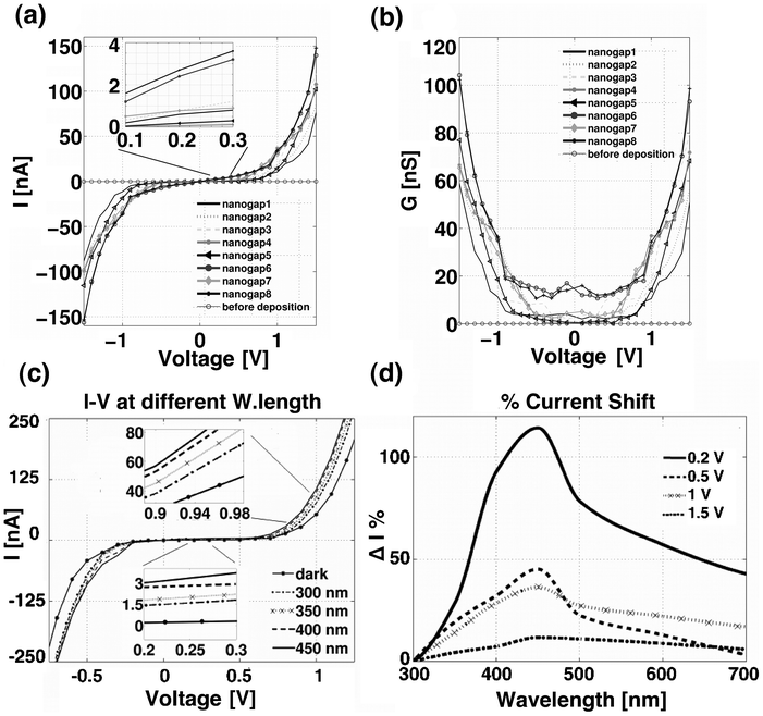 | ||
| Fig. 3 (a) 8 I–V characteristics of the Me–M–Me junctions, from the oligothiophene molecules deposited onto the 8 nanogap–array electrode chip; (b) 8 G–V characteristics obtained by deriving the I–V curves with respect to the applied voltage; (c) Effect of the incident light on the conduction in the Me–M–Me junction, I–V characteristics recorded at different excitation wavelengths of the incident light. The insets show a magnification of the I–V curve in the range 0.2–0.3 V and 0.9–0.98 V; (d) Percentage of current variation upon the light excitation wavelength used and as a function of the applied bias. | ||
All the I–V curves have the typical non–linear shape of a Me–M–Me junction.20–22 Below a certain threshold voltage, the current is low and weakly affected by the applied voltage, whereas it increases markedly with the applied voltage over the threshold. The region of the voltage comprised between the positive and negative thresholds is called the conductance gap, and can differ from 1 to 2 V in Fig. 3. G–V curves of Fig. 3b are obtained from I–V curves, by deriving the current with respect to the applied voltage. The G–V curve shape is a conductance well, where the width of the well coincides with the conductance gap.
For a qualitative explanation of this curve, we refer to the semiempirical formalism proposed by Datta et al.,21,22 which is the well known “toy model” of a molecular junction. In this model the width of the conductance gap is directly related to the energy difference between the Fermi level (Ef) of the junction at equilibrium and the closest molecular level (ε0), which could be either the highest occupied molecular orbital (HOMO) or the lowest unoccupied molecular orbital (LUMO).22 Once the voltage reaches the threshold value, the electrochemical potential of one of the electrodes is shifted from the Fermi level to the closest molecular level. At that point, the molecular orbital becomes a channel available for the transport of charge carriers, thus the current markedly increases. In the literature, the tunnelling effect is recognized as the main conduction mechanism up to a number of thiophene units around 11, whereas hopping contributions must be taken into account for longer molecules.12,13 Asymmetry of the curves with respect to 0 V can be observed for asymmetric molecular couplings to the contacts, in particular when one side of the molecule is strongly coupled to the electrode whereas the other side is weakly coupled.22 The asymmetry of the contacts induces an asymmetric distribution of the electric potential along the molecule, thus resulting in an asymmetric curve.
Each I–V curve can be considered as evidence of the presence of molecules inside the gap itself, bridging the two gold electrodes. Indeed the curve shape agrees with the theory of molecular conduction and the tunnel current before molecule deposition is around a few pA, which is a value three orders of magnitude lower than after deposition. We anticipate that the presence of the molecule is also confirmed by Raman and photocurrent spectroscopies, as discussed in the next sections.
In our system the estimation of a precise number of molecules involved in the conduction is difficult, since the accuracy in positioning the molecules, offered by proper tools like STM, MCBJ and Atomic Force Microscopy (AFM) is missing. In particular, these methods can continuously adjust the position of the electrodes to fit the molecule, until a single molecular bridge is formed across the electrode and the substrate,23 whereas the nanogap fixed structures cannot achieve high resolution in molecular detection.
The conductance of a single molecule of octithiophene was measured as around 50 nS at 100 mV by STM and MCBJ in the works of Yamada et al.12,13 This value did not seem consistent with the conductivities observed in our experiments, which were much lower than 20 nS at 100 mV (Fig. 3b), despite the presence of one or few molecules. This apparent inconsistency depends on both the strength of coupling between molecules and electrodes, which is affected by the contacting method, and by functional groups at the molecule extremities. In particular, MCBJ and STM methods can precisely accommodate the molecule among the electrodes obtaining stronger bonds, whereas horizontally fixed nanogaps, as those presented in this paper, typically show a lower conductance by several orders of magnitude. Salomon et al.24 reviewed several cases with different contacting methods. They noted that the difference in terms of current between the two systems with or without chemi–contacts could be up to 3 orders of magnitude for alkane thiol–based junctions. Hatanaka et al.25 used fixed nanogap electrodes fabricated by electrochemical plating and found values of conductivity around few pS at 100 mV for 24–mer–thiophenes, which is 1000 times lower than the value measured for 23–mer–thiophenes by Yamada et al.13 using MCBJ. In addition, Moth–Poulsen and Bjørnholm26 showed that the conductance can differ from pS up to μS for the same molecule, depending on the coupling strength induced by different terminal groups at the extremities. The weakest coupling was measured when the sulfur was embedded in the molecule chain close to the extremity, whereas the strongest coupling was obtained when the chain ended with a thiol–group. The octithiophene molecule used in this study is similar to the first case. Therefore, in our case the coupling is likely to be weak, with conductance around a few nS at low bias voltage.
However, both the number of molecules involved in conduction, and a strong coupling in molecular junctions are not essential factors for making possible molecular electronics. In this case, it is sufficient a characterization of each device in terms of the I–V curve and gating effect. The most important factor is the reproducibility of the physical support (nanogap), the possibility of working in parallel, of connecting devices and integrating new technologies with the old generation electronic devices. In addition, a weaker coupling could even be an advantage, compared to a strong one, in controlling the electron transfer, as the high broadening in strong couplings would reduce the dependence of the current on the gate voltage.26
Opto–electrical measurements
After the I–V characterization of the Me–M–Me junction on the 8–nanogap–array chip in dark conditions, we also investigated the effect of the incident light on the molecular conductance. Fig. 3c shows the absolute variation of the I–V curve, depending on different light wavelengths. Two insets expand the plot for low bias between 0.2 and 0.3 V and for high bias between 0.9 and 0.98 V. For low bias voltages inside the conductance gap, the current varies from a few tens of pA in dark conditions to a few nA under illumination, for higher bias voltages beyond the conductance gap, the current almost triples with respect to the dark condition. As expected, under light irradiation, the photon–generated excitons dissociated into either free electron–hole pairs or bound excitons,10,27 thus increasing the charge transport in the molecular junction. Some of the excitons possessed sufficient energy to jump over the tunnel barrier, thus resulting in a high current state of the Me–M–Me junction. All these effects were confirmed among different nanogaps and chips with a repeatable photo–electrical behaviour. The described light–controlled conductance effect was reported in the literature for other Me–M–Me junctions.28,29 This mechanism was interpreted as “low” and “high” current states, depending on the irradiation conditions and in the case of insufficient applied bias. Similarly in our experiments, the I–V characteristic becomes steeper as the applied bias increases above the conductance gap region. This behaviour was shown to be repeatable several times and totally reversible, and was also recorded by passing from dark to ambient white light. The I–V curve showed also a steeper behaviour as soon as an intense white light, produced by a common torch, was applied (see Fig. S–1 in the ESI†). The influence of the underlying silicon substrate on the conductivity enhancement has to be excluded due to the presence of 200 nm of silicon dioxide layer grown on it (see ESI† for further details on the chip fabrication process).Fig. 3d shows a photocurrent spectroscopy, where the photocurrent response of the molecular junction was measured as a function of the illumination wavelength at different applied voltages. The current values are calculated as a percentage of the initial value measured at an excitation wavelength of 300 nm. The peak of the current spectrum is located at around 450 nm; it is noteworthy that this wavelength is independent from the applied voltage. The relative increase in current is higher for lower bias, with a relative current peak value of around 120% at 0.2 V and of 10% at 1.5 V. At low bias, thus between the conductance gap at ±0.2 V, the incident light shows the predominant effect of increasing the charge transport through the generation of charge carriers, due to the excitation of the molecules. In contrast, at applied bias higher than the conductance gap (i.e. bias > 0.5 V), the contribution of the incident wavelength is still significant, as observed by the presence of the maximum peak of the current variation at 450 nm. However, this contribution is in competition with the applied voltage, producing a flattening of the relative electric current increase. The high applied bias leads indeed to an overall increase of the electric current across the Me–M–Me junction, resulting in a less marked increase of the relative current variation as a function of the wavelength variation, as observed in the Fig. 3d.
The photo-response of the molecular conduction was also investigated by the fluorescence spectra recorded directly on the octithiophene deposited on the nanogap–array chip and compared with the molecules in THF solution at the same concentration (100 nM, see the Experimental section for further details). The spectra recorded at an emission wavelength (λem) of 660 nm (Fig. 4a) shows an excitation peak at 482 nm for the octithiophene molecule in solution and at 507 nm when deposited on gold electrodes. Similarly, the emission peak recorded at λexc = 504 nm is located at 588 nm for the molecule in solution and at 648 nm for the Me–M–Me junction on the chip. These results clearly show the presence of a red-shift in both the excitation and emission spectra from the octithiophene in THF solution to the molecule when bound to the gold electrodes, throughout the whole chip.
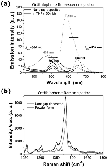 | ||
| Fig. 4 (a) Fluorescence excitation (solid lines, at λem = 660 nm) and emission spectra (dashed line, at λexc = 504 nm) of the 8–mer molecule in THF solution (100 nM, in grey) and deposited on the nanogap–array chip (in black). The excitation and emission spectra of three different chips were measured here. The arrows show the red–shift of both the excitation and emission peaks from the molecule in solution to the bound molecule in the Me–M–Me junction. (b) Micro–Raman spectra for the octithiophene molecule in powder form (grey curve, multiplied by 8) and deposited on the nanogap gold electrodes (black curve), showing an enhanced intensity due to the presence of the metallic electrodes. | ||
This shift could be attributed to the gold bridging by the oligomer in the solid state. Similarly the absorption and emission spectra of a thiophene–based polymer film evidence a red-shift with respect to the solution,30 indicating an increase of the conjugation length upon chain desolvation. This evidence was attributed to an appreciable degree of self–organization experienced by the polymer in the solid state. Some of us previously reported that the red-shift is due to the appearance of aggregate absorption shoulders.31 In particular these shoulders are identified as inter–chain excitons of octithiophene.
One should also note that the excitation and absorption peak intensities of the bound octithiophene are less intense than those of the molecule in THF solution. However, these intensities are not correlated to each other, since several effects on the molecule fluorescence at the solid state should be taken into account. First, fluorescence quenching of the octithiophene molecules could take place through transfer of the excitation energy to another molecule or to the gold metal surface. At small molecule–metal separations, the surface plasmon and electron–hole pair excitations in the metal can act as energy acceptors. The electron gas of the metal will dissipate this energy into the bulk through various scattering processes.32 In addition, fluorescence quenching can take place due to the packed conjugated oligomers interchain interaction,31,33 probably through π-stacking. It was also reported that films of polythiophenes obtained by casting or spin–coating featured a sharp drop of fluorescence quantum yield with respect to THF solutions, down to values of the order of 10−3.
Micro–Raman measurements were performed in the range of 1050–2100 cm−1 on the octithiophene molecules, deposited over the nanogap array chip and also in powder form, in order to verify their molecular Raman signature. SERS intensity of the molecule, bridging the electrodes, and micro–Raman intensity of the powder sample are plotted in Fig. 4b. Various characteristic peaks for the octithiophene, related to the C–S vibrations for aromatic group and δC–Hx vibrations, were observed at around 1072 cm−1 and 1158, 1211, 1354, 1442, 1481 cm−1, respectively.34 Raman spectra of both the powder and the molecules deposited in the region of the nanogap are very similar, showing no abrupt change in C–Hx and C–S vibrations, apart from a minor shift in Raman frequency. It is noteworthy that, though the concentration of the deposited oligothiophene molecules is in the order of nM, the Raman intensity is found remarkably enhanced due to the presence of metallic gold nanogap electrodes.
Furthermore, Raman area mapping measurements were carried out when a bias voltage was applied between the electrodes, in order to investigate the molecule presence in the region of the nanogap and the variation of Raman signal as a function of the applied voltage. An optical image of one of the measured nanogaps (sample 1) is shown in Fig. 5a. The grid area in the center of the image corresponds to the Raman mapping measurement area. 2D–analysis of baseline corrected SERS spectra, shown in Fig. 5b as a map of the recorded intensities, was performed for the reference band, centered at 1442 cm−1, related to the δC–Hx vibrations. A remarkable contrast in the analysis was observed, showing an increase in SERS signal close to the nanogap region. Since the molecules contain sulfur (due to the thiophene functional groups), the probability that this site attaches to gold is high. In addition, as clearly observed from the mapping analysis, the SERS intensity of the molecules residing close to the nanogap is high enough to consider the optical signal from the other part of the device as a background. Fig. 5c shows the merged image of both the SERS mapping image and optical image over a FESEM picture acquired on the same nanogap. The presence of the octithiophenes molecules nearby the nanogap electrodes, responsible for the conduction current due to the bridging the two electrodes, is clearly observed.
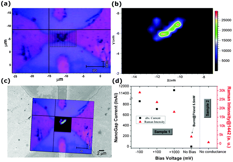 | ||
| Fig. 5 (a) Optical microscopy image of the nanogap area showing the Raman mapping grid; (b) 2–D analysis of baseline corrected SERS spectra, corresponding to the grid in (a) showing the intensity of the acquired signal from the octithiophene molecules; (c) Merged image of the Raman mapping and the FESEM image acquired on the same nanogap, (d) Electric current and acquired SERS intensities from the deposited octithiophenes as a function of the applied voltage. Sample 1: molecules bridging the gap (see (c)); sample 2: no current measured. | ||
Various SERS measurements were performed at the same time with in–situ electrical measurements and the outcomes of these tests are reported in Fig. 5d. An influence of the applied voltage over the SERS intensity is observed. SERS intensity for the reference band centered at 1442 cm−1 reached 29![[thin space (1/6-em)]](https://www.rsc.org/images/entities/char_2009.gif) 000 counts when the bias voltage was fixed to −100 mV (photocurrent: −860 nA), and decreased down to around 18000 counts for a bias of 1V (whereas higher photocurrent +11.6 μA was recorded). Interestingly, SERS intensity is found to be reducing further for nanogaps where no conduction is observed, due to the absence of molecular bridge over the electrodes (see, as an example, sample 2 in Fig. 5d). In order to verify the molecule damage effect over SERS intensity, we applied a high bias voltage (7 V) and 5.5 mW of laser for 1 min on the sample 1. The electrical current before and after was found to be invariable (10.9 μA at 1V as before and 0 A with no bias applied), but the expected damage on the molecules seems to affect the Raman measurement, causing a decrease in SERS intensity down to a value of 4000 counts (measurement labeled as “burnt” in Fig. 5d).
000 counts when the bias voltage was fixed to −100 mV (photocurrent: −860 nA), and decreased down to around 18000 counts for a bias of 1V (whereas higher photocurrent +11.6 μA was recorded). Interestingly, SERS intensity is found to be reducing further for nanogaps where no conduction is observed, due to the absence of molecular bridge over the electrodes (see, as an example, sample 2 in Fig. 5d). In order to verify the molecule damage effect over SERS intensity, we applied a high bias voltage (7 V) and 5.5 mW of laser for 1 min on the sample 1. The electrical current before and after was found to be invariable (10.9 μA at 1V as before and 0 A with no bias applied), but the expected damage on the molecules seems to affect the Raman measurement, causing a decrease in SERS intensity down to a value of 4000 counts (measurement labeled as “burnt” in Fig. 5d).
These findings prove not only a precise and unambiguous localization of the molecule between the conductive gap, but also highlight that the SERS intensities are strongly correlated to the applied voltage. We assume a direct relationship between the molecule characteristic vibrations and the electromagnetic field and power of the incident Raman laser.
Conclusions
This work demonstrates that the optoelectronic properties of oligothiophenes, which have been widely studied in the form of self–assembled films, can also be exploited in the form of molecular junctions to fabricate optoelectronic devices for molecular electronics. A modulation of the photocurrent in the wavelength range between 300–700 nm is possible up to a maximum value of around 120% for low bias voltage at a wavelength of 450 nm, with respect to the starting value at 300 nm.In order to provide usable building blocks for molecular electronics, we designed a fully customized testing platform, where molecular junctions are able to easily interface with external circuitries and equipment to serve their function. The platform satisfies important requirements in molecular electronics, which are parallelism in fabrication and characterization, portability with external equipment and low cost technology. The introduction of the molecules inside nanogaps was successfully performed by self–assembling, as proved by coupling electrical and SERS measurements, thus overcoming the limitations of portability and low yield of traditional molecular contacting methods, such as Mechanically Controlled Break Junction (MCBJ) or scanning probe microscopy.
Acknowledgements
We thank Guastella S., Chiodoni A., Aulika I. and Bejtka K. for assistance with the FESEM, Perrone D. and Dimonte A. for assistance with clean room processes, Trimarchi D. for assistance with the electronic board, Bestonzo M. for assistance with the PCB platform design.References
- A. Aviram and M. A. Ratner, Chem. Phys. Lett., 1974, 29, 277–283 CrossRef CAS.
- T. Li, W. Hu and D. Zhu, Adv. Mater., 2010, 22, 286–300 CrossRef CAS.
- Z. M. Wu, M. Steinacher, R. Huber and M. Calame, Appl. Phys. Lett., 2007, 91, 053118 CrossRef.
- D. E. Johnston, D. R. Strachan and A. T. C. Johnson, Nano Lett., 2007, 7(9), 2774–2777 CrossRef CAS.
- W. F. Smith, Nat. Nanotechnol., 2007, 2, 77–78 CrossRef CAS.
- H. B. Akkerman, P. W. M. Blom, D. M. De Leeuw and B. De Boer, Nature, 2006, 441, 69–71 CrossRef CAS.
- V. Saxena and B. D. Malhotra, Curr. Appl. Phys., 2003, 3, 293–305 CrossRef.
- S. Cheylan, A. Fraleoni–Morgera, J. Puigdollers, C. Voz, L. Setti, R. Alcubilla, G. Badenes, P. Costa–Bizzarri and M. Lanzi, Thin Solid Films, 2006, 497, 16–19 CrossRef CAS.
- L. Torsi, C. Malitesta, L. Sabbatini, P. G. Zambonin, A. Dodabalapur and H. E. Katz, Mater. Sci. Eng., C, 1998, 5, 233–236 CrossRef.
- F. Zhang, D. Wu, Y. Xu and X. Feng, J. Mater. Chem., 2011, 21, 17590–17600 RSC.
- I. F. Perepichka, D. F. Perepichka and H. Meng, Adv. Mater., 2005, 17, 2281–2305 CrossRef CAS.
- R. Yamada, H. Kumazawa, T. Noutoshi, S. Tanaka and H. Tada, Nano Lett., 2008, 8(4), 1237–1240 CrossRef CAS.
- R. Yamada, H. Kumazawa, S. Tanaka and H. Tada, Appl. Phys. Express, 2009, 2, 025002 CrossRef.
- W. Huang, G. Masuda, S. Maeda, H. Tanaka and T. Ogawa, Chem.–Eur. J., 2006, 12, 607–619 CrossRef.
- A. Mucci, F. Parenti, R. Cagnoli, R. Benassi, A. Passalacqua, L. Preti and L. Schenetti, Macromolecules, 2006, 39, 8293–8302 CrossRef CAS.
- D. Demarchi, P. Civera, G. Piccinini, M. Cocuzza and D. Perrone, Electrochim. Acta, 2009, 54(25), 6003–6009 CrossRef CAS.
- P. Motto, A. Dimonte, I. Rattalino, D. Demarchi, G. Piccinini and P. Civera, Nanoscale Res. Lett., 2012, 7, 113–120 CrossRef CAS.
- I. Rattalino, P. Motto, G. Piccinini and D. Demarchi, Phys. Lett. A, 2012, 376, 2134–2140 CrossRef CAS.
- M. L. Trouwborst, S. J. van der Molen and B. J. van Wees, J. Appl. Phys., 2006, 99, 114316 CrossRef.
- W. Hu, J. Jiang, H. Nakashima, Y. Luo, Y. Kashimura, K. Chen, Z. Shuai, K. Furukawa, W. Lu, Y. Liu, D. Zhu and D. K. Torimitsu, Phys. Rev. Lett., 2006, 96(2), 027801 CrossRef.
- S. Datta, Electronic Transport in Mesoscopic Systems, Cambridge University Press, Cambridge, U.K., 1995 Search PubMed.
- M. Paulsson, F. Zahid and S. S. Datta, Resistance of a Molecule. In Nanoscience, Engineering and Technology Handbook, ed. D. Brenner, S. Lyshevski and G. Iafrate, CRC Press, Boca Raton, Florida, U.S., 2002 Search PubMed.
- T. W. Kelley, E. Granstrom and C. D. Frisbie, Adv. Mater., 1999, 11(3), 261–264 CrossRef CAS.
- A. Salomon, D. Cahen, S. Lindsay, J. Tomfohr, V. B. Engelkes and C. D. Frisbie, Adv. Mater., 2003, 15(22), 1881–1890 CrossRef CAS.
- N. Hatanaka, M. Endo, S. Okumura, Y. Ie, R. Yamada, Y. Aso, K. Tanaka and H. Tada, Chem. Lett., 2007, 36(2), 224–225 CrossRef CAS.
- K. Moth–Poulsen and T. Bjørnholm, Nat. Nanotechnol., 2009, 4, 551–556 CrossRef.
- W. Hu, H. Nakashima, Z. Furukawa, Y. Kashimura, K. Ajito, Y. Liu, D. Zhu and K. Torimitsu, J. Am. Chem. Soc., 2005, 127, 2804–2805 CrossRef CAS.
- S. J. Van der Molen, J. Liao, T. Kudernac, J. S. Agustsson, L. Bernard, M. Calame, B. J. Van Wees, B. L. Feringa and C. Schönenberger, Nano Lett., 2009, 9(1), 76–80 CrossRef CAS.
- M. A. Mangold, M. Calame, M. Mayor and A. W. Holleitner, J. Am. Chem. Soc., 2011, 133(31), 12185–12191 CrossRef CAS.
- S. Cheylan, A. Fraleoni–Morgera, J. Puigdollers, C. Voz, L. Setti, R. Alcubilla, G. Badenes, P. Costa–Bizzarri and M. Lanzi, Thin Solid Films, 2006, 497, 16–19 CrossRef CAS.
- M. A. Lodi, M. Caselli, B. Zanfrognini, R. Cagnoli, A. Mucci, F. Parenti, L. Schenetti and G. Ponterini, Thin Solid Films, 2008, 516, 8731–8735 CrossRef.
- V. Cauda, A. Schlossbauer, J. Kecht, A. Zuerner and T. Bein, J. Am. Chem. Soc., 2009, 131, 11361–11370 CrossRef CAS.
- R. Cagnoli, A. Mucci, F. Parenti, L. Schenetti, M. Borsari, A. Lodi and G. Ponterini, Polymer, 2006, 47, 775–784 CrossRef CAS.
- G. Socrates, Infrared and Raman Characteristic Group Frequencies, John Wiley & Sons, Chichester, U.K., 2004 Search PubMed.
Footnotes |
| † Electronic Supplementary Information (ESI) available: See DOI: 10.1039/c2ra21484a |
| ‡ Authors contributed equally |
| This journal is © The Royal Society of Chemistry 2012 |