Synthesis of chemically bonded CNT–graphene heterostructure arrays†
Chandra Sekhar
Rout
a,
Anurag
Kumar
a,
Timothy S.
Fisher
*a,
Ujjal K.
Gautam
*bc,
Yoshio
Bando
c and
Dmitri
Golberg
c
aSchool of Mechanical Engineering, Purdue University, West Lafayette, Indiana 47907 and Birck Nanotechnology Center, Purdue University, West Lafayette, Indiana 47907, USA. E-mail: tsfisher@purdue.edu
bNew Chemistry Unit, Jawaharlal Nehru Centre for Advanced Scientific Research, Jakkur, Bangalore 560064, India. E-mail: ujjalgautam@jncasr.ac.in
cInternational Center for Materials Nanoarchitectonics, National Institute for Materials Science Namiki 1-1, Tsukuba, Ibaraki 305-0044, Japan
First published on 18th July 2012
Abstract
Carbon nanotube (CNT) and graphene constitute the two most exotic classes of functional carbon materials representing one-dimensional (1D) and two-dimensional (2D) nanostructures. With an intention of combining them together in to a single structure, in this communication, we report on vertically aligned, interconnected graphene arrays grown on arrays of CNTs.
Graphene, a monolayer of sp2 carbon, has emerged as an attractive two-dimensional (2D) nanomaterial with many interesting low-dimensional physical properties and potential applications.1–4 It is one of the strongest materials and possesses excellent electrical and thermal transport properties, suggesting potential miniaturization of electronic devices for diverse operating conditions.5–8 A carbon nanotube (CNT) is a rolled graphene sheet, amounting to further confinement of important properties from 2D to 1D.9 A heterostructure comprised of the integration of a 1D material having a basis in its 2D complement may deliver fascinating properties both for fundamental understanding as well as practical implications.5 Theoretical investigations of such structures reveal well defined deviations from the honeycomb carbon lattice near the junction.10 Recently, studies have also suggested the possibility of intriguing new transport properties, such as coupling and resonance of electronic states.11,12 It has been shown that stacked graphene carbon nanotubes can act as moderate photoconductors.13 In addition, efficient and economically viable hydrogen storage possibility has also been envisioned.14 Also, physical mixtures of CNTs and graphene exhibit high transparent conductance.15
Despite such promise, the fabrication of chemically integrated CNT–graphene heterostructures remains a challenge owing to the different conditions required for each structure. Graphene is usually generated by exfoliation of graphite or by controlled decomposition of hydrocarbons on a planar surface, while CNTs are obtained by a catalytic process with a hydrocarbon precursor.3,19–21 Kondo et al.22 have prepared a CNTs–graphene composite by chemical vapor deposition, where the graphene multilayers formed only at upper ends of CNTs array. Although aligned CNTs have been grown on a thin film of solution processed graphene, their microstructures are unknown.15 Herein due to the poor wettability of graphite surface by catalyst particles, aggregation and coalescence of the catalyst particles creates additional complications. Recently, graphene-like carbon nanowalls grown on CNTs have shown to act as electrodes in supercapacitors or other energy-conversion applications.16–18 It is to be noted that bottom-up synthesis of graphene on CNTs, with the potential of tailoring the growth and nature of each component individually has remained a challenge. In this communication, we describe a microwave plasma chemical vapor deposition (MPCVD) procedure enabling large-scale synthesis of CNT–graphene heterostructures throughout the CNTs array. We further establish that the two components are chemically bonded to each other with graphene outgrowths from the outer walls of the CNTs.
CNT–graphene heterostructures were synthesized in a three-stage procedure (Fig. S1, ESI†). In the first stage, aligned CNTs bundles were grown on a Si substrate coated with a trilayer (30 nm Ti/10 nm Al/3 nm Fe) catalyst. The MPCVD process gases were H2 with a flow rate of 50 standard cubic centimeters per minute (sccm) and CH4 (10 sccm), and the growth pressure and temperature were 10 Torr and 900 °C, respectively. The latter was controlled by an inductively heated graphite susceptor. A 200 W plasma was formed in the growth chamber, and CNT synthesis was carried out for 10 min. Deposition of graphene arrays on CNTs occurred in the second step simply by adjusting the above synthesis conditions in a continuous manner. The CNT array initially was exposed to 50 sccm H2 flow at a higher pressure of 30 Torr as well as higher plasma power of 700 W plasma with 900 °C substrate temperature for 10 min. In this intermediate step, the outer layers and the tips of the multiwalled CNTs become modified to create defect sites that act as nucleation centers for growing graphene layers. After 10 min, 10 sccm of CH4 was introduced into the chamber, and the reaction was carried out for 30 min under the same plasma power and pressure. We have previously demonstrated that, apart from Si, CNT arrays can be grown on other substrates such as Cu,23,24 and thus this synthesis of heterostructures provides a choice for substrate too.
A side-view SEM image of the CNT array is displayed in Fig. 1a. The length of the CNTs depends on the duration of growth. The height of the CNT layer is 30 μm in the present case, corresponding to an average growth rate of approximately 3 μm min−1. We estimate the number density of the CNT array to be approximately 1 × 10¹⁴ m−2. The inset in Fig. 1a is a top view of the CNT array showing a marked deviation from vertical alignment. This morphology is characteristic of MPCVD synthesis.25 Even though an overall perpendicular growth trend exists; CNTs bend in arbitrary directions locally (Fig. S2c, d, ESI†). The bent sections of the CNTs near the top may assist further to provide increased nucleation area for the growth and interconnection of graphene layers. The average diameter of CNTs is 50 nm. The walls of the CNTs are crystalline with closed ends (Fig. S2, ESI†).
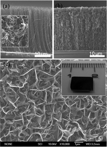 | ||
| Fig. 1 (a) A cross-section SEM image of an aligned CNT array and (b) CNT–graphene heterostructures grown on an Si substrate. A top view of the CNT array is shown in the inset of (a). (c) A top view SEM image showing the interconnected graphene layers grown on a CNT array. The inset in (c) is a photograph of the as-grown CNT–graphene heterostructures demonstrating large-scale synthesis. | ||
Cross-sectional and top views of the CNT arrays after growth of the graphene layers are presented in Fig. 1b and c and highlight two particular aspects. First, the layers nucleate and grow primarily along the top of the CNT layer. However, the plasma and the precursor CH4 gas can penetrate slightly into the CNT arrays, resulting in graphene layers being attached across the entire length of a CNT. Second, the layers at the top become interconnected forming a canopy of graphene petals (i.e., standing sheets of few layer graphene). The inset in Fig. 1c is a photograph of the as-grown product, indicating that the CNT–graphene heterostructures can be grown over large areas of greater than one square centimeter.
We further investigated the graphene petals and their contact with the CNT using high-resolution TEM. The petals typically display curling at their edges, which is similar to our previous studies of graphite petals grown on carbon fibers (Fig. 2a).26 Besides, these petals may be entirely amorphous or crystalline or may contain coexisting amorphous and crystalline regions (SAED studies). Fig. 2b shows an HRTEM image of a crystalline region of the petal seen in Fig. 2a. The corresponding fast Fourier Transform (FFT) pattern (inset of Fig. 2b) confirms the in-plane hexagonal symmetry. SEM images indicate a thickness of a few nm for the graphene petals. More precise estimation of the layer thickness by atomic force microscopy was difficult because removal of the intertwined nanostructures from the substrate leads to agglomeration. Fig. 2c and its inset show HRTEM images of the rolled up edge indicated by the dashed box in Fig. 2a. The layers are separated by 0.34 nm corresponding to the c-axis stacking of graphene. Fig. 2d contains the image intensity profile across the thickest portion of the rolled up edge, implying a maximum thickness of ∼5 nm for the graphene sheet. It should be noted that similar graphene sheets grown directly on planar substrates were found to have similar thickness.26
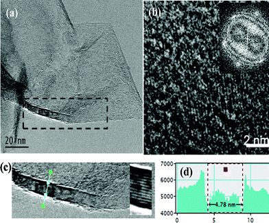 | ||
| Fig. 2 (a) TEM image of a graphene layer attached to a CNT. (b) HRTEM image of the layer. Inset shows a FFT pattern of the image, depicting the in-plane hexagonal symmetry. (c) High magnification image of the boxed region in (a) showing rolling up of the edge of the graphene layer. The inset in (c) shows 14 lattice fringes separated by a distance of 0.34 nm. (d) Intensity profile of the rolled up edge suggesting a maximum graphene sheet thickness of ∼5 nm near the edge. | ||
Fig. 3a shows an SEM image displaying a heterostructure wherein the CNT seamlessly merges onto the graphene sheet. We also observed graphene layers attached to several CNTs simultaneously, forming a network structure (Fig. S5, ESI†). A TEM image of a CNT–graphene heterostructure is shown in Fig. 3b in which a graphene sheet is in contact with the CNT at multiple places. In the high-resolution image at the region marked by an arrow (Fig. 3c), lattice fringes corresponding to both the CNT and the graphene layer are visible. The image further indicates that the graphene layers grow from the terminal atoms of the CNT layers. The encircled region in Fig. 3c shows the convergence of two thin graphene sheets. Likewise, different graphene layers possibly merge with each other epitaxially, forming the network structure seen in the top view SEM images in Fig. 1c.
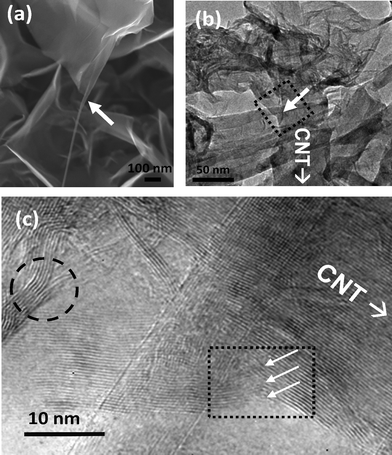 | ||
| Fig. 3 (a) SEM image showing a graphene sheet growing from a CNT (arrow shows tube-sheet transition point). (b) TEM image of CNT–graphene heterojunction (junction indicated by an arrow) (c) An HRTEM image near the junction indicated by a dotted rectangle in (b). Arrows depict the onset of growth of a few graphene layers from the walls of the CNT. The circled region shows a junction of two graphene layers inferring a probable attachment mechanism. | ||
We further characterized the CNT arrays before and after the growth of the graphene layers by using a confocal Raman microscope equipped with an excitation source of 532 nm under ambient conditions. The two samples (i.e., CNTs with and without the graphene petal canopy) were placed perpendicular to the probe micro-laser, so as to attribute the spectra primarily to the CNT (Fig. 4a) and the graphene layer (Fig. 4b). Both spectra contain three prominent peaks at 1340, 1590 and 2703 cm−1, which correspond to the D (disorder induced), G (tangential mode) and the 2D bands, respectively.27 However, the relative intensities of these peaks differ significantly in the two spectra. Table 1 highlights Raman features of CNT and graphene from this work and the literature.28–31 The intensity ratio of the D and G bands is a measure of z disorder, as expressed by the sp2/sp3 carbon ratio.32 With regards to the position of the D and G bands on the other hand, much depends on the local electronic structure of the material and hence was not considered in the present ensemble based study.33–35 For the CNT sample, the D peak is higher than the G peak with a ID/IG ratio of 1.43, owing to large deviations from the planar sp2 structure and formation of defects. The ID/IG ratio for the graphene sheets is 0.41, far lower than in CNTs, suggesting the characteristic planar structure of few-layer graphene. The lower ID/IG ratio suggests the presence of fewer numbers of edges normal to the surface as observed by other research groups.33–35 From our previous AFM measurements, the number of layers in the graphene sheets was estimated to be in the range of 5–10.26
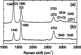 | ||
| Fig. 4 Raman spectra (acquired under ambient conditions with an excitation wavelength, λexc = 532 nm, acquisition area: ∼1 μm2) from (a) the unmodified CNT array and (b) the graphene layers grown on the top of the CNT array. | ||
In conclusion, we have demonstrated that the synthesis of heterostructures of carbon nanotubes with graphene is indeed realizable using microwave plasma chemical vapor deposition. The graphene layers were grown on top of an aligned CNT array on an Si substrate and are interconnected to form a network. Unlike previous reports where CNTs and graphene are physically mixed, our synthesis suggests an improved structure wherein the outer shells of a 1D carbon nanotube open up to form a 2D graphene layer. Additionally, this simple bottom-up technique is suitable for mass production on various substrates. However, the merging of the two nanostructures at the contact region is not perfectly seamless, thus suggesting that the synthesis requires further improvement.
Acknowledgements
UKG thanks the Department of Science and Technology (DST), India for financial support.References
- Y. Zhu, S. Murali, W. Cai, X. Li, J. W. Suk, J. R. Potts and R. S. Ruoff, Adv. Mater., 2010, 22, 3906 CrossRef CAS.
- A. K. Geim, Science, 2009, 324, 1530 CrossRef CAS.
- C. N. R. Rao, K. Biswas, K. S. Subrahmanyam and A. Govindaraj, J. Mater. Chem., 2009, 19, 2457 RSC.
- (a) X. H.uang, X. Qi, F. Boeya and H. Zhang, Chem. Soc. Rev., 2012, 41, 666 RSC; (b) H. Jiang, Small, 2011, 7, 2413 CAS.
- (a) H. Li, X. Cao, B. Li, X. Zhou, G. Lu, C. Liuman, Q. He, F. Boey, S. S. Venkatramana and H. Zhang, Chem. Commun., 2011, 47, 10070 RSC; (b) X. Dong, B. Li, A. Wei, X. Cao, M. B. Chan-Park, H. Zhang, L. J. Li, W. Huang and P. Chen, Carbon, 2011, 49, 2944 CrossRef CAS; (c) X. Cao, Q. He, W. Shi, B. Li, Z. Zheng, Y. Shi, Q. Yan and H. Zhang, Small, 2011, 7, 1199 CrossRef CAS.
- R. Grantab, V. B. Shenoy and R. S. Ruoff, Science, 2010, 330, 946 CrossRef CAS.
- X. Li, X. Wang, L. Zhang, S. Lee and H. Dai, Science, 2008, 319, 1229 CrossRef CAS.
- A. K. Geim and K. S. Novoselov, Nat. Mater., 2007, 6, 183 CrossRef CAS.
- Understanding Carbon Nanotubes; from basics to applications, ed. A. Loiseau, P. Launois-Bernede, P. Petit, S. Roche and J.-P. Salvetat, Springer, Berlin, 2006 Search PubMed.
- J. González, F. Guinea and J. Herrero, Phys. Rev. B: Condens. Matter Mater. Phys., 2009, 79, 165434 CrossRef.
- F. D. Novaes, R. Rurali and P. Ordejo, ACS Nano, 2010, 4, 7596 CrossRef CAS.
- V. Varshney, S. S. Patnaik, A. K. Roy, G. Froudakis and B. L. Farmer, ACS Nano, 2010, 4, 1153 CrossRef CAS.
- E. J. H. Lee, L. Zhi, M. Burghard, K. Mullen and K. Kern, Adv. Mater., 2010, 22, 1854 CrossRef CAS.
- G. K. Dimitrakakis, E. Tylianakis and G. E. Froudakis, Nano Lett., 2008, 8, 3166 CrossRef CAS.
- V. C. Tung, L.-M. Chen, M. J. Allen, J. K. Wassei, K. Neloson, R. B. Kaner and Y. Yang, Nano Lett., 2009, 9, 1949 CrossRef CAS.
- B. R. Stoner, A. S. Raut, B. Brown, C. B. Parker and J. T. Glass, Appl. Phys. Lett., 2011, 99, 183104 CrossRef.
- C. B. Parker, A. S. Raut, B. Brown, B. R. Stoner and J. T. Glass, J. Mater. Res., 2012, 27, 1046 CrossRef CAS.
- H.-C. Hsu, C.-H. Wang, S. K. Nataraj, H.-C. Huang, H.-Y. Du, S.-T. Chang, L.-C. Chen and K.-H. Chen, Diamond Relat. Mater., 2012, 25, 176 CrossRef CAS.
- M. S. Dresselhaus, G. Dresselhaus and P. Avouris, Carbon nanotubes: Synthesis, structure, properties and applications, Springer Verlag, Heidelberg, Germany, 2001, vol. 80 Search PubMed.
- C. N. R. Rao, A. K. Sood, K. S. Subrahmanyam and A. Govindaraj, Angew. Chem., Int. Ed., 2009, 48, 7752 CrossRef CAS.
- D. Rangappa, K. Sone, M. Wang, U. K. Gautam, D. Golberg, H. Itoh, M. Ichihara and I. Honma, Chem.–Eur. J., 2010, 16, 6488 CAS.
- D. Kondo, S. Sato and Y. Awano, Appl. Phys. Express, 2008, 1, 074003 CrossRef.
- B. A. Cola, X. Xu and T. S. Fisher, Appl. Phys. Lett., 2007, 90, 093513 CrossRef.
- B. A. Cola, J. Xu, C. R. Cheng, X. F. Xu, T. S. Fisher and H. P. Hu, J. Appl. Phys., 2007, 101, 054313 CrossRef.
- M. Meyyappan, L. Delzeit, A. Cassell and D. Hash, Plasma Sources Sci. Technol., 2003, 12, 205 CrossRef CAS.
- T. Bhuvana, A. Kumar, A. Sood, R. H. Gerzeski, J. Hu, V. C. Bhadram, C. Narayan and T. S. Fisher, ACS Appl. Mater. Interfaces, 2010, 2, 644 CAS.
- M. S. Dresselhaus, A. Jorio, M. Hofmann, G. Dresselhaus and R. Saito, Nano Lett., 2010, 10, 751 CrossRef CAS.
- E. F. Antunes, A. O. Lobo, E. J. Carat and V. J. Trava-Airoldi, Carbon, 2007, 45, 913 CrossRef CAS.
- W. Lin, K.-S. Moon, S. Zhang, Y. Ding, J. Shang, M. Chen and C. Wong, ACS Nano, 2010, 4, 1716 CrossRef CAS.
- D. Wei, Y. Liu, Y. Wang, Z. Zhang, L. Huang and G. Yu, Nano Lett., 2009, 9, 1572 CrossRef.
- Y. Hao, Y. Wang, L. Wang, Z. Ni, Z. Wang, R. Wang, C. K. Koo, Z. Shen and J. T. L. Thong, Small, 2010, 6, 195 CrossRef CAS.
- S. J. Chae, F. Gunes, K. K. Kim, E. S. Kim, G. H. Han, S. M. Kim, H.-J. Shin, S.-M. Yoon, J. Y. Choi, M. H. Park, C. W. Yang, D. Pribat and Y. H. Lee, Adv. Mater., 2009, 21, 2328 CrossRef CAS.
- N. Soin, S. S. Roy, C. OKane, J. A. D. McLaughlin, T. H. Lim and C. J. D. Hetherington, CrystEngComm, 2011, 13, 312 RSC.
- C. Jiang, J. Zhao, H. A. Therese, M. l. Friedrich and A. Mews, J. Phys. Chem. B, 2003, 107, 8742 CrossRef CAS.
- A. Malesevic, R. Vitchev, K. Schouteden, A. Volodin, L. Zhang, G. V. Tendeloo, A. Vanhulsel and C. V. Haesendonck, Nanotechnology, 2008, 19, 305604 CrossRef.
Footnote |
| † Electronic supplementary information (ESI) available. See DOI: 10.1039/c2ra21443a |
| This journal is © The Royal Society of Chemistry 2012 |