CdTe quantum dot sensitized hexaniobate nanoscrolls and their photoelectrochemical properties†
Feriha Eylul
Sarac
a,
Ceren
Yilmaz
b,
Funda Yagci
Acar
abc and
Ugur
Unal
*abc
aKoç University Chemistry Department, Rumelifeneri yolu, Sariyer, 34450, Istanbul, Turkey. E-mail: ugunal@ku.edu.tr; Fax: 90 212 338 1559
bKoc University, Graduate School of Science and Technology, Rumelifeneri yolu, Sariyer, 34450, Istanbul, Turkey. E-mail: ugunal@ku.edu.tr; Fax: 90 212 338 1559
cKoc University Surface Science and Technology Center, Rumelifeneri yolu, Sariyer, Istanbul, Turkey. Fax: 90 212 338 1559; E-mail: ugunal@ku.edu.tr; Tel: 90 212 338 1339
First published on 4th September 2012
Abstract
We have constructed hybrid quantum dot-layered niobate films with an electrophoretic deposition method. The structure and photoelectrochemical behaviour were demonstrated.
Synthesis of an effective semiconductor electrode is very important for solar energy conversion and photocatalytic applications.1,2 In these applications, semiconductors like TiO2 and ZnO are strongly favored and have been extensively studied.3–6 These wide band gap semiconductors are, however, not able to absorb the visible range of the solar spectrum and a sensitizer is required to absorb and transfer the energy of the visible range to a semiconductor. As utilization of sun light for energy production is getting more and more important, there have been many attempts to fabricate hybrid materials from semiconductor nanoparticles and nanostructures for the purpose of harvesting light in the visible region.
Layered oxides are also attractive and another important class of semiconductor materials in photocatalytic applications because a wide variety of compositions can be synthesized from their nanosheets. Their interlayer could be modified and nanosheets of layered oxides as building blocks can be hybridized with any organic or inorganic molecule for a specific purpose. K4Nb6O17 (KNbO) with a unique layered structure with two alternative interlayer spaces formed by repeating [Nb6O17]4− layers particularly proved itself as an alternative nanostructured semiconductor. Introduction of a wide range of cations and molecules into the interlayer of KNbO has been carried out on the basis of the ion-exchange principles and intercalation of large molecules, such as dyes or Ru(bpy)32+ complexes were accomplished.7,8 Another way to sensitize nanosheets of the layered materials is exfoliation-restacking sequence.9–11 These sensitized KNbO structures have been widely studied for their photocatalytic use for water splitting.8–10,12,13 Nanosheets of layered niobate combined with a sensitizer such as metal bipyridine complexes can effectively produce H2 and O2 in an aqueous medium under visible light.14
There are various methods to sensitize nanosheets of layered oxides. These are mainly based on the electrostatic attraction between negatively charged nanosheets and positively charged species like dye molecules, metal complexes and alkyl ammonium molecules.7–9,13,15,16 The interaction results in precipitates as a result of restacking between nanosheets and countercharged molecules. Then, the precipitates can be deposited on a substrate by pasting the precipitate and drying, electrophoretic deposition, etc.9,17 Another method in order to prepare thin films of nanosheets with various molecules/species is layer-by-layer method, which requires intensive care in controlling the deposition parameters and long preparation time.12,18,19 We have used electrophoretic deposition method in this study because the thickness of the film can be easily controlled by controlling the deposition parameters and the method results in strongly attached films on the substrate.
Quantum dots (QDs) have been investigated as an inorganic semiconductive sensitizer for wide band-gap semiconductors like TiO2 and ZnO and metal chalcogenide QDs have been preferred as a light harvesting semiconductor nanocrystal.20,21 The absorption range for these nano-sized materials can be tuned by adjusting their sizes and these short band-gap semiconductors can effectively harvest the visible range of the solar spectrum if strongly attached on the surface of a wide band gap semiconductor. In addition, they are good charge transfer agents and show good photostability.11,22–24
Although there are many reports on dye sensitized layered niobates, nothing is known about QD sensitized layered niobates and their applications. Here, we report the fabrication and photoelectrochemical properties of QD sensitized layered niobate films. Nanosheets of KNbO layered oxide was prepared according to the literature.9,25 Detailed information can be found in the ESI.† Cysteamine capped CdTe QDs (Cys-CdTe) are synthesized in an aqueous solution (see ESI†). In order to prepare CdTe/NbO hybrid material, 5 ml of Csy-CdTe QD solution was mixed with 5 ml of HNbO exfoliation solution under stirring. Immediate precipitation was observed. Following centrifuging and washing with acetonitrile three times, the precipitate was redispersed in 10 ml acetonitrile and sonicated in an ultrasonic water bath prior to the electrophoretic deposition. Dispersed Cys-CdTe/NbO hybrid in acetonitrile was deposited cathodically on an ITO electrode in a two-electrode cell. A platinum plate was used as a counter electrode. Details can be found in the ESI.†
XRD patterns of films showed broad (010) peaks instead of expected intense and sharp peaks for restacked layered oxides on the XRD pattern of films (see ESI†). This is a common feature for scrolled niobate structures.15 The broad peaks are an indication of the small number of nanosheet units stacked in the (010) direction. As discussed by Mallouk et al., niobate sheets scroll along low-index crystal directions.26 Asymmetry along the axis creates an intrinsic tension and nanosheets are rolled in order to relax the stress. Scrolled nanosheets can be easily seen by FESEM as shown in Fig. 1. Scrolls are several hundreds of nanometres long with a lateral thickness of 20–30 nm. Bright field images taken by a STEM detector on the FESEM also reveals the scrolled form of the nanosheets as seen in the figure.
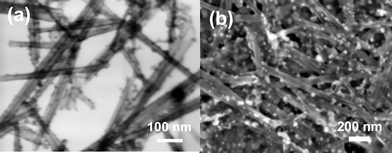 | ||
| Fig. 1 a) Bright field FE-SEM image of Cys-CdTe sensitized hexaniobate nanoscrolls taken with STEM detector on an FE-SEM b) FE-SEM image of CdTe/NbO film after electrophoretic deposition. | ||
It is very well known that the negatively charged layered oxide nanosheets restack and precipitate when mixed with cations and positively charged metal complexes. The precipitation is a result of electrostatic interaction between oppositely charged species,17 which resulted in an immediate precipitation after mixing Cys-CdTe QDs with niobate exfoliation solution. QDs can be seen clearly on niobate nanoscrolls as black dots in the bright field images of the niobate scrolls sensitized with Cys-CdTe QDs in Fig. 1a. EDX analysis of the bright spots in the FESEM image in Fig. 1b is a clear evidence of Cys-CdTe QDs on niobate nanoscrolls (see ESI†). The product is apparently not an intercalation compound but QDs were adsorbed on niobate nanoscrolls. Besides, density of QDs seems to be high and particles are larger than individual QDs. This implies that electrophoretic deposition carries high amount of QDs on the film.
X-Ray photoelectron spectroscopy (XPS) experiments also provided evidence for the presence of CdTe on NbO films (Fig. 2B). Te3d peak at ∼572 eV corresponds to 2+ state of Te.
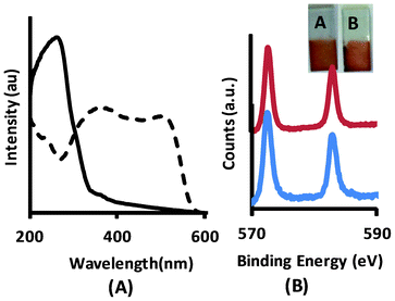 | ||
| Fig. 2 (A) UV-vis absorption spectrum of HNbO film (solid line) and Cys-CdTe/NbO film (dashed line), (B) Te3d XPS spectrum of CdTe/NbO film before (blue line) and after (red line) performing photocurrent experiments. The inset picture shows the photo of CdTe/NbO film A) before and B) after the photocurrent experiment. | ||
The diffuse reflectance UV-vis spectrum of the Cys-CdTe/NbO film is given in Fig. 2a in comparison with the niobate film only. As seen in the spectra, sensitization of NbO film with QDs shifts the absorption edge up to 600 nm in the visible region. The strong absorption in the visible region is compatible with the absorption spectrum of Cys-CdTe QDs (see ESI†). It is clear that the light harvesting ability of semiconductor niobate films in the visible light region was enhanced by the Cys-CdTe QDs.
It is evident from the results discussed above that CdTe QDs sensitized niobate nanoscrolls were successfully deposited on an ITO electrode. The photoelectrochemical properties of these films were investigated in order to reveal possible applications of such films in solar-energy conversion.
Photoelectrochemical experiments were carried out in a three electrode cell. Fig. 3 shows the i-t curve for Cys-CdTe/NbO films. Photocurrents were observed at bias voltage = 0 V vs. Ag/AgCl reference electrode under illumination with 250 Watt Xe light source (Newport). Electrolyte was a solution of 0.1 M Na2S + 0.1 M Na2SO3 + 0.1 methanol. I-t curves of films deposited from nanoscrolls without QDs and QDs without nanoscrolls were also taken under same conditions as a reference to elucidate the influence of QD sensitization. As can be seen in Fig. 3, Cys-CdTe/NbO film produces photocurrent under illumination of simulated sun light with AM1.5 filter (100 mW cm−2). The maximum current density for Cys-CdTe/NbO film was estimated around 40 μA cm−2. Photocurrent obtained from niobate films was around 2 μA cm−2 as seen in the figure. Photocurrent produced by QD film only was 8 μA cm−2 in the beginning but decreased over time (see ESI†). Photocurrent values reported for niobate nanosheets sensitized with dye molecules in the literature are below 10 μA cm−2 and our samples generated much higher photocurrent in the visible range than reported values.7,9,16,27,28 Photocurrent generated at different applied potentials showed that the film shows anodic photocurrent at band gap excitation (see Fig. 7 in ESI†). Zero photocurrent which could be attributable to current at flat-band potential was observed at −0.45 V vs. Ag/AgCl and the largest photocurrent was obtained around 0 V vs. Ag/AgCl.
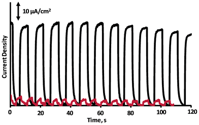 | ||
| Fig. 3 Photocurrent produced by CdTe/NbO (black solid line) and NbO without QD (red line) films in a solution of 0.1 M Na2S + 0.1 M Na2SO3 + 0.1 methanol. Experiments were performed by 250 Watt Hg-Xe Light source with 1.5 AM filter (100 mW cm−2). | ||
The observed photocurrent is in harmony with the UV-vis spectrum and as a result of electronic coupling between QDs and NbO nanoscrolls. The electron transfer from the conduction band of CdTe to the conduction band of the niobate is responsible for such behavior. The metal-to-metal charge transfer between two components can easily take place owing to the charge transfer capabilities. It is well known that the conduction band of the guest must be at higher potentials than that of host in order to have an efficient charge transfer. The schematic energy diagram of CdTe/niobate system vs. NHE is given in Fig. 4. The energy level of the conduction band of CdTe QD is at higher potentials than that of niobate nanosheets. This phenomenon brings about the efficient charge transfer from excited CdTe QDs to niobate nanosheets. Another evidence for the charge transfer is quenching in the photoluminescence of CdTe QDs. Photoluminescence of the CdTe was diminished after CdTe QDs were deposited together with the niobate nanosheets onto a substrate (see ESI†). Separation of photogenerated charge carriers is followed by the energy transfer from CdTe QDs to niobate nanosheets and hence reduces the electron-hole recombination. Electron-hole recombination is also prevented by the presence of hole scavengers, which are S2− and methanol in this study. S2− and methanol are known to be effective hole scavenger species for QDs and layered oxides, respectively.23,25
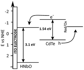 | ||
| Fig. 4 Energy band diagrams of CdTe QD and niobate nanosheets and possible energy transfer mechanism. | ||
We have carried out XPS analysis on the films after photocurrent experiments in order to examine the possible oxidation of CdTe QDs. No peak related to the Te4+ state on the Te3d spectrum was observed as seen in Fig. 2b. Since the QD retains the quantum dot oxidation state as revealed by the XPS spectrum we can conclude that the films are stable against oxidation during the photocurrent experiment. The inset pictures of the films in Fig. 2b before and after the photocurrent experiments are also evidence to support the stability of the film against photodegradation.
In conclusion, we have demonstrated the synthesis of hybrid films composed of CdTe QDs and layered hexaniobate nanoscrolls with electrophoretic deposition method. This method is easy and can be used for the synthesis of similar QD/layered oxide systems. Analysis of the hybrid films revealed that the CdTe/NbO films work as an efficient visible light harvester and quantum dot sensitized layered oxides could be an efficient system for solar applications like water splitting. Apparently, photocatalysts with high activity in the visible region can be designed easily using the provided method. Currently, we are investigating similar new hybrid materials for photochemical applications.
This work was financially supported by The Scientific and Technological Research Council of Turkey, project no: 109T759. The authors thank the Turkish Ministry of Development for the financial support provided for the establishment of Koc University Surface Science and Technology Center (KUYTAM).
References
- A. J. Bard, Science, 1980, 207, 139–144 CAS.
- D. A. Tryk, A. Fujishima and K. Honda, Electrochim. Acta, 2000, 45, 2363–2376 CrossRef CAS.
- B. Oregan and M. Gratzel, Nature, 1991, 353, 737–740 CrossRef CAS.
- M. Gratzel, J. Photochem. Photobiol., C, 2003, 4, 145–153 CrossRef CAS.
- Q. F. Zhang and G. Z. Cao, Nano Today, 2011, 6, 91–109 CrossRef CAS.
- D. Wei, Int. J. Mol. Sci., 2010, 11, 1103–1113 CrossRef CAS.
- Z. W. Tong, S. Takagi, H. Tachibana, K. Takagi and H. Inoue, J. Phys. Chem. B, 2005, 109, 21612–21617 CrossRef CAS.
- K. Maeda, M. Eguchi, S. H. A. Lee, W. J. Youngblood, H. Hata and T. E. Mallouk, J. Phys. Chem. C, 2009, 113, 7962–7969 CAS.
- U. Unal, Y. Matsumoto, N. Tamoto, M. Koinuma, M. Machida and K. Izawa, J. Solid State Chem., 2006, 179, 33–40 CrossRef CAS.
- E. M. Sabi, R. L. Chamousis, N. D. Browning and F. E. Osterloh, J. Phys. Chem. C, 2012, 116, 3161–3170 Search PubMed.
- I. n. Mora-Seró, S. Giménez, F. Fabregat-Santiago, R. Gómez, Q. Shen, T. Toyoda and J. Bisquert, Acc. Chem. Res., 2009, 42, 1848–1857 CrossRef.
- W. J. Youngblood, S. H. A. Lee, K. Maeda and T. E. Mallouk, Acc. Chem. Res., 2009, 42, 1966–1973 CrossRef CAS.
- K. Maeda, M. Eguchi, W. J. Youngblood and T. E. Mallouk, Chem. Mater., 2008, 20, 6770–6778 CrossRef CAS.
- Y. Ebina, N. Sakai and T. Sasaki, J. Phys. Chem. B, 2005, 109, 17212–17216 CrossRef CAS.
- M. A. Bizeto, W. A. Alves, C. A. S. Barbosa, A. M. D. C. Ferreira and V. R. L. Constantino, Inorg. Chem., 2006, 45, 6214–6221 CrossRef CAS.
- K. Yao, S. Nishimura, Y. Imai, H. Wang, T. L. Ma, E. Abe, H. Tateyama and A. Yamagishi, Langmuir, 2003, 19, 321–325 CrossRef CAS.
- U. Unal, Y. Matsumoto, N. Tanaka, Y. Kimura and N. Tamoto, J. Phys. Chem. B, 2003, 107, 12680–12689 CrossRef CAS.
- M. Fang, C. H. Kim, G. B. Saupe, H.-N. Kim, C. C. Waraksa, T. Miwa, A. Fujishima and T. E. Mallouk, Chem. Mater., 1999, 11, 1526–1532 CrossRef CAS.
- L. Li, R. Ma, Y. Ebina, K. Fukuda, K. Takada and T. Sasaki, J. Am. Chem. Soc., 2007, 129, 8000–8007 CrossRef CAS.
- P. V. Kamat, J. Phys. Chem. C, 2008, 112, 18737–18753 CAS.
- S. Rühle, M. Shalom and A. Zaban, ChemPhysChem, 2010, 11, 2290–2304 CrossRef.
- J. H. Bang and P. V. Kamat, ACS Nano, 2009, 3, 1467–1476 CrossRef CAS.
- V. Chakrapani, D. Baker and P. V. Kamat, J. Am. Chem. Soc., 2011, 133, 9607–9615 CrossRef CAS.
- P. V. Kamat, Acc. Chem. Res., 2012 Search PubMed.
- K. Izawa, T. Yamada, U. Unal, S. Ida, O. Altuntasoglu, M. Koinuma and Y. Matsumoto, J. Phys. Chem. B, 2006, 110, 4645–4650 CrossRef CAS.
- G. B. Saupe, C. C. Waraksa, H. N. Kim, Y. J. Han, D. M. Kaschak, D. M. Skinner and T. E. Mallouk, Chem. Mater., 2000, 12, 1556–1562 CrossRef CAS.
- K. Yao, S. Nishimura, T. L. Ma, K. Okamoto, K. Inoue, E. Abe, H. Tateyama and A. Yamagishi, J. Electroanal. Chem., 2001, 510, 144–148 CrossRef CAS.
- X. T. Pian, B. Z. Lin, Y. L. Chen, J. D. Kuang, K. Z. Zhang and L. M. Fu, J. Phys. Chem. C, 2011, 115, 6531–6539 CAS.
Footnote |
| † Electronic Supplementary Information (ESI) available: Experimental details and XRD, EDX and UV-vis spectra of the CdTe/NbO films. See DOI: 10.1039/c2ra21252h |
| This journal is © The Royal Society of Chemistry 2012 |