Super-long barnesite Na2V6O16·3H2O nanobelts for aligned film electrodes with enhanced anisotropic electrical transport
Yan
Xue
a,
Jian
Wu
a,
Hanyang
Zhang
a,
Yi
Luo
a,
Xiaodong
Zhang
a,
Zuliang
Du
b and
Yi
Xie
*a
aHefei National Laboratory for Physical Sciences at Microscale, University of Science & Technology of China, Hefei, 230026, P.R. China. E-mail: yxie@ustc.edu.cn; Fax: 86 551 3606266; Tel: 86 551 3603987
bKey Lab for Special Functional Materials of Ministry of Education, Henan University, Kaifeng, 475001, P. R. China
First published on 13th June 2012
Abstract
Developing a novel, aligned super-long nanobelt film electrode is essential for achieving outstanding electrical transport properties. However, pursuing a convenient way to fabricate an aligned super-long nanobelt film electrode has been a challenge so far. Herein, the aligned super-long barnesite Na2V6O16·3H2O nanobelt film electrode is realized as a dense and thick film for the first time by a convenient solution route, providing a new strategy to synthesize aligned nanobelt film electrodes. The Na2V6O16·3H2O nanobelts with lengths of 100–200 μm growing along [010] are fabricated successfully, and the super-long single nanobelt enables the first investigation of electrical transport property. Encouragingly, the individual nanobelt with aspect ratios exceeding 1000 has a high conductivity of ∼100 S m−1. Furthermore, the synthetic aligned super-long barnesite Na2V6O16·3H2O nanobelt film electrode displays an enhanced anisotropic electrical transport property and good electrical conductivity, presenting an ideal candidate as a nanoelectrode.
1. Introduction
For over a century we have been able to directly convert chemical energy into electrical power.1 But the electrode is responsible for the good performance of the battery. In response to emerging ecological concerns, nanoelectrodes have been an important breakthrough to meet increasing energy demands. Nanoelectrodes are defined as electrodes with a critical dimension in the nanometer range, where the “critical dimension” refers to the defining dimension that controls the electrical response. Generally, nanoelectrodes are distinguished by the length scale and critical dimension of interest being in the range from one nanometer to hundreds of nanometers. Beyond the dimensionality, of greater scientific and technological interest are the unique properties that have been reported when materials and devices are fabricated in the nanometer scale. In the electrical studies and applications, their great advantages including short path lengths for electrical transport, higher electrode/electrolyte contact areas and so on.2 Metallic nanowires, carbon nanotubes, magnetic nanoparticles, metal oxides, nanowires and nanotubes have all been employed to fabricate nanoelectrodes. However, one dimensional nanostructures such as nanowires and nanobelts, represent the smallest dimension for the efficient transport of electrons and excitons and thus are ideal building blocks for the hierarchical assembly of functional nanoscale electronic structures. Therefore, as one of the most important types of one dimensional (1D) nanostructures, nanobelts have been demonstrated as the favorable fundamental building blocks for nanoelectrodes.3 Because nanobelts with a rectangular cross-section and well-defined faceted surfaces enable the observation of unique piezoelectricity,4,5 and efficient 1D electrical transport, which are determined by their anisotropic shape.6 Confessedly, with the decreasing nanoscale, the electrical conductivity of the nanoparticle is reduced because of a drastic increase in the density of grain boundaries. To achieve the substantial potential of nanobelts in nanoelectrodes will require the controlled assembly of nanobelts into aligned nanobelt thin films to yield a novel electrode. In brief, a typical example of a parallel assembly of nanobelts shows that virtually all the nanobelts are aligned along one direction. This aligned nanobelt film electrode has high carrier mobility due to its conducting channels formed by multiple parallel single-crystal nanobelt paths.7 Notably, the anisotropic shape of the nanobelts and contact resistance between inter-nanobelts would inevitably lead to anisotropic electrical transport. (Scheme 1).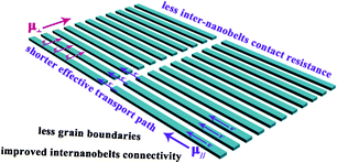 | ||
| Scheme 1 A schematic representation of the expected advantages of the aligned nanobelt film electrode. | ||
Recently, considerable progress has been developed to prepare ordered nanobelt structures over micrometer length scales via various strategies such as microfluidic8 and electric field-assisted assembly approaches.9 Although electric fields enable good control over assembly, this method is also limited by electrostatic interference between nearby electrodes as separations are scaled below the micrometer level and the requirement of extensive lithography to fabricate the electrodes for assembly of multiple nanoelectrodes. The microfluidic method needs complicated steps and elaborate manipulation. In summary, these methods are too complicated to fabricate dense and thick films as aligned nanobelt film electrodes in high yields over large areas without high prices or dangerously high voltages. In addition, the conventional method of fabricating a film electrode by grinding nanobelts into fine powders would inevitably destroy the conducting channel of electrical transport, leading to increased inter-nanobelt contact resistance ascribed to more grain boundaries. In other words, the conventional way to fabricate a film electrode would decrease the electronic conductivity of the film electrodes.10 As a result, developing a facile, safe, economic, and convenient way to fabricate the aligned nanobelt film electrode with good conductivity has still been a great challenge so far.
As is well known, vanadium oxides and their derived compounds have attracted much attention due to their outstanding structural flexibility and unique chemical and physical properties.11 These special properties allow them potential applications in many areas, such as catalysts and 12 electrical and optical devices,13,14 especially nanoelectrodes for energy storage and saving applications.15 As one of the most important vanadium oxide compounds, barnesite Na2V6O16·3H2O has been studied as a typical electrode material applied in lithium ion batteries, and its layered structure is favors the insertion/desertion of lithium ions.16 Very recently, we found that Na2V6O16·3H2O is a novel semiconductor with a band gap of 1.9 eV, both theoretically and experimentally.17 In recent years, although many ways have been developed to synthesize Na2V6O16·3H2O in complicated solutions, the various oxidants might bring about an increase of impurities in the final product. Thus, it is necessary to develop more facile, mild and easily controlled methods to synthesize Na2V6O16·3H2O nanobelts. In this study, to avoid the use of oxidants, a precursor route where the compounds were in the correct valence was put forward to simplify the synthesis steps. Na3VO4 supplied the correct valence of vanadium and has been successfully applied to fabricate super-long Na2V6O16·3H2O nanobelts in high yield. This approach for synthesis of super-long Na2V6O16·3H2O nanobelts is proven to be efficient, economical, and easy to scale up in industrial production in the absence of the oxidants and vacuum condition. The synthetic super-long single crystalline nanobelts enable the possibility of further research on the electrical transport of a single nanobelt. Due to its electrical transport channel without barriers and grain boundaries in the single crystalline Na2V6O16·3H2O nanobelt, it displays excellent electrical transport properties, indicating its potential application for nanoelectrodes. In fact, the synthetic super-long nanobelts also allows the feasible investigation into an aligned nanobelt film electrode. More importantly, sheet resistances of the aligned nanobelt thin films that had current flowing perpendicular to the nanobelt alignment direction were compared to those that had current flowing parallel to the nanobelt alignment direction. We highlighted that perpendicular devices showed ∼10 fold greater sheet resistance than parallel devices. We highlight the enhanced anisotropic electrical transport shown by the aligned Na2V6O16·3H2O nanobelt film electrode which are an ideal candidate for nanoelectrodes.
2. Experimental section
Synthesis of capsule-like aligned Na2V6O16·3H2O nanobelt films
Barnesite Na2V6O16·3H2O nanobelts were synthesized by a facile hydrothermal process. In a typical process, 2 mmol Na3VO4 (0.800 g) was dissolved into 30 mL distilled water and stirred strongly for 10 min. After adjusting the pH to about 3.0–6.0 with 2 M HCl, the whole solution was orange. Then, the solution was transferred to a Teflon-lined stainless steel autoclave with a capacity of 42 mL, and the autoclave was sealed and maintained at 200 °C for 24 h. The reaction system was then allowed to cool to room temperature. Once the reaction was over, the capsule-like sample was taken out and washed with deionized water and pure ethanol respectively to remove any possible ionic remnants, then dried in a vacuum oven at 50 °C for 5 h. For comparison, the unaligned nanobelt film was obtained by dispersing the aligned nanobelt film in deionized water using the sonication method. Then, to obtain the unaligned nanobelt film, the whole solution was filtrated by vacuum.Characterization methods
X-ray powder diffraction was performed using a Philips X'Pert Pro super diffractometer with Cu-Kα radiation (λ = 1.54178 Å). The SEM images were taken with a Field Emission Scanning Electron Microscope (JEOL JSM-6700F). The transmission electron microscopy images (TEM), high resolution transmission electron microscopy images (HRTEM) and selected area electron diffraction patterns (SAED) were gathered on JEOL-2010 transmission electron microscopes at an acceleration voltage of 200 kV. X-ray photoelectron spectroscopy measurement was performed on a VGESCALAB MKII X-ray photoelectron spectrometer with an excitation of Mg-Kα = 253.6 eV.Electrical transport property of a single Na2V6O16·3H2O nanobelt
In order to measure the electrical transport properties of the single Na2V6O16·3H2O nanobelt, the synthetic nanobelts were first dispersed in ethanol using the sonication method, and then these nanobelts were assembled on a pair of Pt electrodes by dielectrophoresis. For dielectrophoresis, an ac voltage with 10 Vp.p (peak to peak) and 50 kHz was applied to the Pt electrode pair. The inset of Fig. 4 shows the SEM image of a single Na2V6O16·3H2O nanobelt assembled on a pair of Pt electrodes. The spacing intervals between the two Pt electrodes is 4 μm.20Electrical measurement of the Na2V6O16·3H2O nanobelt film electrodes
Prior to actual testing, a totally dried Na2V6O16·3H2O nanobelt film was first cut into a rounded film with a diameter of 1 cm. Two point measurements are used to measure the sheet resistance of the nanobelt film electrodes. Copper electrodes were deposited on the aligned nanobelt films by pasting Ag slurry. The current–voltage (I–V) characteristics of the device were recorded at Electrochemical Workstation at room temperature. The inset of Fig. 6d shows the digital photographs of Na2V6O16·3H2O nanobelt films with copper electrodes.3. Results and discussion
Herein, with the presence of HCl as the acidity regulator, we have successfully fabricated novel barnesite Na2V6O16·3H2O nanobelts growing along [010] with the super-long length of 100–200 μm in a high yield of 99% for the first time. The related XRD pattern of the grounded sample is shown in Fig. 1a, all of the reflection peaks can be readily indexed to monoclinic Na2V6O16·3H2O with a space group of P2/m (JCPDS card No.16-0601, a = 12.17 Å, b = 3.60 Å, c = 7.78 Å, and β = 95.03°), no other phases can be detected. Moreover, the XPS survey spectrum shown in the Fig. 1(b) revealed that the as-obtained product consists of the elements Na, V and O, while no evident impurities were detected. The high-resolution XPS for the Na 1s region (Fig. 1c) showed the core level at 1071.2 eV with the dominant Na signal assigned to Na+. The high-resolution XPS for the V 2p region (Fig. 1d) showed the core level at 517.3 eV with the dominant V signal assigned to V5+. All these results indicated that the as-obtained product is monoclinic Na2V6O16·3H2O, and the XPS spectra showed no evident impurities detected in the samples (resolution limit: 1 at.%), in accordance with the previous reports.18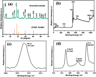 | ||
| Fig. 1 (a) Grounded sample and standard (bottom) XRD patterns of the Na2V6O16·3H2O product. (b) XPS survey spectrum. (c) XPS spectra of Na 1s peak. (d) XPS spectra of O 1s peak and V 2p peak. | ||
Super-long barnesite Na2V6O16·3H2O nanobelts on a large scale are depicted in SEM images, as shown in Fig. 2a and b, displaying that a 100% morphological yield of nanobelts with a uniform size distribution has been achieved in this work. These nanobelts have a typical length of up to 100 μm, a width of about 100–200 nm, and a thickness of about ca. 40 nm, consistent with the obtained nanobelts shown in the TEM images of Fig. 2c. Moreover, the high-resolution TEM (HRTEM) images and selected area electron diffraction (SAED) patterns shown in Fig. 2d also provide microscopic structural information for Na2V6O16·3H2O. An individual Na2V6O16·3H2O nanobelt is single crystalline, as revealed by the diffraction pattern of the bright spot SAED pattern and the associated HRTEM with the electron beam perpendicular to the surface of the nanobelt. The interplanar distances of 0.34 nm and 0.30 nm match well with the d110 and d400 spacings of the monoclinic Na2V6O16·3H2O, respectively. The angle between the (110) and (400) planes is 73° which is consistent with the SAED pattern. The (400) plane orientation in the SAED in Fig. 2d is perpendicular to the nanobelt growth direction, consistent with the [010] direction indicated by the SAED pattern.
 | ||
| Fig. 2 (a) The SEM image and (b) the high-magnification FESEM image of the as-prepared Na2V6O16·3H2O nanobelts. (c) TEM image of the obtained Na2V6O16·3H2O nanobelts. (d) HRTEM image of a typical Na2V6O16·3H2O nanobelt. Top inset: the low-magnification TEM image of the nanobelts. Bottom inset: the SEAD pattern. | ||
In this study, the growth of one dimensional nanobelts is actually the outward embodiment of the internal crystal structure of barnesite Na2V6O16·3H2O. The basic reaction we employed for the synthesis of the Na2V6O16·3H2O nanobelts can be formulated as follows:
| 6Na3VO4 + 16H+ → Na2V6O16 + 16Na+ + 8H2O |
In this process, sodium orthovanadate in aqueous solution forms Na+ and VO43− first. Then, as the temperature increases and the pH decreases, VO43− groups start to agglutinate into VO4 tetrahedra chains and VO6 octahedra chains. When the reaction proceeds to a certain extent, the tetrahedral chains coalesce to form a V2O8 pyramid. VO6 octahedra and V2O8 units of edge-sharing square pyramids compose to [V3O8]− frameworks in the Na2V6O16·3H2O structure, and Na+ inserts between [V3O8]− layers, resulting in the formation of Na2V6O16·3H2O nanobelts.19 As shown in Fig. 3a, the infinite V–O chains formed along the b-axis in Na2V6O16·3H2O, indicating the highly anisotropic internal structure with the highest stacking density along this direction. However, the double chains connected along the c-axis have loose packed tunnel including structures, and considerably large interlayer distances form along the a-axis, indicating the relatively lower stacking densities along the a- and c-axes. As shown in Fig. 3b, the longer average neighbouring V–V distances along the a- and c-axes are 0.52 nm and 0.54 nm, respectively, indicating slower growth rates in these directions. Along the b-axis is presented a shorter neighbouring V–V distance of 0.36 nm, revealing that the b-axis has a relatively high stacking rate. As a result, the Na2V6O16·3H2O nanobelts grow along with [010] direction.
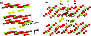 | ||
| Fig. 3 Na2V6O16·3H2O supercell structure: (a) 2 × 6 × 1 ball-type and (b) the 1 × 2 × 1 ball-and-stick type. | ||
The synthetic super-long Na2V6O16·3H2O nanobelts enable the possibility to investigate the electrical transport of single nanobelts.
In particular, owing to the existence of Na+ cations between the vanadate layers in the Na2V6O16·3H2O structure, the synthetic Na2V6O16·3H2O nanobelts are expected to have a good electronic conductivity for potential applications in nanoelectrodes and nanodevices. Then, it is essential to study the electrical transport property of the single nanobelt due to the difficulty in both the synthesis of such super-long nanobelt and the measurement of the single nanobelt. Hence, we preliminarily explore the electrical transport property of an individual single-crystalline Na2V6O16·3H2O nanobelt by scanning the bias voltage at room temperature and ambient air conditions,20 and the obtained results are shown in Fig. 4. A schematic view and the SEM image of an individual Na2V6O16·3H2O nanobelt electrode are shown in the insets of Fig. 4 top left and bottom right respectively. It is clear that the bottom-contacted device exhibits nonlinear and symmetric (I–V) characteristics for bias voltages in the range of +3 to −3 V. The curve is reproducible, and no large fluctuations are observed even in the high bias region, indicating that the device is stable. Excitingly, the electrical conductivity of synthetic individual single crystalline Na2V6O16·3H2O nanobelts exhibit a metallic nature with a conductivity of ∼100 S m−1 at room temperature, implying considerable advantage as functional electrode units mediating the transport of electrons as nanoelectrode candidates. But, the conductivity of the individual nanobelt is much larger than the electrical conductivity of the bulk Na2V6O16·3H2O,17 which may be explained by the poor orientation and greater number of grain boundaries for Na2V6O16·3H2O in the bulk state. This phenomena has also been found in the monoclinic NH4V3O8 single-crystalline nanobelts.21 Interestingly, the good conductivity of the synthetic single Na2V6O16·3H2O nanobelt suggests a new idea of designing nanomaterials with nanobelt structures to obtain good conductivity. Thus, such high quality metallic Na2V6O16·3H2O nanobelts are expected to be used as an ideal functional unit of a nanodevice.
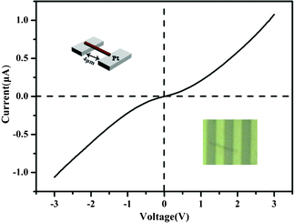 | ||
| Fig. 4 I–V curve of the Pt electrode with an individual Na2V6O16·3H2O nanobelt at 300 K. Insets: schematic view (top left) and the SEM image of the individual nanobelt electrode (bottom right). | ||
Due to the excellent electrical properties of the aligned nanobelt film electrodes, such super-long Na2V6O16·3H2O nanobelts with good electrical transport properties inspired us to align these nanobelts into film electrodes with good conductivity aiming to practical application in nanoelectrodes. Herein, we have successfully developed a facile method for the one-pot synthesis of well-aligned Na2V6O16·3H2O nanobelt films with excellent tractility and toughness for the first time. The synthesis strategy is based on the overall hydrogen bonding action throughout the whole process, starting with the growth of Na2V6O16·3H2O bundles, to their final self-assembly into Na2V6O16·3H2O capsule-like film.22Fig. 5 shows digital photographs to present the spectacular morphology for the as-synthesized Na2V6O16·3H2O samples. Fig. 5a is the original image to show that a capsule-like sample had been formed after the hydrothermal reaction was over. The length and diameter can reach up to 5 cm and 1.5 cm, respectively. Generally, wonderful tactility and toughness are identified during demonstration, where the sample retains its integrity even if it is suspended by the gravity. After washing away the removable absorbed species from the surface of the capsule, we can clearly detect that the sample possesses a smooth and shiny surface as shown in Fig. 5c. Some distinguishable textures are readily observed from the sample's body (Fig. 5a and 5b), indicating a hierarchical structure. The capsule-like sample encapsulates some solution inside, which is verified by scissoring away its side portion (Fig. 5c) and liberating the jailed solution. From the broken cross-section in Fig. 5c, some void spaces are detected, further confirming the hollow capsule-like architecture. Once the encapsulated solution is released, the original structure's collapse apparently leads to the sample's volume diminishing (Fig. 5c), implying that the sample has potential to be converted into a membrane. As demonstrated in Fig. 5d, upon spreading onto a glass slide and drying at 120 °C, the capsule-like samples are finalized to form membranes with a size up to 5 cm × 4 cm. The rugate surface of the film shown in Fig. 5d provides visual evidence to reveal the chemical composition’s transformation from the hydrated Na2V6O16·xH2O to pure Na2V6O16·3H2O as testified by X-ray diffraction measurement (Fig. 1).
 | ||
| Fig. 5 Optical pictures present the obtained film samples. (a) The image is to uncover the original state of Na2V6O16·3H2O capsule with good toughness and strength. (b) The top of the Na2V6O16·3H2O capsule. (c) After removing the absorbed species on the surface, the Na2V6O16·3H2O capsule exhibits a slick and textured morphology. By scissoring away the capsule wall, the encapsulated solution is released and the capsule wall is constrictive. (d) Na2V6O16·3H2O film with size up to 5 cm × 4 cm is finally obtained after drying it completely at 120 °C. | ||
The morphology of the synthetic aligned nanobelt film is shown in Fig. 6. Fig. 6a is the SEM image of a top view of the film and Fig. 6b is the locally magnified SEM image to present more details about the film's texture. The synthetic nanobelt thin films composed of uniform aligned super-long nanobelts with high aspect ratio are showed in Fig. 6a, 6b and 6c, respectively. Nanobelts are aligned to form a high density inter-connected film. Some interval spaces exist between the neighbouring nanobelts to generate a great number of pathways penetrating through the nanobelts. In the meantime, from Fig. 6a, we can see that the film has been densely aligned and features uniform thickness and evenly distributed nanobelts, both of which provide a solid foundation for the film's potential applications in nanoelectrodes. This method to synthesise aligned nanobelt film electrodes is proven to be easy, safe and high yielding, providing a novel strategy to obtain aligned film electrodes. Besides, to characterize the degree of alignment, nanobelt angles are manually evaluated with respect to the direction of the edge on SEM micrographs.
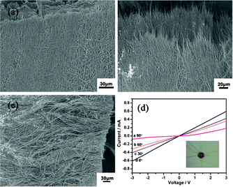 | ||
| Fig. 6 (a) SEM of the aligned synthetic Na2V6O16·3H2O nanobelt device sheet films, (b) The high magnification SEM of the aligned synthetic Na2V6O16·3H2O nanobelt device sheet films, (c) The cross-view SEM of synthetic Na2V6O16·3H2O nanobelt device sheet films, (d) The I–V curve with different angles between aligned synthetic Na2V6O16·3H2O nanobelts and the applied electrode. | ||
In order to further validate the aligned nanobelt film electrodes with the expected good conductivity, the I–V curves of aligned Na2V6O16·3H2O nanobelt film electrodes have been shown in Fig. 6d. The anisotropic current of the aligned nanobelt film electrodes can be clearly seen along with the different angles between the direction of the current flow and the direction of the aligned nanobelts. In brief, devices in which the current flows parallel to the alignment direction have been labeled as parallel devices, while devices in which current flows perpendicular to alignment direction have been labeled as perpendicular devices. As a result, the improvement in the conductivity of parallel devices is ∼10 times the conductivity of perpendicular devices (See Table 1), which confirms the anisotropic electrical transport property of the aligned nanobelt film electrodes. While current flows parallel to the alignment direction, the single crystalline super-long nanobelts provide electrical transport channels without any grain boundaries. In addition, the super-long length of the nanobelts allows the less inter-nanobelt contact resistance in the parallel devices. However, compared to the parallel devices, the shorter width or thickness of the nanobelts ensure more inter-nanobelt contact resistance and a longer path of electrical transport during similar distances of electrical transport in the perpendicular devices. In summary, the parallel devices have less inter-nanobelt contact resistance and a shorter effective path of electrical transport compared to perpendicular devices.
| 90 μm (aligned) | 85 μm (unaligned) | |
|---|---|---|
| 0° | 4850 Ω | 30![[thin space (1/6-em)]](https://www.rsc.org/images/entities/char_2009.gif) 000 Ω 000 Ω |
| 30° | 7000 Ω | 32000 Ω |
| 60° | 8500 Ω | 31000 Ω |
| 90° | 48000 Ω |
31000 Ω |
| R(0°)/R(90°) | 10 | 1.3 |
In order to further confirm the anisotropic electrical transport property of the aligned nanobelt films, a disordered nanobelt film has also been fabricated successfully and SEM images are applied to investigate the synthetic disordered nanobelt film's morphology. Fig. 7a and 7b respectively showed the top-view of the SEM images of the Na2V6O16·3H2O unaligned nanobelt electrode films, which is tangled with numerous nanobelts, and the nanobelts are cross-stacked to form an inter-connected film. Additionally, in our experiments, sometimes several layers of membranes are stacked together over the period of spreading and drying the samples, and thereby a multi-layered structure is achievable (Fig. 7c).
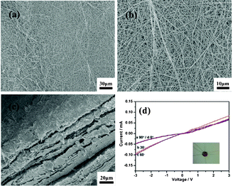 | ||
| Fig. 7 (a) SEM of the disordered synthetic Na2V6O16·3H2O nanobelt device sheet films, (b) The high magnification SEM of the disordered synthetic Na2V6O16·3H2O nanobelt device sheet films, (c) The cross-view SEM of disordered Na2V6O16·3H2O nanobelt film electrodes, (d) The I–V curve with different angles between disordered synthetic Na2V6O16·3H2O nanobelts and applied electrode. | ||
Due to the random orientation of the nanobelts in the disordered nanobelt films, the choice to the direction of current flowing parallel to the alignment direction is random. It is clear that the nearly isotropic current of unaligned nanobelt film electrodes with different directions of current flowed as shown in Fig. 7d.
Moreover, the current of the unaligned nanobelt film electrode is much smaller than the aligned nanobelt film electrode obviously. Because, compared to the aligned nanobelt films, the unaligned nanobelt film electrode has more inter-nanobelt resistance during electrical transport. Then, the electrical conductivity of the aligned nanobelt film electrode is much larger than the unaligned nanobelt film electrode, further supporting the good electrical conductivity and enhanced anisotropic electrical transport property of aligned nanobelt electrodes. As a result, designing a novel high degree aligned nanobelt film electrode would pave a new way to fabricate film electrodes with good conductivity.
In fact, the resistance of such nanobelt film electrodes would be influenced by various factors, such as nanobelt alignment distribution, nanobelt density and the direction of current flow with respect to the nanobelt distribution. Thus, the conductivity of a film would be too complex to solve analytically. Herein, a simple design of the film electrodes with different degrees of aligned nanobelts is used to better understand the good electronic conductivity of the aligned nanobelt film electrodes in this study. Therefore, the aligned nanobelt film electrodes provide a new strategy to design nanoelectrodes.
4. Conclusions
In conclusion, single crystalline super-long Na2V6O16·3H2O nanobelts with aspect ratios exceeding 1000 have been fabricated via a simple hydrothermal approach based on regulating the acidity of Na3VO4 precursor solution for the first time. Moreover, the electrical transport property of the individual super-long Na2V6O16·3H2O nanobelt is first found to be metallic conductivity. As expected, these aligned uniform metallic sodium vanadium bronze nanobelt film electrodes show enhanced anisotropic electrical transport property and high electrical conductivity, which is ascribed to the lesser amount of grain boundaries, improved connectivity between nanobelts, less inter-nanobelt contact resistance, and shorter effective path of electrical transport. Thus, aligned super-long Na2V6O16·3H2O nanobelt film electrodes with good performance is expected as a preponderant electrode candidate. This work provides a new strategy to design and synthesize aligned nanobelt film electrodes with enhanced electrical transport property and good electrical conductivity.Acknowledgements
This work was financially supported by National Basic Research Program of China (No. 2009CB939901), and National Natural Science Foundation of China (No. 10979047, 90922016 and 11079004).References
- W. R. Grove, Philosoph. Mag. J. Sci., 1842, 21, 417 Search PubMed.
- A. S. Aricò, P. Bruce, B. Scrosati, J. M. Tarascon and W. V. Schalkwijk, Nat. Mater., 2005, 4, 366 CrossRef.
- Y. Huang, X. Duan, Q. Wei and C. M. Lieber, Science, 2001, 291, 630 CrossRef CAS.
- M.H. Huang, S. Mao, H. Feick, H. Q. Yan, Y. Y. Wu, H. Kind, E. Weber, R. Russo and P. D. Yang, Science, 2001, 292, 1897 CrossRef CAS.
- J. H. Song, X. D. Wang, E. Riedo and Z. L. Wang, Nano Lett., 2005, 5, 1954 CrossRef CAS.
- H. Steinberg, Y. Lilach, A. Salant, O. Wolf, A. Faust, O. Millo and U. Banin, Nano Lett., 2009, 9, 3671 CrossRef CAS.
- S. J. Kang, C. Kocabas, T. Ozel, M. Shim, N. Pimparkar, M. A. Alam, S. V. Rotkin and J. A. Rogers, Nat. Nanotech., 2007, 2, 230 CrossRef CAS.
- D. Steiner, D. Azulay, A. Aharoni, A. Salant, U. Banin and O. Millo, Phys. Rev. B, 2009, 80, 195308 CrossRef.
- Z. Hu, M. D. Fischbein, C. Querner and M. Drndic', Nano Lett., 2006, 6, 2585 CrossRef CAS.
- C. Lao, Y. Li, C. P. Wong and Z. L. Wang, Nano Lett., 2007, 7, 1323 CrossRef CAS.
- W. Chen, Q. Xu, Y. S. Hu, L. Q. Mai and Q. Y. Zhu, J. Mater.Chem., 2002, 12, 1926 RSC.
- P. P. Prosini, Y. Y. Xia, T. Fujieda, R. Vellone, M. Shikano and T. Sakai, Electrochim. Acta, 2001, 46, 2623 CrossRef CAS.
- P. Liu, S. H. Lee, H. M. Cheong, C. E. Tracy, J. R. Pitts and R. D. Smith, J. Electrochem. Soc., 2002, 149, H76 CrossRef CAS.
- J. Muster, G. T. Kim, V. Krstic, J. G. Park, Y. W. Park, S. Roth and M. Burghard, Adv. Mater., 2000, 12, 420 CrossRef CAS.
- F. Cheng and J. Chen, J. Mater. Chem., 2011, 21, 9841 RSC.
- H. Wang, W. Wang, Y. Ren, K. Huang and S. Liu, J. Power Sources, 2012, 199, 263 CrossRef CAS.
- Y. Xue, X. D. Zhang, J. J. Zhang, J. Wu, Y. F. Sun, Y. C. Tian and Y. Xie, J. Mater.Chem., 2012, 22, 2560 RSC.
- G. T. Zhou, X. Wang and J. C. Yu, Cryst. Growth Des., 2005, 5, 969 CAS.
- J. Yu, J. C. Yu, W. Ho, L. Wu and X. Wang, J. Am. Chem. Soc., 2004, 126, 3422 CrossRef CAS.
- G. Cheng, Z. Li, S. Wang, H. Gong, K. Cheng, X. Jiang, S. Zhou, Z. Du, T. Cui and G. Zou, Appl. Phys. Lett., 2008, 93, 123103 CrossRef.
- L. Q. Mai, C. S. Lao, B. Hu, J. Zhou, Y. Y. Qi, W. Chen, E. D. Gu and Z. L. Wang, J. Phys. Chem. B, 2006, 110, 18138 CrossRef CAS.
- Y. Wang, H. J. Zhang, K. W. Siah, C. C. Wong, J. Lin and A. Borgna, J. Mater. Chem., 2011, 21, 10336 RSC.
| This journal is © The Royal Society of Chemistry 2012 |