Sunlight active antibacterial nanostructured N-doped TiO2 thin films synthesized by an ultrasonic spray pyrolysis technique
N. C.
Raut
a,
Tom
Mathews
*a,
P. K
Ajikumar
a,
R. P.
George
b,
S.
Dash
a and
A. K.
Tyagi
a
aSurface and Nanoscience Division, Materials Science Group, Indira Gandhi Centre for Atomic Research, Kalpakkam, 603102, T. N, India.. E-mail: tom@igcar.gov.in; Fax: 914427480081; Tel: 914427480500 extn 22206
bCorrosion Science and Technology Division, Indira Gandhi Centre for Atomic Research, Kalpakkam, 603102, T. N, India.
First published on 11th September 2012
Abstract
Sunlight active antibacterial N-doped anatase TiO2 nanocrystalline thin films were synthesized on Si(100), quartz and glass substrates at 300–550 °C, in a single step by ultrasonic spray pyrolysis, using hexamine as the nitrogen source and characterized using field emission scanning electron microscopy, X-ray diffraction, Raman spectrometry, secondary ion mass spectrometry, X-ray photoelectron and UV-visible spectroscopy. The antibacterial activity under UV, sunlight and normal room lighting was studied and compared. The TiO2−x−3yN2y films showed enhanced antibacterial activity under room light and sunlight compared to the pristine TiO2 films. The enhanced activity with nitrogen doping is due to the photo-generated holes on the localized N 2p states above the O 2p valence band, which are mobile enough to participate in the surface redox reaction. The microstructure of the films varied from nanodot chains to triangular platelets to cuboids with increase in synthesis temperature, confirming control of morphology and size with synthesis temperature. The secondary ion mass spectrometric studies of the films revealed a uniform distribution of titanium, oxygen and nitrogen across the thickness of the film. The N-doping concentration was ∼3.4%, as confirmed by XPS. The films had a band gap of about 3.30 eV obtained from UV-Vis studies.
A Introduction
Titanium dioxide is one of the extensively studied transition metal oxides, known for its remarkable photocatalytic and optical properties. Nano-structured TiO2 thin films find application in removal of organic pollutants from water and air,1,2 destruction of microbes,3 self cleaning windows and tiles,4 and in dye sensitized solar cells.5 Among the various phases of TiO2, anatase shows superior photocatalytic activity under UV light irradiation having wavelength less than 387 nm, because of generation of electron/hole pairs under UV light irradiation. In TiO2, the valence band potential is positive enough to generate hydroxyl radicals at the surface and the conduction band potential is negative enough to reduce molecular O2 to O2− superoxide radical. The hydroxyl radicals are powerful oxidizing agents and it can oxidize organic pollutants or inactivate microbes presenting at or near the TiO2 surface. The superoxide can react with a proton generating hydroperoxyl radical (HO2−). The O2− and HO2− species bring about the oxidation of any organic compound settling on the surface.6 It has been found that particle size is an important parameter for photocatalytic efficiency. When the size of the particles become comparable with the de Broglie wavelength of the charge carriers, which lies between 5 and 25 nm for oxide semiconductors like TiO2, the wavefunction of the charge carriers spreads over the entire particle and therefore the charge carriers do not need to diffuse any more to accomplish reactions with species present at the surface.7 This increases the quantum yield. Experimental investigations support the existence of an optimum particle size of ∼10 nm for TiO2, where photocatalytic oxidation rates of organic pollutants are maximized.8 Theoretical investigations have also concluded that particle size plays significant role in the photo-activity of TiO2. A model based on the mechanism of TiO2 photocatalysis predicts an increase of the quantum yield when particle size decreases from 1000 nm to 10 nm.9 A stochastic model predicts an increase in quantum yield as particle size increase from 3 to 21 nm, because the e−–h+ recombination rates are lower for the larger particles.10 Based on the above, a particle size/confinement of size, at least in one dimension around 12 nm seem to be more effective for photocatalytic applications.The optical absorbance of TiO2, although excellent in the UV region, drastically declines in the visible range (the visible region constitutes 45% of sunlight). This has limited the use of TiO2 in photoassisted applications, but opened a new field, that is engineering the TiO2 band gap to make it an efficient photocatalyst under sunlight or even poorly illuminated interior lighting. Early attempts in shifting TiO2 absorption into the visible light region mainly focused on doping with transition metal ions.11–13 Band gap engineering by cation doping revealed that many of the cations do not result in free charge carriers but in bound excitons. In addition, thermal instability and a tendency to form charge carrier recombination centers make it impractical. Modification by anion substitution was found to be more promising, of which, substituting oxygen by nitrogen seems to be the most effective due to its similar size to oxygen and small ionization energy.14 Because of the comparable ion size, the lattice distortion will be less and hence large numbers of recombination centers are not generated. It has been indicated from theoretical calculations that by N-doping the electronic band structures of TiO2 are modified by the N-2p–O-2p hybridization and consequent delocalization, resulting in the upward shift of the valence band.15 Density functional theory calculations indicate that substitution of oxygen by nitrogen atoms in TiO2 can create an isolated localized N 2p state above the O 2p dominant valence band.16–21 Also the mixing of N 2p with O 2p is less pronounced if N substitutes the O sites. It has been reported that the band structure modification depends on doped nitrogen concentration and band narrowing can occur when doping levels reach a critical concentration of 20% in anatase TiO2. The possible electronic structural changes that occur on doping are given in a recent review by Qiu and Burda.22 The superiority of N-doped TiO2 is demonstrated from the view point of photocatalytic activity,23–25 surface hydrophilicity,26 and photoinduced carrier response27 under visible light illumination.
N-doped TiO2 thin films are generally synthesized by sputtering,28 laser ablation,29 ion implantation,30 high temperature annealing of TiO2 films in the presence of amine precursors, such as ammonia and urea,31–33 chemical vapor deposition (CVD),34 atmospheric pressure CVD (APCVD)35 and sol–gel.36,37 Among these techniques, the sol–gel technique is low cost and easy to manipulate. In the sol–gel technique, Ti precursors are hydrolysed in alcohol and water in the presence of nitrogen precursors, such as ammonia and organic amines, and are mainly used for powder synthesis. One can also use it for the synthesis of thin films by suitably engineering the precursors. The commonly adopted sol–gel coating techniques are spin coating, dip coating and spray pyrolysis. Dip coating/spin coating need repeated dipping/spinning and heating to get the required thickness. In the case of spray pyrolysis the required coatings are obtained in a single step and are suitable for large surface area coatings. The process consists of atomization of the precursor solution and transportation of the resulting aerosols towards the hot substrate by a carrier gas. Within the hot zone above the substrate, the precursors undergo vaporization followed by reactive decomposition at the substrate surface, in the presence of oxygen, resulting in oxide film formation.38 While studies on the photocatalytic and self cleaning properties of N-doped TiO2 films are available in the literature, there are not many reports on the antimicrobial properties of N-doped TiO2 films. To our knowledge there is only one report on visible light assisted antibacterial properties of N-doped TiO2 films.35 Recently Nakano et al.39 reported photocatalytic inactivation of the influenza virus by TiO2 thin films under UV light. The paper by Dunnill et al.35 and the references therein give the various synthesis methods adopted for growing N-doped TiO2 films, their photocatalytic activities, nature of N-incorporation (substitutional , NO, or interstitial, Ni) and effect of nature of doped N (Ni and/or NO) on photocatalytic activity. Dunnill et al.35 synthesized the N-doped films by APCVD using titanium chloride, ethyl acetate and t-butylamine vapors carried by nitrogen gas at different flow rates, at 500 °C in a CVD reactor. Synthesis of N-doped TiO2 films, reported hitherto, were generally done in specified atmospheres under closed conditions. From the commercial point of view, developments of open atmospheric techniques are important as they are easy to use, cost effective and suitable for large scale production.
In the present study, we report the synthesis of nanodot chains as well as self aligned nano-platelets of N-doped TiO2, with size confinement in thin film form, by ultrasonic spray pyrolysis, a facile and very cost effective open atmospheric technique, and their antimicrobial properties. N-doping is achieved by using hexamine as the nitrogen precursor. The structural and morphological correlations were drawn from grazing incidence X-ray diffraction studies (GIXRD), Raman spectroscopy and field emission scanning electron microscopy (FESEM). X-ray photoelectron spectroscopy (XPS) was used to investigate the elemental composition of the N-doped TiO2 thin films. Compositional depth profiling was performed using secondary ion mass spectrometric (SIMS) analysis. Optical band gap was evaluated using ultraviolet-visible (UV-Vis) absorption spectroscopy. The antibacterial properties of the N-doped TiO2 films were studied at near UV (∼380 nm), normal room light (under lighting conditions commonly found in interior households and hospitals in India) and sunlight.
B Experimental
Synthesis of N-doped TiO2 thin films
The experimental set up and the parameters employed for the synthesis of nanostructured thin films are published elsewhere.40 However, for the sake of completeness, a brief account is being furnished here. The spray pyrolysis set up consists of an ultrasonic atomizer, a heater and a quartz column. The precursor solution was prepared by dissolving 0.05 M titanium oxy-acetyl acetonate and hexamine in methanol. A static ultrasonic nebulizer with 1.7 MHz resonator was employed to generate aerosols having a fairly uniform size distribution in the range 1–3 μm. The aerosols were transported to the substrates fastened on to a flat heater. The substrate temperature was varied from 300–550 °C. The quartz, Si (100) and glass substrates were cleaned chemically in acidic and basic baths, and then ultrasonicated in isopropanol before being loaded onto the substrate holder. The aerosols on reaching the hot zone evaporated and the vapors reacted with oxygen at the substrate surface to form the desired thin film.Characterization
The thickness of the films was measured using a surface profilometer (Dektak). The crystal structure of the film was characterized by GIXRD (STOE, Germany) using Cu-Kα radiation and 0.5° angle of incidence in back scattering geometry. The Raman spectroscopic studies were carried out using Micro-Raman Spectrometer (Jobin Yvon HR800) 514 nm Ar+ ion laser, equipped with a power of 0.5 mW and 100× objective lens. The surface morphology of the thin films was characterized using FESEM (Ziess Germany). XPS studies on the thin films were carried out using SPECS make photoelectron spectrometer. Depth profile analyses of the thin films were carried out by CAMECA IMS-4f SIMS machine. Cs+ ion beam with 1.75 kV impact voltage and 10 mA current with beam diameter of ∼5 μm was rastered over an area of 100 μm2 for the depth profile analysis. Optical absorption spectra of the thin films were recorded at room temperature using double beam UV-Visible spectrophotometer (Shimadzu-3101PC) in the wavelength range 190–890 nm.Anti-bacterial studies
The bacterial species Pseudomonas aeruginosa was isolated from a fresh water biofilm and identified up to genus level using biochemical tests (APHA, 1989).41 The small rod like structure of Pseudomonas aeruginosa cells as gram-negative rods were observed under an optical microscope. The isolated pathogen Pseudomonas aeruginosa were then cultured in a 10% nutrient broth to mimic the natural aquatic environment. Plain glass substrates as well as glass substrates coated with TiO2 and N-doped TiO2 thin films at 500 °C were exposed to the cultured pathogen for 24 h to allow a considerable number of viable bacteria to settle on the surface and form a biofilm. After 24 h of exposure, the specimens were withdrawn and gently washed to get rid of the loosely adhering cells and allowed to dry in air. Three sets of specimens, each set having five plain, TiO2 coated and N-doped TiO2 coated glass plates, were kept in near UV (∼380 nm) light, room light and sunlight of intensities 1.4 mW cm−2, 0.12 mW cm−2 and 10.5 mW cm−2, respectively, for 6 h. The sunlight/room light and near UV light intensities were measured using the visible (Lutron LX-101) and UV light (Lutron UV 304A) meters, respectively. After exposure, two specimens of each condition were used for direct microscopic observation using an epifluorescence microscope and the other three for total viable count (TVC) analysis. For microscopic observation, the specimens were gently washed with sterile water and air-dried in a sterile chamber. The surface was then flooded using 0.1% acridine orange (AO) in distilled water. After 2 min, the excess stain was drained off and the specimens were washed in sterile water, dried and observed under an epifluorescence microscope (Nikon Eclipse E600; excitation filter BP 490; barrier filter O 515).42 In order to obtain the number of colony forming units (CFU) by the TVC method, the bacterial cells on the specimens, after irradiation, were dispersed in 50 ml of sterile phosphate buffer (0.0425 g KH2PO4, 0.19 g MgCl2 per liter) by sonication. Serial dilutions of the bacterial cell suspensions were then prepared and 0.1 ml of each dilution was plated onto Zobell Marine Agar (ZMA) prepared from Hi Media M 384. The plates were incubated for 24–48 h at 32 °C and the number of colonies was counted and results expressed as the number of colony forming units (CFU) per cm2 of the specimen.41 Statistical analysis of the data was carried out using the MYSTAT software. Three replicates were analyzed for each experimental condition. The Student t-test was performed to assess the significance between the bacterial counts on the control and the coated surfaces. One N-doped TiO2 coated glass substrate after use was sonicated and washed well in sterile water and retested for its antibacterial activity. Since the test was carried out on another day the sunlight intensity was different from the one given above.C Results and discussion
Glancing incidence X-Ray diffraction studies
The GIXRD patterns of the films grown on Si (100) at 350–550 °C, in steps of 50 °C, are shown Fig. 1a. The thin films synthesized on all the substrates at 300 °C are amorphous and those synthesized at 350–550 °C are of anatase phase, as evidenced from the GIXRD patterns (JCPDS 21-1272, space group I41/amd). The most intense peak appears at a 2θ value of 25.30°, which corresponds to the (101) plane of anatase phase. This peak is used to calculate the crystallite size following the Scherrer formula. The crystallite size was found to be in the range 8–15 nm for the thin films grown at 350–450 °C. The crystallite size deduced for the films grown at 500 and 550 °C could not be compared with those of films grown at 350–450 °C as the film thickness reduced drastically with an increase in substrate temperature. Typical film thickness at temperatures of 350 °C and 550 °C on Si(100) are about 200 nm and 50 nm, respectively. With respect to substrate and for a given deposition condition, the thickness increases in the order Si (100) < quartz < glass. When the crystallites try to grow bigger in size with the increase in the temperature, the film is expected to experience reduced strain. This is evidenced from the decreasing trend in 2θ values with increase in synthesis temperature. The strain relaxation could have caused the morphological change, as seen from the FESEM images, as strain relaxation can give rise to shape transition.43Raman spectroscopic studies
The N-doped TiO2 thin films synthesized by spray pyrolysis are responsive to Raman scattering. Raman spectra of the N-doped TiO2 thin films synthesized on quartz at temperatures of 350–550 °C are shown in Fig. 1b. The Raman spectrum demonstrates that the grains of the nanocrystalline N-doped TiO2 thin films grown on quartz are well crystallized anatase phase. All the Raman bands characteristic to the anatase phase of TiO2 could be recorded. An intense band at 143 cm−1 (Eg(1)), a weak band at 198 cm−1 (Eg(2)) and the three medium intensity bands at 397 cm−1 (B1g(1)), 514 cm−1 (A1g + B1g(2)) and 635 cm−1 (Eg(3)) were observed. These values for Raman modes agreed well with the literature values for anatase TiO2.44,45 The intense low frequency band at 143 cm−1 is due to O–Ti–O bending vibrations and is a characteristic feature of the anatase phase.45,46 The weak vibrational mode at 790 cm−1, is due to the bending vibration of Si–O–Si groups belonging to the substrate.47 The broad peak found near 1590 cm−1, corresponds to the graphitic G band and is due to the presence of carbon, with sp2 type bonding of free non-reducible carbonaceous materials deposited on the film surface, along with N-doped TiO2.48 The broadening of the G band is due to the increase in disorder. The carbon content originated from the precursor solution (titanium oxy-acetyl acetonate) and is not bonded to TiO2. It is observed that at a temperature ≥500 °C the deposition of carbon materials is insignificant. This could be due to the high temperature surface oxidation of carbon-bearing species to gaseous products. Similar results were obtained for N-doped TiO2 thin films grown on glass and Si(100) at 350–550 °C, but with low intensities compared to that grown on quartz. | ||
| Fig. 1 GIXRD pattern of the N-doped TiO2 thin films synthesized on Si(100) at substrate temperatures of 350–550 °C. Fig. 1b. Raman spectra of the N-doped TiO2 thin films grown on quartz at temperatures of 350–550 °C. | ||
Scanning electron microscopic studies
The FESEM images of the films grown on Si(100) at substrate temperatures in the range 350–550 °C are given in Fig. 2a–2e. Fig. 2a depicts the morphology of the film grown at 350 °C. The surface appears very smooth without any well defined grains. The surface morphology of the film synthesized at 400 °C (Fig. 2b) indicates the formation of groups of linear nanodot chains, each group oriented in a different direction. The size of the nanodots is of the order 8–10 nm. The surface morphology of the films grown at 450 °C (Fig. 2c) shows nanodot chains agglomerated in a triangular form. The formation of well defined triangular nanoplatelets, of ∼10–15 nm thickness, can be discerned from the FESEM images of the sample prepared at 500 °C (Fig. 2d). The film thickness is about the height of the triangular platelets. Fig. 3e shows the morphology of films synthesized at 550 °C. The film consists of well separated cuboid grains. The film thickness is that of the cuboids. From the FESEM images, considering the de Broglie wave length of 5–25 nm for charge carriers in oxide semiconductors like TiO2, quantum confinement in the case of films grown at 350–450 °C and the possibility of confinement in one dimension for the films grown at 500 °C cannot be ruled out. The FESEM results confirm morphology and size control with synthesis temperature. The morphologies of the films grown on glass and quartz were also found to vary with temperature in a similar fashion. | ||
| Fig. 2 FESEM micrographs of N-doped TiO2 thin films grown on Si(100) at substrate temperatures of (a) 350 °C, (b) 400 °C, (c) 450 °C, (d) 500 °C, (e) 550 °C. | ||
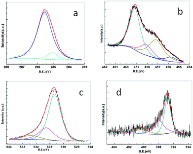 | ||
| Fig. 3 X-ray photoelectron spectra details collected from the N-doped TiO2 thin film deposited at 500 °C (a) C 1s, (b) Ti 2p3/2, (c) O 1s and (d) N 1s core levels. | ||
X-ray photoelectron spectroscopic studies
An XPS study of N doped TiO2 thin film deposited at a substrate temperature of 500 °C has been undertaken in order to understand the stoichiometry and bonding nature. Typical spectra of C 1s, Ti 2p, O 1s and N 1s are shown in Fig. 3(a), 3(b), 3(c) and 3(d), respectively. The C 1s XPS spectrum in Fig. 3(a) shows the peak position at 285.04 eV, which corresponds to amorphous carbon.49 This carbon is not bonded to Ti. The binding energies obtained for Ti 2p, O 1s and N 1s are corrected for specimen charging by referencing the observed C 1s binding energy to 284.5 eV. Titania synthesized by various techniques exhibits nonstoichiometry and it varies with synthesis technique. In the present study both pure and N-doped titania were synthesized by using metal organic precursors. Because of the presence of reducing species (C and H) in the precursor, titania synthesized under the present conditions is oxygen deficient (TiO2−x) as evidenced from XPS ananlysis.50 To maintain charge neutrality the presence of oxygen vacancies will lead to the formation of lower valent Ti ions. In the case of N-doped titania synthesized in the present study, because of the very similar synthesis conditions (except for the presence of the nitrogen-generating precursor, hexamine, in the solution), additional oxygen vacancies due to N-doping are created. One oxygen vacancy is generated for every two N-atoms incorporated into the anion lattice. Therefore, the general formula of N-doped titania can be written as TiO2−x−3yN2y. Fig. 3b shows the high resolution XPS spectra of Ti 2p3/2 core level of as prepared N-doped TiO2 films on Si(100) at 500 °C. The peak is asymmetric with a shoulder at the lower binding energy side, indicating the presence of lower valence Ti ions. In order to distinguish the Ti ions of different valances, peak fitting of X-ray photoelectron spectra were performed using XPS fit software. The electron background correction was carried out using the Shirley (nonlinear) background correction method, being the most commonly accepted and widely used one among the various background correction methods.51,52 For the background correction the energy window taken was 462–454 eV. The background corrected spectra were fitted by assuming Gaussian profiles for different chemical states. The parameters which define the XPS core level peaks are peak position or binding energy, full width at half maximum (FWHM), peak area and peak intensity. By an intricate peak fitting process the spectra have been resolved into 4 spin orbit components of binding energies 459.16, 458.1, 457.15 and 455.75 eV, which are assigned as Ti4+ (TiO2), Ti3+ (TiOOH), Ti3+ (coordinatively unsaturated i.e. Ti3+ adjacent to oxygen vacancy) and Ti3+ adjacent to nitrogen, respectively. The binding energy values obtained from the deconvoluted spectrum given in Fig. 3b agree with the reported values.53–55 | ||
| Fig. 4 SIMS profile of N-doped TiO2 thin film grown on Si(100) at 500 °C. | ||
Different types of oxygen species (lattice O, oxygen near an oxygen vacancy, O–Ti–N and OH) present are distinguished by the different O 1s binding energies. Fig. 3c shows the asymmetric O 1s spectrum deconvoluted to three components with minimum chi square by the same peak fitting process, where the window for the peak fitting process was 536–526 eV. The peak positions at 530.64 and 531.26 eV correspond to (Ti4+–O) and (Ti3+–O i.e. oxygen near an oxygen vacancy), respectively, in agreement with the reported values.56,57 The broad peak at 532.37 eV can be assigned to a combination of (O–Ti–N), (HO–Ti–N) and (Ti–OH/OH−).55,58 The formation of Ti(OH)xOy at the surface can be explained as follows. The oxygen vacancies at the surface take the form of missing oxide ions in the bridging oxygen row (bridging oxygen vacancies i.e. Ti3+–VO–Ti3+).59 The bridging oxygen vacancies form electron trap centers, ∼0.75 eV below the conduction band and act as adsorption sites for molecules like H2O. Therefore, when water molecules come in contact with film surface they are adsorbed at the bridging oxygen vacancies and dissociated into an OH group and H atom. The OH group fills the oxygen vacancy to form a Ti–OH–Ti bridge. The hydrogen atom has two options. It can form an identical Ti–OH–Ti bridge, by binding to another bridge (Ti–O–Ti), or Ti3+–OH by binding to O2− ions terminating at the surface. As anions are easily polarizable by cations they terminate at the surface, thereby reducing the surface potential and are active sites for reacting with the H atoms to form Ti3+–OH.60 Though the surface bridging oxygen vacancies are filled by OH groups, O1s peaks corresponding to oxygen near oxygen vacancies and Ti2p3/2 peaks corresponding to coordinatively unsaturated Ti3+ are still observed because of bulk defects.59 In addition, because of the presence of N in the anion sub-lattice, oxygen species corresponding to N–Ti–OH and N–Ti–O are expected. The coordinatively unsaturated Ti3+ ions have distorted coordination geometry and have a tendency to form additional coordination and therefore play an important role in the photo-oxidation of organic species.59 Therefore we can infer that the presence of bridging oxygen vacancies is a necessary condition for water dissociation or organic oxidation and photocatalytic efficiency increases with increase in oxygen vacancy. The observed enhancement in photocatalytic efficiency with N-doping can be explained due to the increase in bridging oxygen vacancies with doping.
The high resolution N-1s spectra consist essentially of three peaks viz. one high intensity peak at 396.87 eV and two low intensity peaks at 397.7 and 400.4 eV. The different N-1s BE values represent different electron density around nitrogen suggesting various N environments in the lattice. The high intensity peak at 396.8 and the low intensity peaks at 397.7 eV can be ascribed to substitutional nitrogen in the oxide lattice (NO).61 The structure of anatase TiO2 consists of corner and edge sharing (TiO6) octahedra. If the number of oxygen atoms substituted by nitrogen atoms in each octahedron is the same (nitrogen substitution uniformly distributed throughout) one would expect a single N 1s BE value corresponding to NO (N–Ti–O) species. If the number of N ions in the co-ordination sphere around Ti varies, the observed N 1s values will lie in a range leading to N 1s peak broadening and asymmetry. In such a situation the asymmetric peak on deconvolution shows different BE values. In addition, when two oxygen atoms are substituted by nitrogen atoms one oxygen vacancy is generated. This will distort the octahedra having vacancies, as neighboring anions relax towards the vacancy, adding small changes in N 1s BE values. Hence, the reason for observing a low intensity peak at 397.7 on deconvoluting, corresponding to N–Ti–O, in addition to the high intensity peak at 396.8 eV. Based on ref. 35 and the references therein the peak at 400.4 eV is assigned to interstitial nitrogen (Ni). From the low peak intensity it is clear that the amount of Ni present is very low.
The Ti, O and N contents in the films were estimated from peak area and sensitivity factor using the equations
| XTi = (ITi/STi)/[(ITi2p 3/2/STi) + (IO/SO) + (IN/SN)] |
| XO = (IO/SO)/[(ITi2p 3/2/STi) + (IO/SO)+ (IN/SN)] |
| XN = (IN/SN)/[(ITi2p 3/2/STi) + (IO/SO) + (IN/SN)] |
From the present study and the existing literature we conclude that the presence of lower valent Ti ions (oxygen vacancies) introduce surface defects in the TiO2−x−3yN2y films, resulting in the creation of 3d defect states in the conduction band leading to a high density of electrons. This situation can increase the diffusion of the molecular adsorbate, leading to increased catalytic activity.
Secondary ion mass spectrometric studies
The spatial and depth distribution of different elements in the nano-crystalline N-doped TiO2 thin film coated on Si(100), at a substrate temperature of 500 °C, obtained from SIMS analysis is given in Fig. 4. It shows the intensities of Ti, O, C and N throughout the depth of the thin film over the Si substrate. The Ti, O and C profiles are flat and uniform across the thickness of the film up to the film–substrate interface. The intensity of N across the thickness of the film, though nearly flat, a slight decrease with the increase in the depth can be discerned. The Si profile originating from the substrate shows that the TiO2 film is condensed over the substrate. It also reflects the highly dense nature of the thin film. Similar results were obtained in the case of films grown on other substrates. The depth profile reveals compositional uniformity, especially uniform N-concentration.UV-visible spectroscopic studies
The UV-Vis absorption spectra of the thin films grown at temperatures of 350, 400, 450 and 500 °C are shown in Fig. 5(a). The absorbance is higher for the thin film grown at 350 and 400 °C. The absorbance of the N-doped TiO2 thin films is higher in case of those deposited at 400 °C than for those deposited at 350 °C. This is due to the change in size and shape of the crystallites as observed in FESEM. Such shape transitions and microstructural alterations can enhance structural anisotropy, which results in distortion in energy bands that cause altered spectral absorbance characteristics. The band gap energies were calculated from the optical absorbance data. The theory of inter band optical absorption shows that at the absorption edge, the optical absorption coefficient (α) varies with the photon energy (hν) according to the expression| (αhν)n = A(hν − Eg) | (1) |
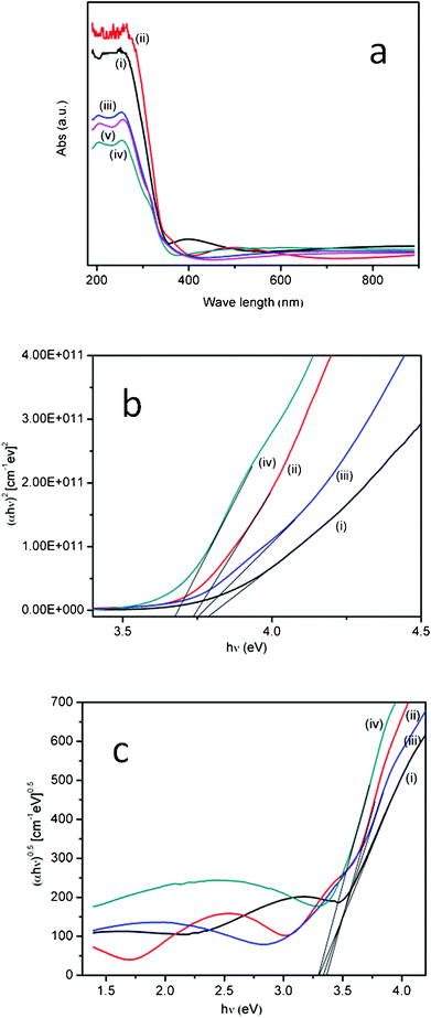 | ||
| Fig. 5 (a) UV-Vis spectra of N-doped TiO2 thin films grown on quartz from 350–550 °C; (i) 350 °C, (ii) 400 °C, (iii) 450 °C, (iv) 500 °C, (v) 550 °C. (b) Plot of photon energy (αhν)2 against (hν) of the N-doped TiO2 thin films grown on quartz; (i) 350 °C, (ii) 400 °C, (iii) 450 °C, (iv) 500 °C (c). Plot of photon energy (αhν)0.5 against (hν) of the N doped TiO2 thin films grown on quartz; (i) 350 °C, (ii) 400 °C, (iii) 450 °C, (iv) 500 °C. | ||
Antibacterial property studies
Antibacterial studies were performed using thin films synthesized at 500 °C as these films were relatively dense and of well defined morphology. Epifluorescence micrographs were taken to obtain direct evidence of antibacterial activity of the TiO2 and N-doped TiO2 coatings. The colors reflected from the micrograph indicated the state of the bacteria on the surface.66 The orange fluorescence indicates an active biofilm and the absence of fluorescence indicates dead cells. In the case of active bacteria, the AO complexed with the RNA and emitted an orange-red fluorescence on excitation. Since active cells have more RNA for protein synthesis more orange-red fluorescence is emitted. Good antibacterial activity is indicated by the absence of fluorescence and a fewer number of cells attached. It was found that the TiO2 film shows good antibacterial activity only in the UV light, whereas the N-doped TiO2 thin films showed the best antibacterial activity in sunlight, (Fig. 6). The number of CFU on the specimens before photo-irradiation, obtained from TVC studies, was in the range of ∼3 × 10⁷ to ∼108. Fig. 7 and Table 1 depict the bacterial density on surfaces obtained from the TVC study. The TVC results show reduced bacterial adhesion on the N-doped TiO2 film, indicating photocatalytic activity even in normal room light and sunlight. The used N-doped TiO2 coated glass substrates, after sonication and washing in sterile water followed by drying in air, were tested again for antibacterial activity and found to retain the same. Under sunlight of ∼8.0 mW cm−2 intensity a 4 log reduction in CFU was observed. | ||
| Fig. 6 An epifluorescence micrograph of biofilms of Pseudomonas aeruginosa on a TiO2 film (a–c) exposed to room light, near UV light and sunlight, respectively, and N doped TiO2 film (d–f) exposed to room light, near UV light and sunlight. | ||
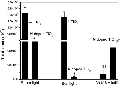 | ||
| Fig. 7 Total viable count of bacteria on TiO2 and N doped TiO2 films on glass under room light, sunlight and near UV light. | ||
| Surfaces/conditions | Room light Mean ± S.D CFU/cm2 | Sun light Mean ± S.D CFU/cm2 | Near UV light Mean ± S.D CFU/cm2 |
|---|---|---|---|
| TiO2 thin films | 2.14 × 10⁷ ± 0.45 × 10⁷ | 1.8 × 10⁷ ± 0.45 × 10⁷ | 1.11 × 10³ ± 0.84 × 10³ |
| N-doped TiO2 thin films | 3.2 × 10⁴ ± 0.11 ×10⁴ | 6 × 10² ± 0.67 × 10² | 6.7 × 10³ ± 0.77× 10³ |
In the case of pure TiO2 films, good antibacterial activity was observed only under near UV light. When a TiO2 photocatalyst absorbs a photon with energy equal to or greater than its band-gap (near UV light in the present case), an electron/hole pair is generated. The generated free electron and free hole “walk randomly” to the surface of the photocatalyst and are trapped there. The trapping of charge carriers at the surface suppresses recombination and increases the probability of interfacial charge transfer,67,68 a necessary condition for effective photocatalysis. For nanocrystalline TiO2 films, electron trap states are at about 0.5–0.7 eV below the conduction band edge69–71 and are ascribed to the presence of oxygen vacancies.72,73 Different kinds of trap sites exist for holes (deep hole traps and shallow hole traps) on the surface of TiO2 nanocrystalline photocatalysts. The shallow holes exist ∼0.5 eV above the valence band74 and react very rapidly with chemisorbed substances; the oxidation process is even competitive with the ultrafast charge trapping.75 Deeply trapped holes, however, prefer to react with more mobile physisorbed substances, due to their localized nature; the reaction is often a slower process. The electrons react with surface adsorbed oxygen molecules to form superoxide ions (O2−). The trapped electrons are reported to react more rapidly with adsorbed oxygen than free electrons.74 The holes react with adsorbed hydroxyl groups (OH−) to produce .OH radicals, which then couple to form H2O2. These intermediate species were found to play a major role in the photocatalytic destruction of organics.76–79
Photo-killing of bacteria on the illuminated TiO2 surface could be divided into three steps viz. disordering of the outer membrane of bacteria cells by reactive species (.OH, H2O2, .O2−), disordering of the inner cytoplasmic membrane and killing of the cell followed by decomposition of the dead cell80. In the first stage, the outer membranes of the pathogen are partially decomposed by the reactive species produced by the TiO2 photocatalyst. During this stage, cell viability is not lost very efficiently. The partial decomposition of the outer membrane, however, changes the permeability to reactive species. Consequently, reactive species easily reach and attack the inner membrane, leading to the peroxidation of the membrane lipid. The structural and functional disordering of the cytoplasmic membrane, due to lipid peroxidation, result in loss of cell viability and cell death. If the illumination is continued for a sufficiently long time, the dead cell decomposes completely.81
N-doping of TiO2 leads to the formation of localized N 2p states (∼0.5 eV) above the valence band and oxygen vacancies (Ti3+ 3d states) at about 0.5–0.7 eV below the conduction band edge,77 which are closer to the energy levels of shallow hole traps (∼0.5 eV) and electron traps, respectively. Irradiation with visible/sunlight promotes electrons from the N 2p states to the conduction band. The holes, formed by charge separation, remain localized on the N 2p states. Since the energy levels of shallow hole and electron traps at the surface are in the range of those of localized N 2p and Ti3+ 3d (oxygen vacancy) states, respectively, the visible light generated surface holes, at the N 2p levels, and electrons are expected to be highly reactive.75 The holes generated in the localized N 2p states are mobile enough to participate in surface redox reactions.82,83 In addition, oxygen vacancies also contribute to the absorption in the visible light region.77 These result in good photo catalytic cell destruction, by N-doped TiO2 under visible light, as observed in the present study.
It has been observed in the present study that near UV light activity of pristine and N-doped TiO2 films are comparable (Table 1). The comparable visible/room and near UV light activity of N-doped TiO2 can be ascribed to the enhanced visible light absorption and suppression of recombinative losses introduced by oxygen vacancies.84,85 The antibacterial activity of N-doped TiO2 under near UV light was found to be lower than that under sunlight, though the reverse is expected. This is because of the difference in radiation intensities. The intensity of sunlight was 10.5 mW cm−2 whereas that of near UV light used was only 1.4 mW cm−2.
As given in ref. 35 and the references therein, there is much contention and confusion about the effect of the nature of N-doping (Ni or NO) on the photocatalytic activity of N-doped TiO2. The various arguments in favor of Ni and/NO are given in the review by Thompson and Yates.86 The results of Dunnill et al.35 point to enhancement in photocatalytic activity due to Ni, whereas the results obtained in the present study indicate enhancement in photocatalytic activity due to NO. However, the presence of a very small amount of Ni observed in the present study cannot be ignored. Further studies are required to delineate the discrepancy. The antimicrobial activities obtained in the present study are comparable to those obtained by Dunnill et al.,35 though our irradiation time (6 h) is less than theirs (24 h).
D Conclusion
N-doped TiO2 thin films were grown on Si(100), quartz and glass substrates, by open atmospheric ultrasonic spray pyrolysis technique in a single step without any post annealing/chemical treatment, at various temperatures ranging from 300–550 °C in 50 °C steps. The films synthesized on all the substrates at 300 °C were amorphous. The films deposited at high temperature were of anatase phase, as confirmed from GIXRD and Raman studies. The Raman spectra showed the presence of a graphitic G band at 1590 cm−1 in films grown on quartz and glass substrates at low deposition temperatures, which corresponds to the free residual carbon in the films. FESEM studies showed that the morphology of the N-doped TiO2 films changed from nano-dot chains to nano platelets and then to cuboids with an increase in the substrate temperature. The XPS spectra of the thin films revealed N-incorporation into the anion sub-lattice as well as the presence of lower valent Ti ions and oxygen vacancies. The O![[thin space (1/6-em)]](https://www.rsc.org/images/entities/char_2009.gif) :Ti ratio in excess of stoichiometric TiO2, obtained from XPS results, is explained on the basis of the presence of Ti(OH)xOy on the surface. SIMS studies revealed compositional uniformity across the film thickness. N-doped TiO2 thin films were found to show enhanced antibacterial activity in sunlight as well as room light. It should be noted that, in view of adaptability for large scale production and large surface area coating, the spray pyrolysis technique is simple, cost effective and efficient compared to the techniques used for the fabrication of N-doped TiO2 thin films.
:Ti ratio in excess of stoichiometric TiO2, obtained from XPS results, is explained on the basis of the presence of Ti(OH)xOy on the surface. SIMS studies revealed compositional uniformity across the film thickness. N-doped TiO2 thin films were found to show enhanced antibacterial activity in sunlight as well as room light. It should be noted that, in view of adaptability for large scale production and large surface area coating, the spray pyrolysis technique is simple, cost effective and efficient compared to the techniques used for the fabrication of N-doped TiO2 thin films.
Acknowledgements
The authors are thankful to S. Kalavathi for GIXRD studies, Dr T. R. Ravindran for Raman analysis and Ms. M. Premila for UV-Vis studies. The authors thank Dr C. S. Sunder for constant support and encouragement.References
- G. H. Li and K. A. Gray, Chem. Phys., 2007, 339, 173 CrossRef CAS.
- Y. Chen and D. D. Dionysion, Appl. Catal., A, 2007, 317, 129 CrossRef CAS.
- J. Gopal, R. P. George, P. Muraleedharan and H. S. Khatak, Biofouling, 2004, 20, 167 CrossRef CAS.
- T. Yuranova, R. Mosteo, J. Bandara, D. Laub and J. Kiwi, J. Mol. Catal. A: Chem., 2006, 244, 160 CrossRef CAS.
- K. Fujihara, A. Kumar, R. Jose, S. Ramakrishna and S. Uchida, Nanotechnology, 2007, 18, 365709 CrossRef.
- M. R. Hoffmann, S. T. Martin, W. Choi and D. W. Bahnemann, Chem. Rev., 1995, 95, 69 CrossRef CAS.
- O. P. Carp, C. C. Huisman and A. Reller, Prog. Solid State Chem., 2004, 32, 33 CrossRef CAS.
- Z. Zhang, C. C. Wang, R. Zakaria and J. Y. Ying, J. Phys. Chem. B, 1998, 102, 10871 CrossRef CAS.
- H. Gerischer, Electrochim. Acta, 1995, 40, 1277 CrossRef CAS.
- M. A. Grela and A. J. Colussi, J. Phys. Chem., 1996, 100, 18214 CrossRef CAS.
- W. Choi, A. Termin and M. R. Hoffman, J. Phys. Chem., 1994, 98, 3669 CrossRef.
- M. I. Litter and J. A. Navio, J. Photochem. Photobiol., A, 1996, 98, 171 CrossRef CAS.
- D. Morris, R. Dixon, F. H. Jones, Y. Dou, R. G. Egdell, S. W. Downes and G. Beamson, Phys. Rev. B: Condens. Matter, 1997, 55, 16083 CrossRef CAS.
- C. H. Park, S. B. Zhang and S. H. Wei, Phys. Rev. B: Condens. Matter Mater. Phys., 2002, 66, 73202 CrossRef.
- R. Asahi, T. Morikawa, T. Ohwaki, K. Aoki and Y. Taga, Science, 2001, 293, 269 CrossRef CAS.
- C. D. Valentin, G. Pacchioni, A. Selloni, S. Livraghi and E. Giamello, J. Phys. Chem. B, 2005, 109, 11414 CrossRef.
- J. Lee, J. Park and J. Cho, Appl. Phys. Lett., 2005, 87, 11904 CrossRef.
- E. Finnazi, C. D. Valentin, A. Selloni and G. Pacchioni, J. Phys. Chem. C, 2007, 111, 9275 Search PubMed.
- H. Wang and J. P. Lewis, J. Phys.: Condens. Matter, 2006, 18, 421 CrossRef CAS.
- C. D. Valentin, G. Pacchioni and A. Selloni, Phys. Rev. B: Condens. Matter Mater. Phys., 2004, 70, 085116 CrossRef.
- K. Yang, Y. Dai, B. Huang and S. Han, J. Phys. Chem. B, 2006, 110, 24011 CrossRef CAS.
- X. Qiu and C. Burda, Chem. Phys., 2007, 339, 1 CrossRef CAS.
- Y. Irokawa, T. Morikawa, K. Aoki, S. Kosaka, T. Ohwaki and Y. Taga, Phys. Chem. Chem. Phys., 2006, 8, 1116 RSC.
- S. Yin, Y. Aita, M. Komatsu and T. Sato, J. Eur. Ceram. Soc., 2006, 26, 2735 CrossRef CAS.
- M. Liu, Q. Fang, G. He, L. Li, L. Q. Zhu, G. H. Li and L. D. Zhang, Appl. Phys. Lett, 2006, 88, 19 Search PubMed.
- J. Premkumar, Chem. Mater., 2004, 16, 3980 CrossRef CAS.
- T. Lopez-Luke, A. Wolcott, P. L. Xu, S.W. Chen, Z. H. Wen, J.H. Li, E. De La Rosa and Z. J. Zhang, J. Phys. Chem. A, 2008, 112, 1282 CrossRef CAS.
- T. Lindgren, J. M. Mwabora, E. D. A. Soto, J. Jonsson, A. Hoel, C. G. Granqvist and S. E. Lindquist, J. Phys. Chem. B, 2003, 107, 5709 CrossRef CAS.
- G. Sauthier, F. J. Ferrer, A. Figueras and E. Gyorgy, Thin Solid Films, 2010, 519, 1464 CrossRef CAS.
- O. Diwald, T. L. Thompson, E. G. Goralski, S. D. Walck and J. T. Yates, J. Phys. Chem. B, 2004, 108, 52 CrossRef CAS.
- T. Tachikawa, Y. Takai, S. Tojo, M. Fujitsuka, H. Irie, K. Hashimoto and T. Majima, J. Phys. Chem. B, 2006, 110, 13158 CrossRef CAS.
- S. Joung, T. Amemiya, M. Murabayashi and K. Itoh, Chem.–Eur. J., 2006, 12, 5526 CrossRef CAS.
- Y. Nosaka, M. Matsushita, J. Nishino and A. Y. Nosaka, Sci. Technol. Adv. Mater., 2005, 6, 143 CrossRef CAS.
- H. M. Yates, M. G. Nolan, D. W. Sheel and M. E. Pemble, J. Photochem. Photobiol., A, 2006, 179, 213 CrossRef CAS.
- C. W. H. Dunnill, Z. A. Aiken, J. Pratten, M. Wilson and D. J. Morgan, J. Photochem. Photobiol., A, 2009, 207, 244 CrossRef CAS.
- M. Drygas, C. Czosnek, R. T. Paine and J. F. Janik, Chem. Mater., 2006, 18, 3122 CrossRef CAS.
- T. Matsumoto, N. Iyi, Y. Kaneko, K. Kitamura, S. Ishihara, Y. Takasu and Y. Murakami, Catal. Today, 2007, 120, 226 CrossRef CAS.
- R. W. Schwartz, T. Schneller and R. Waser, C. R. Chim., 2004, 7, 433 CrossRef CAS.
- R. Nakano, H. Ishiguro, Y. Yao, J. Kajioka, A. Fujishima, K. Sunada, M. Minoshima, K. Hashimoto and Y. Kubota, Photochem. Photobiol. Sci., 2012, 11, 1293 CAS.
- N. C. Raut, T. Mathews, S. Tripura Sundari, T. N. Sairam, S. Dash and A. K. Tyagi, J. Nanosci. Nanotechnol., 2009, 9, 5298 CrossRef CAS.
- APHA standard methods for the examination of water and waste water, APHA, USA, 14th edn, 1989 Search PubMed.
- T. C. Mah and G. A. O Toole, Mechanism of bio-film resistance to antimicrobial agents, Trends Microbiol., 2001, 9, 34 CrossRef CAS.
- J. Tersoff and R. M. Tromp, Phys. Rev. Lett., 1993, 70, 2782 CrossRef CAS.
- M. Nicol and M. Y. Fong, J. Chem. Phys., 1971, 54, 3167 CrossRef CAS.
- T. Ohsaka, F. Izumi and Y. Fujiki, J. Raman Spectrosc., 1978, 7, 321 CrossRef.
- H. Tang, K. Prasad, R. Sanjines, P. E. Schmid and F. Levy, J. Appl. Phys., 1994, 75, 2042 CrossRef CAS.
- P. González, J. Serra, S. Liste, S. Chiussi, B. León and M. Pérez-Amor, J. Non-Cryst. Solids, 2003, 320, 92 CrossRef.
- A. C. Ferrari and J. Robertson, Phys. Rev. B: Condens. Matter, 2001, 64, 075414 CrossRef.
- J. F. Moulder, W. F. stickle, P. E. Sobol, K. D. Bomben, Hand book of photoelectron spectroscopy, ULVAL-PHI, Inc., 1995 Search PubMed.
- N. C. Raut, T. Mathews, P. Chandramohan, M. P. Srinivasan, S. Dash and A. K. Tyagi, Mater. Res. Bull., 2011, 46, 2057 CrossRef CAS.
- D. A. Shirley, Phys. Rev. B: Solid State, 1972, 5, 4709 CrossRef.
- S. Tougaard, J. Electron Spectrosc. Relat. Phenom., 1990, 52, 243 CrossRef CAS.
- H. Liu, W. Yang, Y. Ma, Y. Cao, J. Yao, J. Zhang and T. Hu, Langmuir, 2003, 19, 3001 CrossRef CAS.
- V. K. Mahajan, M. Misra, K. S. Raja and S. K. Mohapatra, J. Phys. D: Appl. Phys., 2008, 41, 125307 CrossRef.
- N. C. Saha and H. G. Tompkins, J. Appl. Phys., 1992, 72, 3072 CrossRef CAS.
- L.V. Traveira, J. M. Macak, H. Tsuchia, L. F. P. Dick and P. Schmuki, J. Electrochem. Soc., 2005, 152, B405 CrossRef.
- P. M. Kumar, S. Badrinarayanan and M. Sastry, Thin Solid Films, 2000, 358, 122 CrossRef CAS.
- J. Yang, H. Bai, Q. Jiang and J. Lian, Thin Solid Films, 2008, 516, 1736 CrossRef CAS.
- G. Ketteler, S. Yamamoto, H. Bluhm, K. Andersson, D. E. Starr, D. F. Ogletree, H. Ogasawara, A. Nilson and M. Salmeron, J. Phys. Chem. C, 2007, 111, 8278 CAS.
- L. Gang, L. Feng, W. Dai Ming, L. Chang, M. Xiuliang, L. Q. Gao and C. Hui Ming, Nanotechnology, 2008, 19, 025606 CrossRef.
- M. Batzill, E. H. Morales and U. Diebold, Phys. Rev. Lett., 2006, 96, 261031 CrossRef.
- T. Toyoda and I. Tsuboya, Rev. Sci. Instrum., 2003, 74, 782 CrossRef CAS.
- G. G. Valle, P. Hammer, S. H. Pulcinelli and C. V. Santilli, J. Eur. Ceram. Soc., 2004, 24, 1009 CrossRef CAS.
- A. E. J Ganzalez and S. G Santiago, Semicond. Sci. Technol., 2007, 22, 709 CrossRef.
- N. C. Raut, T. Mathews, P. Chandramohan, M. P. Srinivasan, S. Dash and A. K. Tyagi, Mater. Res. Bull., 2011, 46, 2057 CrossRef CAS.
- N. Kanavillil, R. K. Sreekumari and Y. Kikuchi, Biofouling, 2002, 18, 129 CrossRef.
- M. R. Hoffmann, S. T. Martin, W. Choi and D. W. Bahnemann, Chem. Rev., 1995, 95, 69 CrossRef CAS.
- A. L. Linsebigler, G. Lu and J. J. T. Yates, Chem. Rev., 1995, 95, 735 CrossRef CAS.
- G. Redmond, D. Fitzmaurice and M. Grätzel, J. Phys. Chem., 1993, 97, 6951 CrossRef CAS.
- G. Boschloo and D. Fitzmaurice, J. Phys. Chem. B, 1999, 103, 2228 CrossRef CAS.
- G. K. Boschloo and A. Goossens, J. Phys. Chem., 1996, 100, 19489 CrossRef CAS.
- N. Serpone, D. Lawless and R. Khairutdinov, J. Phys. Chem., 1995, 99, 16646 CrossRef CAS.
- N. D. Abazovic, M. I. Comor, M .D. Dramicanin, D. J. Jovanovic, S. P. Ahrenkiel and J. M. Nedeljkovic, J. Phys. Chem. B, 2006, 110, 25366 CrossRef CAS.
- T. Yoshihara, R. Katoh, A. Furube, Y. Tamaki, M. Murai, K. Hara, S. Murata, H. Arakawa and M. Tachiya, J. Phys. Chem. B, 2004, 108, 3817 CrossRef CAS.
- Y. Tamaki, A. Furube, M. Murai, K. Hara, R. Katoh and M. Tachiya, J. Am. Chem. Soc., 2006, 128, 416 CrossRef CAS.
- A. Nambu, J. Graciani, J. A. Rodriguez, Q. Wu, E. Fujita and J. F. Sanz, J. Chem. Phys., 2006, 125, 094706 CrossRef CAS.
- Z. Lin, A. Orlov, R. M. Lambert and M. C. Payne, J. Phys. Chem. B, 2005, 109, 20948 CrossRef CAS.
- M. Mrowetz, W. Balcerski, A. J. Colussi and M. R. Hoffmann, J. Phys. Chem. B, 2004, 108, 17269 CrossRef CAS.
- C. Di Valentin, G. Pacchioni and A. Selloni, Phys. Rev. B: Condens. Matter Mater. Phys., 2004, 70, 085116–4 CrossRef.
- K. Sunada, Y. Kikuchi, K. Hashimoto and A. Fujishima, Environ. Sci. Technol., 1998, 32, 726 CrossRef CAS.
- K. Sunada, T. Watanabe and K. Hashimoto, J. Photochem. Photobiol., A, 2003, 156, 227 CrossRef CAS.
- T. Ohsawa, I. Lyubinetsky, Y. Du, M. A. Henderson, V. Shutthanandan and S. A. Chambers, Phys. Rev. B: Condens. Matter Mater. Phys., 2009, 79, 085401 CrossRef.
- J. Wang, D. N. Tafen, J. P. Lewis, Z. Hong, A. Manivannan, M. Zhi, M. Li and N. Wu, J. Am. Chem. Soc., 2009, 131, 12290 CrossRef CAS.
- A. V. Emeline, X. Zhang, M. Jin, T. Murakami and A. Fujishima, J. Phys. Chem. B, 2006, 110, 7409 CrossRef CAS.
- A. Fujishima, X. Zhang and D. A. Tryk, Surf. Sci. Rep., 2008, 63, 515 CrossRef CAS.
- T. I. Thompson and J. T. Yates, Chem. Rev., 2006, 106, 4428 CrossRef CAS.
| This journal is © The Royal Society of Chemistry 2012 |